As of December 23, 2025, Intel (NASDAQ:INTC) has officially crossed the finish line of its ambitious "five nodes in four years" (5N4Y) roadmap, signaling a historic technical resurgence for the American semiconductor giant. The transition of the Intel 18A process node into High-Volume Manufacturing (HVM) marks the culmination of a multi-year effort to regain transistor density and power-efficiency leadership. With the first consumer laptops powered by "Panther Lake" processors hitting shelves this month, Intel has demonstrated that its engineering engine is once again firing on all cylinders, providing a much-needed victory for the company’s newly independent foundry subsidiary.
However, this technical triumph comes at the cost of a significant geopolitical retreat. While Intel’s Oregon and Arizona facilities are humming with the latest extreme ultraviolet (EUV) lithography tools, the company’s grand vision for a European "Silicon Junction" has been fundamentally reshaped. Following a leadership transition in early 2025 and a period of intense financial restructuring, Intel has indefinitely suspended its mega-fab project in Magdeburg, Germany. This pivot reflects a new era of "ruthless prioritization" under the current executive team, focusing capital on U.S.-based manufacturing while European governments reallocate billions in chip subsidies toward more diversified, localized projects.
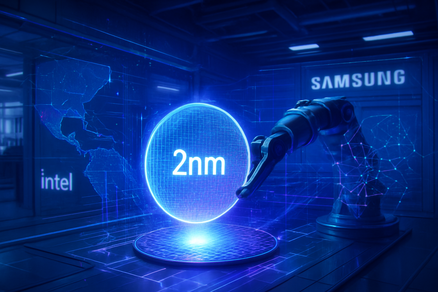
The Technical Pinnacle: 18A and the End of the 5N4Y Era
The arrival of Intel 18A represents more than just a nomenclature shift; it is the first time in over a decade that Intel has introduced two foundational transistor innovations in a single node. The 18A process utilizes RibbonFET, Intel’s proprietary implementation of Gate-All-Around (GAA) architecture, which replaces the aging FinFET design. By wrapping the gate around all sides of the channel, RibbonFET provides superior electrostatic control, allowing for higher performance at lower voltages. This is paired with PowerVia, a groundbreaking backside power delivery system that separates signal routing from power delivery. By moving power lines to the back of the wafer, Intel has effectively eliminated the "congestion" that typically plagues advanced chips, resulting in a 6% to 10% improvement in logic density and significantly reduced voltage droop.
Industry experts and the AI research community have closely monitored the 18A rollout, particularly its performance in the "Clearwater Forest" Xeon server chips. Early benchmarks suggest that 18A is competitive with, and in some specific power-envelope metrics superior to, the N2 node from TSMC (NYSE:TSM). The successful completion of the 5N4Y strategy—moving from Intel 7 to 4, 3, 20A, and finally 18A—has restored a level of predictability to Intel’s roadmap that was missing for years. While the 20A node was ultimately used as an internal "learning node" and bypassed for most commercial products, the lessons learned there were directly funneled into making 18A a robust, high-yield platform for external customers.
A Foundry Reborn: Securing the Hyperscale Giants
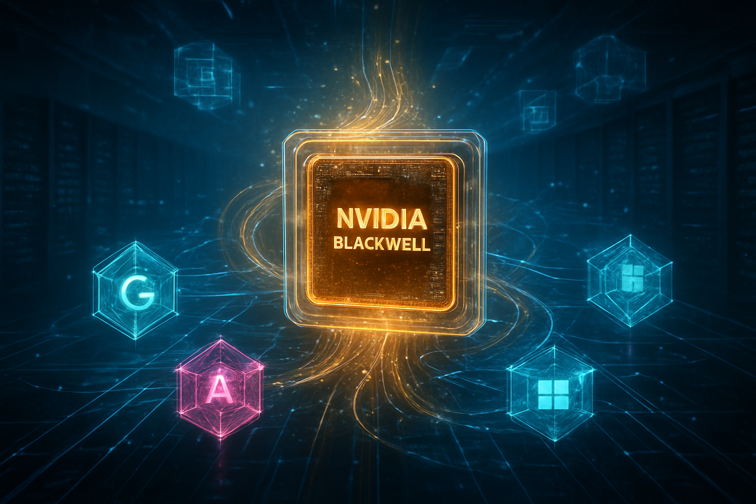
The technical success of 18A has served as a magnet for major tech players looking to diversify their supply chains away from a total reliance on Taiwan. Microsoft (NASDAQ:MSFT) has emerged as an anchor customer, utilizing Intel 18A for its Maia 2 AI accelerators. This partnership is a significant blow to competitors, as it validates Intel’s ability to handle the complex, high-performance requirements of generative AI workloads. Similarly, Amazon (NASDAQ:AMZN) via its AWS division has deepened its commitment, co-developing a custom AI fabric chip on 18A and utilizing Intel 3 for its custom Xeon 6 instances. These multi-billion-dollar agreements have provided the financial backbone for Intel Foundry to operate as a standalone business entity.
The strategic advantage for these tech giants lies in geographical resilience and custom silicon optimization. By leveraging Intel’s domestic U.S. capacity, companies like Microsoft and Amazon are mitigating geopolitical risks associated with the Taiwan Strait. Furthermore, the decoupling of Intel Foundry from the product side of the business has eased concerns regarding intellectual property theft, allowing Intel to compete directly with TSMC and Samsung for the world’s most lucrative chip contracts. This shift positions Intel not just as a chipmaker, but as a critical infrastructure provider for the AI era, offering "systems foundry" capabilities that include advanced packaging like EMIB and Foveros.
The European Pivot: Reallocating the Chips Act Bounty
While the U.S. expansion remains on track, the European landscape has changed dramatically over the last twelve months. The suspension of the €30 billion Magdeburg project in Germany was a sobering moment for the EU’s "digital sovereignty" ambitions. Citing the need to stabilize its balance sheet and focus on the immediate success of 18A in the U.S., Intel halted construction in mid-2025. This led to a significant reallocation of the €10 billion in subsidies originally promised by the German government. Rather than allowing the funds to return to the general budget, German officials have pivoted toward a more "distributed" investment strategy under the EU Chips Act.
In December 2025, the European Commission approved a significant shift in funding, with over €600 million being redirected to GlobalFoundries (NASDAQ:GFS) in Dresden and X-FAB in Erfurt. This move signals a transition from "mega-project" chasing to supporting a broader ecosystem of specialized semiconductor manufacturing. While this is a setback for Intel’s global footprint, it reflects a pragmatic realization: the cost of building leading-edge fabs in Europe is prohibitively high without perfect execution. Intel’s "European Pivot" is now focused on its existing Ireland facility, which continues to produce Intel 4 and Intel 3 chips, while the massive German and Polish sites remain on the drawing board as "future options" rather than immediate priorities.
The Road to 14A and High-NA EUV
Looking ahead to 2026 and beyond, Intel is already preparing for its next leap: the Intel 14A node. This will be the first process to fully utilize High-Numerical Aperture (High-NA) EUV lithography, using the Twinscan EXE:5000 machines from ASML (NASDAQ:ASML). The 14A node is expected to provide another 15% performance-per-watt improvement over 18A, further solidifying Intel’s claim to the "Angstrom Era" of computing. The challenge for Intel will be maintaining the blistering pace of innovation established during the 5N4Y era while managing the immense capital expenditures required for High-NA tools, which cost upwards of $350 million per unit.
Analysts predict that the next two years will be defined by "yield wars." While Intel has proven it can manufacture 18A at scale, the profitability of the Foundry division depends on achieving yields that match TSMC’s legendary efficiency. Furthermore, as AI models grow in complexity, the integration of 18A silicon with advanced 3D packaging will become the primary bottleneck. Intel’s ability to provide a "one-stop shop" for both wafer fabrication and advanced assembly will be the ultimate test of its new business model.
A New Intel for a New Era
The Intel of late 2025 is a leaner, more focused organization than the one that began the decade. By successfully delivering on the 18A node, the company has silenced critics who doubted its ability to innovate at the leading edge. The "five nodes in four years" strategy will likely be remembered as one of the most successful "hail mary" plays in corporate history, allowing Intel to leapfrog several generations of technical debt. However, the suspension of the German mega-fabs serves as a reminder of the immense financial and geopolitical pressures that define the modern semiconductor industry.
As we move into 2026, the industry will be watching two key metrics: the ramp-up of 18A volumes for external customers and the progress of the 14A pilot lines. Intel has reclaimed its seat at the high table of semiconductor manufacturing, but the competition is fiercer than ever. With a new leadership team emphasizing execution over expansion, Intel is betting that being the "foundry for the world" starts with being the undisputed leader in the lab and on the factory floor.
This content is intended for informational purposes only and represents analysis of current AI developments.
TokenRing AI delivers enterprise-grade solutions for multi-agent AI workflow orchestration, AI-powered development tools, and seamless remote collaboration platforms.
For more information, visit https://www.tokenring.ai/.