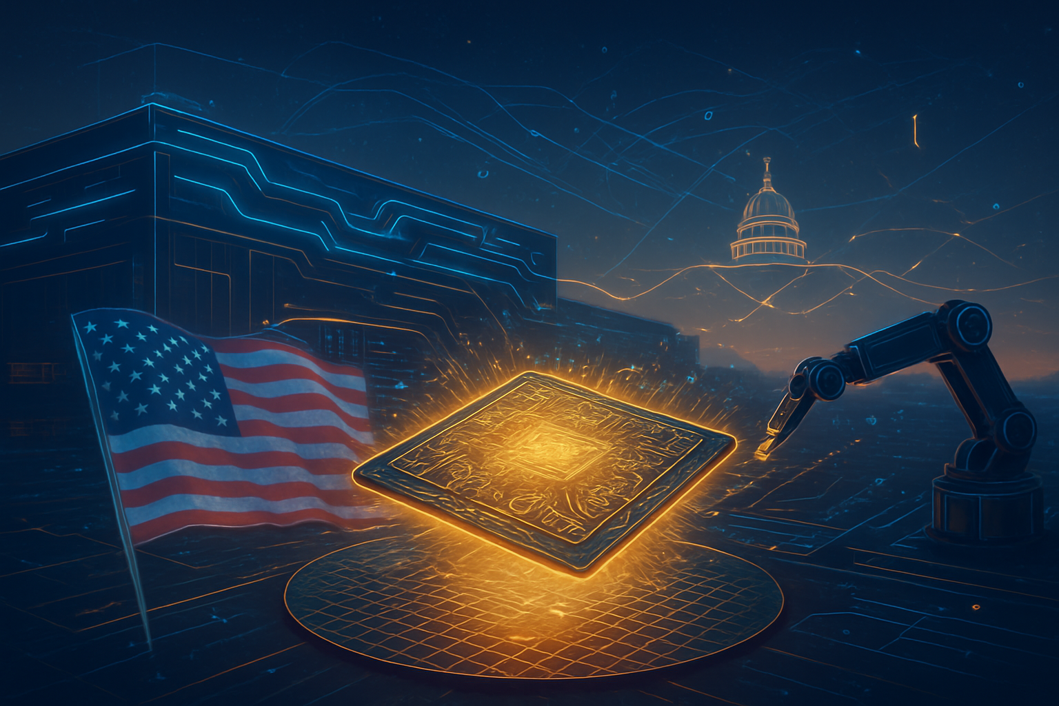
In December 2024, the Biden Administration launched what has since become the most aggressive offensive in the ongoing "chip war," a sweeping export control package that fundamentally reshaped the global artificial intelligence landscape. By blacklisting 140 Chinese entities and imposing unprecedented restrictions on High Bandwidth Memory (HBM) and advanced lithography software, the U.S. moved beyond merely slowing China’s progress to actively dismantling its ability to scale frontier AI models. One year later, as we close out 2025, the ripples of this "December Surge" have created a bifurcated tech world, where the "compute gap" between East and West has widened into a chasm.
The significance of the 2024 package lay in its precision and its breadth. It didn't just target hardware; it targeted the entire ecosystem—the memory that feeds AI, the software that designs the chips, and the financial pipelines that fund the factories. For the U.S., the goal was clear: prevent China from achieving the "holy grail" of 5nm logic and advanced HBM3e memory, which are essential for the next generation of generative AI. For the global semiconductor industry, it marked the end of the "neutral" supply chain, forcing giants like NVIDIA (NASDAQ: NVDA) and SK Hynix (KRX: 000660) to choose sides in a high-stakes geopolitical game.
The Technical Blockade: HBM and the Software Key Lockdown
At the heart of the December 2024 rules was a new technical threshold for High Bandwidth Memory (HBM), the specialized RAM that allows AI accelerators to process massive datasets. The Bureau of Industry and Security (BIS) established a "memory bandwidth density" limit of 2 gigabytes per second per square millimeter (2 GB/s/mm²). This specific metric was a masterstroke of regulatory engineering; it effectively banned the export of HBM2, HBM3, and HBM3e—the very components that power the NVIDIA H100 and Blackwell architectures. By cutting off HBM, the U.S. didn't just slow down Chinese chips; it created a "memory wall" that makes training large language models (LLMs) exponentially more difficult and less efficient.
Beyond memory, the package took a sledgehammer to China’s "design-to-fab" pipeline by targeting three critical software categories: Electronic Computer-Aided Design (ECAD), Technology Computer-Aided Design (TCAD), and Computational Lithography. These tools are the invisible architects of the semiconductor world. Without the latest ECAD updates from Western leaders, Chinese designers are unable to layout complex 3D chiplet architectures. Furthermore, the U.S. introduced a novel "software key" restriction, stipulating that the act of providing a digital activation key for existing software now constitutes a controlled export. This effectively "bricked" advanced design suites already inside China the moment their licenses required renewal.
The 140-entity addition to the U.S. Entity List was equally surgical. It didn't just target the usual suspects like Huawei; it went after the "hidden" champions of China's supply chain. This included Naura Technology Group (SHE: 002371), China’s largest toolmaker, and Piotech (SHA: 688072), a leader in thin-film deposition. By targeting these companies, the U.S. aimed to starve Chinese fabs of the domestic tools they would need to replace barred equipment from Applied Materials (NASDAQ: AMAT) or Lam Research (NASDAQ: LRCX). The inclusion of investment firms like Wise Road Capital also signaled a shift toward "geofinancial" warfare, blocking the capital flows used to acquire foreign IP.
Market Fallout: Winners, Losers, and the "Pay-to-Play" Shift
The immediate impact on the market was a period of intense volatility for the "Big Three" memory makers. SK Hynix (KRX: 000660) emerged as the dominant victor, leveraging its early lead in HBM3e to capture over 55% of the global market by late 2025. Having moved its most sensitive packaging operations out of China and into new facilities in Indiana and South Korea, SK Hynix became the primary partner for the U.S. AI boom. Conversely, Samsung Electronics (KRX: 005930) faced a grueling year; the revocation of its "Validated End User" (VEU) status for its Xi’an NAND plant in mid-2025 forced the company to pivot toward a maintenance-only strategy in China, leading to multi-billion dollar write-downs.
For the logic players, the 2024 controls forced a radical strategic pivot. Micron Technology (NASDAQ: MU) effectively completed its exit from the Chinese server market this year, choosing to double down on the U.S. domestic supply chain backed by billions in CHIPS Act grants. Meanwhile, NVIDIA (NASDAQ: NVDA) spent much of 2025 navigating the narrow corridors of "License Exception HBM." In a surprising turn of events in late 2025, the U.S. government reportedly began piloting a "geoeconomic monetization" model, allowing NVIDIA to export limited quantities of H200-class hardware to vetted Chinese entities in exchange for a significant revenue-sharing agreement with the U.S. Treasury—a move that underscores how tech supremacy is now being used as a direct tool of national revenue and control.
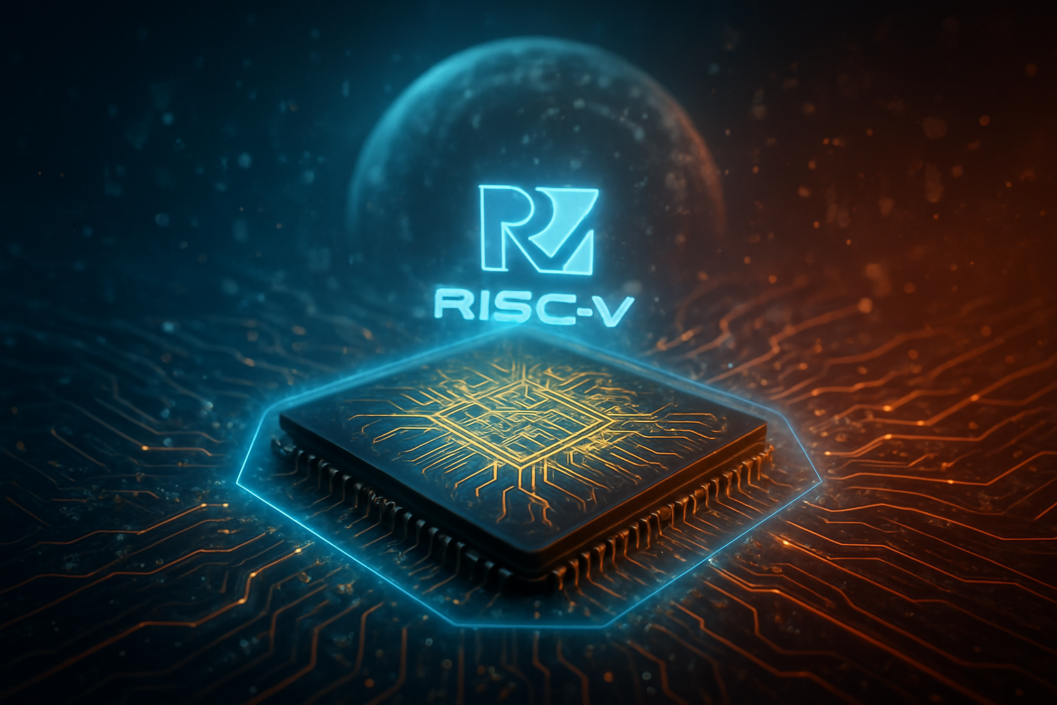
In China, the response was one of "brute-force" resilience. SMIC (HKG: 0981) and Huawei shocked the world in late 2025 by confirming the production of the Kirin 9030 SoC on a 5nm-class "N+3" node. However, this was achieved using quadruple-patterning on older Deep Ultraviolet (DUV) machines—a process that experts estimate has yields as low as 30% and costs 50% more than TSMC’s (NYSE: TSM) 5nm process. While China has proven it can technically manufacture 5nm chips, the 2024 controls have ensured that it cannot do so at a scale or cost that is commercially viable for global competition, effectively trapping their AI industry in a subsidized "high-cost bubble."
The Wider Significance: A Small Yard with a Very High Fence
The December 2024 package represented the full realization of National Security Advisor Jake Sullivan’s "small yard, high fence" strategy. By late 2025, it is clear that the "fence" is not just about keeping technology out of China, but about forcing the rest of the world to align with U.S. standards. The rules successfully pressured allies in Japan and the Netherlands to align their own export controls on lithography, creating a unified Western front that has made it nearly impossible for China to acquire the sub-14nm equipment necessary for sustainable advanced manufacturing.
This development has had a profound impact on the broader AI landscape. We are now seeing the emergence of two distinct AI "stacks." In the West, the stack is built on NVIDIA's CUDA, HBM3e, and TSMC's 3nm nodes. In China, the stack is increasingly centered on Huawei’s Ascend 910C and the CANN software ecosystem. While the U.S. stack leads in raw performance, the Chinese stack is becoming a "captive market" masterclass, forcing domestic giants like Baidu (NASDAQ: BIDU) and Alibaba (NYSE: BABA) to optimize their software for less efficient hardware. This has led to a "software-over-hardware" innovation trend in China that some experts fear could eventually bridge the performance gap through sheer algorithmic efficiency.
Looking Ahead: The 2026 Horizon and the HBM4 Race
As we look toward 2026, the battleground is shifting to HBM4 and sub-2nm "GAA" (Gate-All-Around) transistors. The U.S. is already preparing a "2025 Refresh" of the export controls, which is expected to target the specific chemicals and precursor gases used in 2nm manufacturing. The challenge for the U.S. will be maintaining this pressure without causing a "DRAM famine" in the West, as the removal of Chinese capacity from the global upgrade cycle has already contributed to a 200% spike in memory prices over the last twelve months.
For China, the next two years will be about survival through "circular supply chains." We expect to see more aggressive efforts to "scavenge" older DUV parts and a massive surge in domestic R&D for "Beyond-CMOS" technologies that might bypass the need for Western lithography altogether. However, the immediate challenge remains the "yield crisis" at SMIC; if China cannot move its 5nm process from a subsidized experiment to a high-yield reality, its domestic AI industry will remain permanently one to two generations behind the global frontier.
Summary: A New Era of Algorithmic Sovereignty
The Biden Administration’s December 2024 export control package was more than a regulatory update; it was a declaration of algorithmic sovereignty. By cutting off the HBM and software lifelines, the U.S. successfully "frozen" the baseline of Chinese AI capability, forcing the CCP to spend hundreds of billions of dollars just to maintain a fraction of the West's compute power. One year later, the semiconductor industry is no longer a global marketplace, but a collection of fortified islands.
The key takeaway for 2026 is that the "chip war" has moved from a battle over who makes the chips to a battle over who can afford the memory. As AI models grow in size, the HBM restrictions of 2024 will continue to be the single most effective bottleneck in the U.S. arsenal. For investors and tech leaders, the coming months will require a close watch on the "pay-to-play" export licenses and the potential for a "memory-led" inflation spike that could redefine the economics of the AI era.
This content is intended for informational purposes only and represents analysis of current AI developments.
TokenRing AI delivers enterprise-grade solutions for multi-agent AI workflow orchestration, AI-powered development tools, and seamless remote collaboration platforms.
For more information, visit https://www.tokenring.ai/.