As of February 2, 2026, the entertainment industry has undergone a seismic shift in how it treats human identity. Just over a year since California’s landmark digital replica laws—Assembly Bill 2602 and Assembly Bill 1836—went into effect on January 1, 2025, the "Wild West" era of generative AI in Hollywood has been replaced by a complex, high-stakes legal framework. These laws, born out of the historic 2023 SAG-AFTRA strikes, have created a "digital fortress" around performers, though that fortress is now facing its greatest challenge yet from federal preemption and new executive orders.
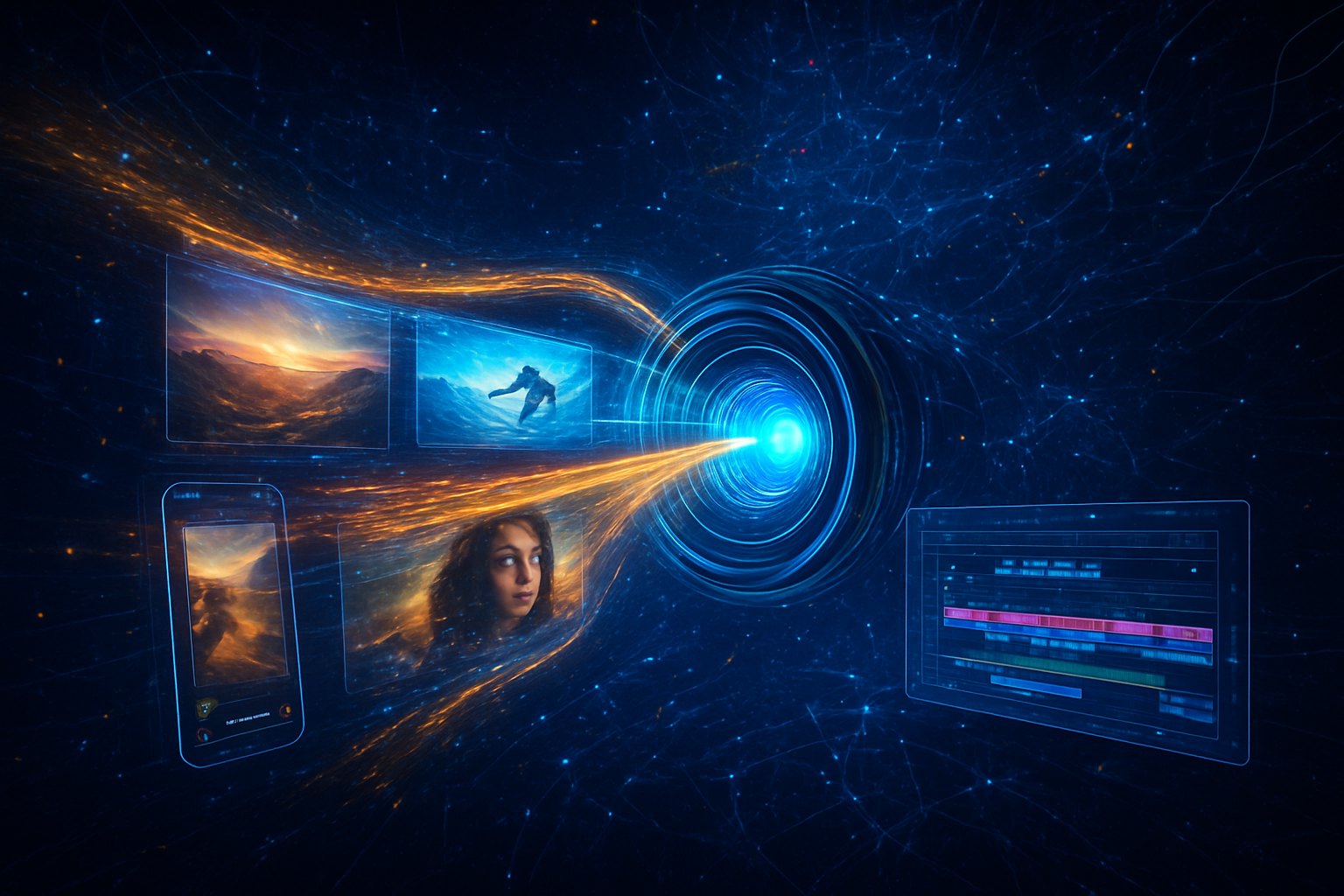
The significance of these statutes cannot be overstated. For the first time, the law explicitly distinguishes between a human performance and a "digital replica"—a computer-generated representation that mimics an individual’s voice or likeness so closely that it could be mistaken for the real person. While 2024 was defined by the anxiety of displacement, 2025 became the year of the "AI Rider," as every major studio and tech firm was forced to navigate the strictest likeness protections in the world.
The Technical and Legal Architecture of Protection
AB 2602 and AB 1836 represent a two-pronged defense strategy designed by SAG-AFTRA and California legislators to safeguard the labor and legacies of performers. AB 2602 targets the contracts of living performers, rendering "unconscionable" any agreement that allows a studio to create a digital replica without a "reasonably specific description" of its use. Crucially, it mandates that performers must be represented by legal counsel or a labor union when signing such deals. This ended the practice of "perpetual rights" clauses that once sought to own an actor’s digital soul "in all media now known or hereafter devised."
AB 1836, meanwhile, addresses the "digital resurrection" of deceased stars. It closed previous fair-use loopholes, requiring explicit consent from an estate before a digital replica of a deceased personality can be used in "expressive audiovisual works" or sound recordings. Technically, this law redefined the post-mortem right of publicity for the age of Sora and voice-cloning. By early 2026, the "Digital Replica" has been codified as a distinct legal asset, separate from traditional performance footage, requiring its own metadata and licensing chain. This differs from previous approaches which relied on vague "right of publicity" claims that were often toothless against transformative AI uses.
Initial reactions in early 2025 were mixed; while performers hailed it as a victory for human labor, some AI researchers argued that the broad definitions could stifle "background" AI technologies used for harmless post-production fixes. However, the industry quickly standardized these definitions, with the SAG-AFTRA Interactive Media Agreement ratified in July 2025 further cementing these protections into the fabric of video game development and voice acting.
Strategic Realignment: Disney, OpenAI, and the Tech Giants
The implementation of these laws has forced a massive strategic pivot for tech giants and major studios. The Walt Disney Company (NYSE: DIS) and Netflix, Inc. (NASDAQ: NFLX) spent much of 2025 overhauling their legal departments to ensure compliance. Instead of resisting the laws, many have opted for "compliance through partnership." In December 2025, Disney signed a landmark deal with OpenAI (backed by Microsoft (NASDAQ: MSFT)) to create a "walled garden" for authorized digital replicas. This deal allows Disney to use OpenAI’s advanced video models, like Sora, to generate replicas of its own intellectual property while maintaining a strictly controlled legal framework for revenue sharing—effectively turning AB 1836 from a hurdle into a monetization tool.
However, the competitive implications for other AI labs have been stark. Smaller startups have struggled with the "representation mandate" of AB 2602, as the cost of negotiating individual union-vetted contracts for AI training data is prohibitive. Meta Platforms, Inc. (NASDAQ: META) has been a vocal critic, arguing in early 2026 court filings that California’s specific protections create an "unconstitutional patchwork" that hinders American AI dominance. The disruption to existing services was most visible in the "Sora Backlash" of late 2025, where OpenAI was forced to implement "estate blocks" for figures like Robin Williams and Martin Luther King Jr. after their estates invoked AB 1836 to stop unauthorized viral clips.
Wider Significance: Ethics, Estates, and the Sora Backlash
Beyond the legal technicalities, AB 1836 and AB 2602 have become the ethical benchmark for the global AI landscape. The 2025 disputes involving the Williams and King estates highlighted the potential for AI to be used in "sycophantic" or politically motivated ways that dilute a performer’s lifelong brand. By empowering estates to act as "legacy guardians," California has set a precedent that is now being mirrored in international discussions at the EU AI Office. These laws are seen as a critical milestone in AI history, comparable to the first copyright protections for recorded music, marking the moment society decided that human identity is not mere "data" to be harvested.
Potential concerns remain, particularly regarding the First Amendment. Some legal experts argue that AB 1836’s restrictions on "expressive works" could inadvertently ban legitimate satire or documentary filmmaking. Throughout 2025, several "fan-made" AI comedy specials were scrubbed from platforms like YouTube (owned by Alphabet Inc. (NASDAQ: GOOGL)) following legal notices from the estates of deceased comedians like George Carlin. This tension between the "right to be forgotten" (or at least, the right not to be resurrected) and the freedom of expression is the primary battleground as we enter 2026.
The Horizon: Federal Preemption and the "NO FAKES" Era
Looking ahead, the near-term focus is no longer on Sacramento, but on Washington D.C. In December 2025, a new Executive Order was signed by President Trump, which led to the creation of a Department of Justice AI Litigation Task Force in January 2026. This task force has specifically identified California’s AB 1836 and AB 2602 as targets for federal preemption. The argument is that these state-level protections are "cumbersome" and violate the First Amendment by creating a prior restraint on digital creativity.
Experts predict that the "TRUMP AMERICA AI Act," currently being debated in early 2026, may attempt to nullify California’s specific performer protections in favor of a more "pro-innovation" federal standard. Meanwhile, the entertainment industry is keeping a close eye on the NO FAKES Act, a bipartisan federal bill that many hope will create a uniform national standard, potentially absorbing the best parts of California’s laws while providing a clearer path for tech companies to operate across state lines.
Summary: A Turning Point for Digital Identity
The first year of AB 2602 and AB 1836 has been a masterclass in the power of collective bargaining and legislative foresight. SAG-AFTRA’s leadership turned a moment of technological crisis into a permanent legal safeguard, ensuring that the human element remains at the heart of storytelling. The key takeaway from early 2026 is that while AI can replicate a voice or a face, the legal "right" to that identity remains firmly in human hands—at least in California.
As we move further into 2026, the industry should watch for the Supreme Court's potential involvement in the preemption battles and the outcome of the DOJ’s challenge to California’s authority. The "Digital Replica" laws have proven that regulation can coexist with innovation, as seen in the Disney-OpenAI partnership, but the tug-of-war between state-level labor protections and federal AI ambitions is only just beginning.
This content is intended for informational purposes only and represents analysis of current AI developments.
TokenRing AI delivers enterprise-grade solutions for multi-agent AI workflow orchestration, AI-powered development tools, and seamless remote collaboration platforms.
For more information, visit https://www.tokenring.ai/.