Blog

  • The Silicon Brain: How Next-Gen AI Chips Are Rewriting the Future of Intelligence

    The Silicon Brain: How Next-Gen AI Chips Are Rewriting the Future of Intelligence

    The artificial intelligence revolution, once primarily a software-driven phenomenon, is now being fundamentally reshaped by a parallel transformation in hardware. As traditional processors hit their architectural limits, a new era of AI chip architecture is dawning. This shift is characterized by innovative designs and specialized accelerators that promise to unlock unprecedented AI capabilities with immediate and profound impact, moving beyond the general-purpose computing paradigms that have long dominated the tech landscape. These advancements are not just making AI faster; they are making it smarter, more efficient, and capable of operating in ways previously thought impossible, signaling a critical juncture in the development of artificial intelligence.

    Unpacking the Architectural Revolution: Specialized Silicon for a Smarter Future

    The future of AI chip architecture is rapidly evolving, driven by the increasing demand for computational power, energy efficiency, and real-time processing required by complex AI models. This evolution is moving beyond traditional CPU and GPU architectures towards specialized accelerators and innovative designs, with the global AI hardware market projected to reach $210.50 billion by 2034. Experts believe that the next phase of AI breakthroughs will be defined by hardware innovation, not solely by larger software models, prioritizing faster, more efficient, and scalable chips, often adopting multi-component, heterogeneous systems where each component is engineered for a specific function within a single package.

    At the forefront of this revolution are groundbreaking designs that fundamentally rethink how computation and memory interact. Neuromorphic computing, for instance, draws inspiration from the human brain, utilizing "spiking neural networks" (SNNs) to process information. Unlike traditional processors that execute instructions sequentially or in parallel with predefined instructions, these chips are event-driven, activating only when new information is detected, much like biological neurons communicate through discrete electrical spikes. This brain-inspired approach, exemplified by Intel (NASDAQ: INTC)'s Hala Point, which uses over 1,000 Loihi 2 processors, offers exceptional energy efficiency, real-time processing, and adaptability, enabling AI to learn dynamically on the device. Initial prototypes have shown performing AI workloads 50 times faster and using 100 times less energy than conventional systems.

    Another significant innovation is In-Memory Computing (IMC), which directly tackles the "von Neumann bottleneck"—the inefficiency caused by data constantly shuffling between the processor and separate memory units. IMC integrates computation directly within or adjacent to memory units, drastically reducing data transfer delays and power consumption. This approach is particularly promising for large AI models and compact edge devices, offering significant improvements in AI costs, reduced compute time, and lower power usage, especially for inference applications. Complementing this, 3D Stacking (or 3D packaging) involves vertically integrating multiple semiconductor dies. This allows for massive and fast data movement by shortening interconnect distances, bypassing bottlenecks inherent in flat, 2D designs, and offering substantial improvements in performance and energy efficiency. Companies like AMD (NASDAQ: AMD) with its 3D V-Cache and Intel (NASDAQ: INTC) with Foveros technology are already implementing these advancements, with early prototypes demonstrating performance gains of roughly an order of magnitude over comparable 2D chips.

    These innovative designs are coupled with a new generation of specialized AI accelerators. While Graphics Processing Units (GPUs) from NVIDIA (NASDAQ: NVDA) were revolutionary for parallel AI workloads, dedicated AI chips are taking specialization to the next level. Neural Processing Units (NPUs) are specifically engineered from the ground up for neural network computations, delivering superior performance and energy efficiency, especially for edge computing. Google (NASDAQ: GOOGL)'s Tensor Processing Units (TPUs) are a prime example of custom Application-Specific Integrated Circuits (ASICs), meticulously designed for machine learning tasks. TPUs, now in their seventh generation (Ironwood), feature systolic array architectures and high-bandwidth memory (HBM), capable of performing 16K multiply-accumulate operations per cycle in their latest versions, significantly accelerating AI workloads across Google services. Custom ASICs offer the highest level of optimization, often delivering 10 to 100 times greater energy efficiency compared to GPUs for specific AI tasks, although they come with less flexibility and higher initial design costs. The AI research community and industry experts widely acknowledge the critical role of this specialized hardware, recognizing that future AI breakthroughs will increasingly depend on such infrastructure, not solely on software advancements.

    Reshaping the Corporate Landscape: Who Wins in the AI Silicon Race?

    The advent of advanced AI chip architectures is profoundly impacting the competitive landscape across AI companies, tech giants, and startups, driving a strategic shift towards vertical integration and specialized solutions. This silicon arms race is poised to redefine market leadership and disrupt existing product and service offerings.

    Tech giants are strategically positioned to benefit immensely due to their vast resources and established ecosystems. Companies like Google (NASDAQ: GOOGL), Amazon (NASDAQ: AMZN), Microsoft (NASDAQ: MSFT), and Meta (NASDAQ: META) are heavily investing in developing their own custom AI silicon. Google's TPUs, Amazon Web Services (AWS)'s Trainium and Inferentia chips, Microsoft's Azure Maia 100 and Azure Cobalt 100, and Meta's MTIA are all examples of this vertical integration strategy. By designing their own chips, these companies aim to optimize performance for specific workloads, reduce reliance on third-party suppliers like NVIDIA (NASDAQ: NVDA), and achieve significant cost efficiencies, particularly for AI inference tasks. This move allows them to differentiate their cloud offerings and internal AI services, gaining tighter control over their hardware and software stacks.

    The competitive implications for major AI labs and tech companies are substantial. There's a clear trend towards reduced dependence on NVIDIA's dominant GPUs, especially for AI inference, where custom ASICs can offer lower power consumption and cost. This doesn't mean NVIDIA is out of the game; they continue to lead the AI training market and are exploring advanced packaging like 3D stacking and silicon photonics. However, the rise of custom silicon forces NVIDIA and AMD (NASDAQ: AMD), which is expanding its AI capabilities with products like the MI300 series, to innovate rapidly and offer more specialized, high-performance solutions. The ability to offer AI solutions with superior energy efficiency and lower latency will be a key differentiator, with neuromorphic and in-memory computing excelling in this regard, particularly for edge devices where power constraints are critical.

    This architectural shift also brings potential disruption to existing products and services. The enhanced efficiency of neuromorphic computing, in-memory computing, and NPUs enables more powerful AI processing directly on devices, reducing the need for constant cloud connectivity. This could disrupt cloud-based AI service models, especially for real-time, privacy-sensitive, or low-power applications. Conversely, it could also lead to the democratization of AI, lowering the barrier to entry for AI development by making sophisticated AI systems more accessible and cost-effective. The focus will shift from general-purpose computing to workload-specific optimization, with systems integrating multiple processor types (GPUs, CPUs, NPUs, TPUs) for different tasks, potentially disrupting traditional hardware sales models.

    For startups, this specialized landscape presents both challenges and opportunities. Startups focused on niche hardware or specific AI applications can thrive by providing highly optimized solutions that fill gaps left by general-purpose hardware. For instance, neuromorphic computing startups like BrainChip, Rain Neuromorphics, and GrAI Matter Labs are developing energy-efficient chips for edge AI, robotics, and smart sensors. Similarly, in-memory computing startups like TensorChip and Axelera AI are creating chips for high throughput and low latency at the edge. Semiconductor foundries like TSMC (NYSE: TSM) and Samsung (KRX: 005930), along with IP providers like Marvell (NASDAQ: MRVL) and Broadcom (NASDAQ: AVGO), are crucial enablers, providing the advanced manufacturing and design expertise necessary for these complex architectures. Their mastery of 3D stacking and other advanced packaging techniques will make them essential partners and leaders in delivering the next generation of high-performance AI chips.

    A Broader Canvas: AI Chips and the Future of Society

    The future of AI chip architecture is not just a technical evolution; it's a societal one, deeply intertwined with the broader AI landscape and trends. These advancements are poised to enable unprecedented levels of performance, efficiency, and capability, promising profound impacts across society and various industries, while also presenting significant concerns that demand careful consideration.

    These advanced chip architectures directly address the escalating computational demands and inefficiencies of modern AI. The "memory wall" in traditional von Neumann architectures and the skyrocketing energy costs of training large AI models are major concerns that specialized chips are designed to overcome. The shift towards these architectures signifies a move towards more pervasive, responsive, and efficient intelligence, enabling the proliferation of AI at the "edge"—on devices like IoT sensors, smartphones, and autonomous vehicles—where real-time processing, low power consumption, and data security are paramount. This decentralization of AI capabilities is a significant trend, comparable to the shift from mainframes to personal computing or the rise of cloud computing, democratizing access to powerful computational resources.

    The impacts on society and industries are expected to be transformative. In healthcare, faster and more accurate AI processing will enable early disease diagnosis, personalized medicine, and accessible telemedicine. Autonomous vehicles, drones, and advanced robotics will benefit from real-time decision-making, enhancing safety and efficiency. Cybersecurity will see neuromorphic chips continuously learning from network traffic patterns to detect new and evolving threats with low latency. In manufacturing, advanced robots and optimized industrial processes will become more adaptable and efficient. For consumer electronics, supercomputer-level performance could be integrated into compact devices, powering highly responsive AI assistants and advanced functionalities. Crucially, improved efficiency and reduced power consumption in data centers will be critical for scaling AI operations, leading to lower operational costs and potentially making AI solutions more accessible to developers with limited resources.

    Despite the immense potential, the future of AI chip architecture raises several critical concerns. While newer architectures aim for significant energy efficiency, the sheer scale of AI development still demands immense computational resources, contributing to a growing carbon footprint and straining power grids. This raises ethical questions about the environmental impact and the perpetuation of societal inequalities if AI development is not powered by renewable sources or if biased models are deployed. Ensuring ethical AI development requires addressing issues like data quality, fairness, and the potential for algorithmic bias. The increased processing of sensitive data at the edge also raises privacy concerns that must be managed through secure enclaves and robust data protection. Furthermore, the high cost of developing and deploying high-performance AI accelerators could create a digital divide, although advancements in AI-driven chip design could eventually reduce costs. Other challenges include thermal management for densely packed 3D-stacked chips, the need for new software compatibility and development frameworks, and the rapid iteration of hardware contributing to e-waste.

    This architectural evolution is as significant as, if not more profound than, previous AI milestones. The initial AI revolution was fueled by the adaptation of GPUs, overcoming the limitations of general-purpose CPUs. The current emergence of specialized hardware, neuromorphic designs, and in-memory computing moves beyond simply shrinking transistors, fundamentally re-architecting how AI operates. This enables improvements in performance and efficiency that are orders of magnitude greater than what traditional scaling could achieve alone, with some comparing the leap in performance to an improvement equivalent to 26 years of Moore's Law-driven CPU advancements for AI tasks. This represents a decentralization of intelligence, making AI more ubiquitous and integrated into our physical environment.

    The Horizon: What's Next for AI Silicon?

    The relentless pursuit of speed, efficiency, and specialization continues to drive the future developments in AI chip architecture, promising to unlock new frontiers in artificial intelligence. Both near-term enhancements and long-term revolutionary paradigms are on the horizon, addressing current limitations and enabling unprecedented applications.

    In the near term (next 1-5 years), advancements will focus on enhancing existing technologies through sophisticated integration methods. Advanced packaging and heterogeneous integration will become the norm, moving towards modular, chiplet-based architectures. Companies like NVIDIA (NASDAQ: NVDA) with its Blackwell architecture, AMD (NASDAQ: AMD) with its MI300 series, and hyperscalers like Google (NASDAQ: GOOGL) with TPU v6 and Amazon (NASDAQ: AMZN) with Trainium 2 are already leveraging multi-die GPU modules and High-Bandwidth Memory (HBM) to achieve exponential gains. Research indicates that these 3D chips can significantly outperform 2D chips, potentially leading to 100- to 1,000-fold improvements in energy-delay product. Specialized accelerators (ASICs and NPUs) will become even more prevalent, with a continued focus on energy efficiency through optimized power consumption features and specialized circuit designs, crucial for both data centers and edge devices.

    Looking further ahead into the long term (beyond 5 years), revolutionary computing paradigms are being explored to overcome the fundamental limits of silicon-based electronics. Optical computing, which uses light (photons) instead of electricity, promises extreme processing speed, reduced energy consumption, and high parallelism, particularly well-suited for the linear algebra operations central to AI. Hybrid architectures combining photonic accelerators with digital processors are expected to become mainstream over the next decade, with the optical processors market forecasted to reach US$3 billion by 2034. Neuromorphic computing will continue to evolve, aiming for ultra-low-power AI systems capable of continuous learning and adaptation, fundamentally moving beyond the traditional Von Neumann architecture bottlenecks. The most speculative, yet potentially transformative, development lies in Quantum AI Chips. By leveraging quantum-mechanical phenomena, these chips hold immense promise for accelerating machine learning, optimization, and simulation tasks that are intractable for classical computers. The convergence of AI chips and quantum computing is expected to lead to breakthroughs in areas like drug discovery, climate modeling, and cybersecurity, with the quantum optical computer market projected to reach US$300 million by 2034.

    These advanced architectures will unlock a new generation of sophisticated AI applications. Even larger and more complex Large Language Models (LLMs) and generative AI models will be trained and inferred, leading to more human-like text generation and advanced content creation. Autonomous systems (self-driving cars, robotics, drones) will benefit from real-time decision-making, object recognition, and navigation powered by specialized edge AI chips. The proliferation of Edge AI will enable sophisticated AI capabilities directly on smartphones and IoT devices, supporting applications like facial recognition and augmented reality. Furthermore, High-Performance Computing (HPC) and scientific research will be accelerated, impacting fields such as drug discovery and climate modeling.

    However, significant challenges must be addressed. Manufacturing complexity and cost for advanced semiconductors, especially at smaller process nodes, remain immense. The projected power consumption and heat generation of next-generation AI chips, potentially exceeding 15,000 watts per unit by 2035, demand fundamental changes in data center infrastructure and cooling systems. The memory wall and energy associated with data movement continue to be major hurdles, with optical interconnects being explored as a solution. Software integration and development frameworks for novel architectures like optical and quantum computing are still nascent. For quantum AI chips, qubit fragility, short coherence times, and scalability issues are significant technical hurdles. Experts predict a future shaped by hybrid architectures, combining the strengths of different computing paradigms, and foresee AI itself becoming instrumental in designing and optimizing future chips. While NVIDIA (NASDAQ: NVDA) is expected to maintain its dominance in the medium term, competition from AMD (NASDAQ: AMD) and custom ASICs will intensify, with optical computing anticipated to become a mainstream solution for data centers by 2027/2028.

    The Dawn of Specialized Intelligence: A Concluding Assessment

    The ongoing transformation in AI chip architecture marks a pivotal moment in the history of artificial intelligence, heralding a future where specialized, highly efficient, and increasingly brain-inspired designs are the norm. The key takeaway is a definitive shift away from the general-purpose computing paradigms that once constrained AI's potential. This architectural revolution is not merely an incremental improvement but a fundamental reshaping of how AI is built and deployed, promising to unlock unprecedented capabilities and integrate intelligence seamlessly into our world.

    This development's significance in AI history cannot be overstated. Just as the adaptation of GPUs catalyzed the deep learning revolution, the current wave of specialized accelerators, neuromorphic computing, and advanced packaging techniques is enabling the training and deployment of AI models that were once computationally intractable. This hardware innovation is the indispensable backbone of modern AI breakthroughs, from advanced natural language processing to computer vision and autonomous systems, making real-time, intelligent decision-making possible across various industries. Without these purpose-built chips, sophisticated AI algorithms would remain largely theoretical, making this architectural shift fundamental to AI's practical realization and continued progress.

    The long-term impact will be transformative, leading to ubiquitous and pervasive AI embedded into nearly every device and system, from tiny IoT sensors to advanced robotics. This will enable enhanced automation and new capabilities across healthcare, manufacturing, finance, and automotive, fostering decentralized intelligence and hybrid AI infrastructures. However, this future also necessitates a rethinking of data center design and sustainability, as the rising power demands of next-gen AI chips will require fundamental changes in infrastructure and cooling. The geopolitical landscape around semiconductor manufacturing will also continue to be a critical factor, influencing chip availability and market dynamics.

    In the coming weeks and months, watch for continuous advancements in chip efficiency and novel architectures, particularly in neuromorphic computing and heterogeneous integration. The emergence of specialized chips for generative AI and LLMs at the edge will be a critical indicator of future capabilities, enabling more natural and private user experiences. Keep an eye on new software tools and platforms that simplify the deployment of complex AI models on these specialized chipsets, as their usability will be key to widespread adoption. The competitive landscape among established semiconductor giants and innovative AI hardware startups will continue to drive rapid advancements, especially in HBM-centric computing and thermal management solutions. Finally, monitor the evolving global supply chain dynamics and the trend of shifting AI model training to "thick edge" servers, as these will directly influence the pace and direction of AI hardware development. The future of AI is undeniably intertwined with the future of its underlying silicon, promising an era of specialized intelligence that will redefine our technological capabilities.


    This content is intended for informational purposes only and represents analysis of current AI developments.

    TokenRing AI delivers enterprise-grade solutions for multi-agent AI workflow orchestration, AI-powered development tools, and seamless remote collaboration platforms.
    For more information, visit https://www.tokenring.ai/.

  • Beyond Silicon: How Advanced Materials and 3D Packaging Are Revolutionizing AI Chips

    Beyond Silicon: How Advanced Materials and 3D Packaging Are Revolutionizing AI Chips

    The insatiable demand for ever-increasing computational power and efficiency in Artificial Intelligence (AI) applications is pushing the boundaries of traditional silicon-based semiconductor manufacturing. As the industry grapples with the physical limits of transistor scaling, a new era of innovation is dawning, driven by groundbreaking advancements in semiconductor materials and sophisticated advanced packaging techniques. These emerging technologies, including 3D packaging, chiplets, and hybrid bonding, are not merely incremental improvements; they represent a fundamental shift in how AI chips are designed and fabricated, promising unprecedented levels of performance, power efficiency, and functionality.

    These innovations are critical for powering the next generation of AI, from colossal large language models (LLMs) in hyperscale data centers to compact, energy-efficient AI at the edge. By enabling denser integration, faster data transfer, and superior thermal management, these advancements are poised to accelerate AI development, unlock new capabilities, and reshape the competitive landscape of the global technology industry. The convergence of novel materials and advanced packaging is set to be the cornerstone of future AI breakthroughs, addressing bottlenecks that traditional methods can no longer overcome.

    The Architectural Revolution: 3D Stacking, Chiplets, and Hybrid Bonding Unleashed

    The core of this revolution lies in moving beyond the flat, monolithic chip design to a three-dimensional, modular architecture. This paradigm shift involves several key technical advancements that work in concert to enhance AI chip performance and efficiency dramatically.

    3D Packaging, encompassing 2.5D and true vertical stacking, is at the forefront. Instead of placing components side-by-side on a large, expensive silicon die, chips are stacked vertically, drastically shortening the physical distance data must travel between compute units and memory. This directly translates to vastly increased memory bandwidth and significantly reduced latency – two critical factors for AI workloads, which are often memory-bound and require rapid access to massive datasets. Companies like TSMC (NYSE: TSM) are leaders in this space with their CoWoS (Chip-on-Wafer-on-Substrate) technology, a 2.5D packaging solution widely adopted for high-performance AI accelerators such as NVIDIA's (NASDAQ: NVDA) H100. Intel (NASDAQ: INTC) is also heavily invested with Foveros (3D stacking) and EMIB (Embedded Multi-die Interconnect Bridge), while Samsung (KRX: 005930) offers I-Cube (2.5D) and X-Cube (3D stacking) platforms.

    Complementing 3D packaging are Chiplets, a modular design approach where a complex System-on-Chip (SoC) is disaggregated into smaller, specialized "chiplets" (e.g., CPU, GPU, memory, I/O, AI accelerators). These chiplets are then integrated into a single package using advanced packaging techniques. This offers unparalleled flexibility, allowing designers to mix and match different chiplets, each manufactured on the most optimal (and cost-effective) process node for its specific function. This heterogeneous integration is particularly beneficial for AI, enabling the creation of highly customized accelerators tailored for specific workloads. AMD (NASDAQ: AMD) has been a pioneer in this area, utilizing chiplets with 3D V-cache in its Ryzen processors and integrating CPU/GPU tiles in its Instinct MI300 series.

    The glue that binds these advanced architectures together is Hybrid Bonding. This cutting-edge direct copper-to-copper (Cu-Cu) bonding technology creates ultra-dense vertical interconnections between dies or wafers at pitches below 10 µm, even approaching sub-micron levels. Unlike traditional methods that rely on solder or intermediate materials, hybrid bonding forms direct metal-to-metal connections, dramatically increasing I/O density and bandwidth while minimizing parasitic capacitance and resistance. This leads to lower latency, reduced power consumption, and improved thermal conduction, all vital for the demanding power and thermal requirements of AI chips. IBM Research and ASMPT have achieved significant milestones, pushing interconnection sizes to around 0.8 microns, enabling over 1000 GB/s bandwidth with high energy efficiency.

    These advancements represent a significant departure from the monolithic chip design philosophy. Previous approaches focused primarily on shrinking transistors on a single die (Moore's Law). While transistor scaling remains important, advanced packaging and chiplets offer a new dimension of performance scaling by optimizing inter-chip communication and allowing for heterogeneous integration. The initial reactions from the AI research community and industry experts are overwhelmingly positive, recognizing these techniques as essential for sustaining the pace of AI innovation. They are seen as crucial for breaking the "memory wall" and enabling the power-efficient processing required for increasingly complex AI models.

    Reshaping the AI Competitive Landscape

    These emerging trends in semiconductor materials and advanced packaging are poised to profoundly impact AI companies, tech giants, and startups alike, creating new competitive dynamics and strategic advantages.

    NVIDIA (NASDAQ: NVDA), a dominant player in AI hardware, stands to benefit immensely. Their cutting-edge GPUs, like the H100, already leverage TSMC's CoWoS 2.5D packaging to integrate the GPU die with high-bandwidth memory (HBM). As 3D stacking and hybrid bonding become more prevalent, NVIDIA can further optimize its accelerators for even greater performance and efficiency, maintaining its lead in the AI training and inference markets. The ability to integrate more specialized AI acceleration chiplets will be key.

    Intel (NASDAQ: INTC), is strategically positioning itself to regain market share in the AI space through its robust investments in advanced packaging technologies like Foveros and EMIB. By leveraging these capabilities, Intel aims to offer highly competitive AI accelerators and CPUs that integrate diverse computing elements, challenging NVIDIA and AMD. Their foundry services, offering these advanced packaging options to third parties, could also become a significant revenue stream and influence the broader ecosystem.

    AMD (NASDAQ: AMD) has already demonstrated its prowess with chiplet-based designs in its CPUs and GPUs, particularly with its Instinct MI300 series, which combines CPU and GPU elements with HBM using advanced packaging. Their early adoption and expertise in chiplets give them a strong competitive edge, allowing for flexible, cost-effective, and high-performance solutions tailored for various AI workloads.

    Foundries like TSMC (NYSE: TSM) and Samsung (KRX: 005930) are critical enablers. Their continuous innovation and expansion of advanced packaging capacities are essential for the entire AI industry. Their ability to provide cutting-edge packaging services will determine who can bring the most performant and efficient AI chips to market. The competition between these foundries to offer the most advanced 2.5D/3D integration and hybrid bonding capabilities will be fierce.

    Beyond the major chip designers, companies specializing in advanced materials like Wolfspeed (NYSE: WOLF), Infineon (FSE: IFX), and Navitas Semiconductor (NASDAQ: NVTS) are becoming increasingly vital. Their wide-bandgap materials (SiC and GaN) are crucial for power management in AI data centers, where power efficiency is paramount. Startups focusing on novel 2D materials or specialized chiplet designs could also find niches, offering custom solutions for emerging AI applications.

    The potential disruption to existing products and services is significant. Monolithic chip designs will increasingly struggle to compete with the performance and efficiency offered by advanced packaging and chiplets, particularly for demanding AI tasks. Companies that fail to adopt these architectural shifts risk falling behind. Market positioning will increasingly depend not just on transistor technology but also on expertise in heterogeneous integration, thermal management, and robust supply chains for advanced packaging.

    Wider Significance and Broad AI Impact

    These advancements in semiconductor materials and advanced packaging are more than just technical marvels; they represent a pivotal moment in the broader AI landscape, addressing fundamental limitations and paving the way for unprecedented capabilities.

    Foremost, these innovations are directly addressing the slowdown of Moore's Law. While transistor density continues to increase, the rate of performance improvement per dollar has decelerated. Advanced packaging offers a "More than Moore" solution, providing performance gains by optimizing inter-component communication and integration rather than solely relying on transistor shrinks. This allows for continued progress in AI chip capabilities even as the physical limits of silicon are approached.

    The impact on AI development is profound. The ability to integrate high-bandwidth memory directly with compute units in 3D stacks, enabled by hybrid bonding, is crucial for training and deploying increasingly massive AI models, such as large language models (LLMs) and complex generative AI architectures. These models demand vast amounts of data to be moved quickly between processors and memory, a bottleneck that traditional packaging struggles to overcome. Enhanced power efficiency from wide-bandgap materials and optimized chip designs also makes AI more sustainable and cost-effective to operate at scale.

    Potential concerns, however, are not negligible. The complexity of designing, manufacturing, and testing 3D stacked chips and chiplet systems is significantly higher than monolithic designs. This can lead to increased development costs, longer design cycles, and new challenges in thermal management, as stacking chips generates more localized heat. Supply chain complexities also multiply, requiring tighter collaboration between chip designers, foundries, and outsourced assembly and test (OSAT) providers. The cost of advanced packaging itself can be substantial, potentially limiting its initial adoption to high-end AI applications.

    Comparing this to previous AI milestones, this architectural shift is as significant as the advent of GPUs for parallel processing or the development of specialized AI accelerators like TPUs. It's a foundational change that enables the next wave of algorithmic breakthroughs by providing the necessary hardware substrate. It moves beyond incremental improvements to a systemic rethinking of chip design, akin to the transition from single-core to multi-core processors, but with an added dimension of vertical integration and modularity.

    The Road Ahead: Future Developments and Challenges

    The trajectory for these emerging trends points towards even more sophisticated integration and specialized materials, with significant implications for future AI applications.

    In the near term, we can expect to see wider adoption of 2.5D and 3D packaging across a broader range of AI accelerators, moving beyond just the highest-end data center chips. Hybrid bonding will become increasingly common for integrating memory and compute, pushing interconnect densities even further. The UCIe (Universal Chiplet Interconnect Express) standard will gain traction, fostering a more open and interoperable chiplet ecosystem, allowing companies to mix and match chiplets from different vendors. This will drive down costs and accelerate innovation by democratizing access to specialized IP.

    Long-term developments include the deeper integration of novel materials. While 2D materials like graphene and molybdenum disulfide are still primarily in research, breakthroughs in fabricating semiconducting graphene with useful bandgaps suggest future possibilities for ultra-thin, high-mobility transistors that could be heterogeneously integrated with silicon. Silicon Carbide (SiC) and Gallium Nitride (GaN) will continue to mature, not just for power electronics but potentially for high-frequency AI processing at the edge, enabling extremely compact and efficient AI devices for IoT and mobile applications. We might also see the integration of optical interconnects within 3D packages to further reduce latency and increase bandwidth for inter-chiplet communication.

    Challenges remain formidable. Thermal management in densely packed 3D stacks is a critical hurdle, requiring innovative cooling solutions and thermal interface materials. Ensuring manufacturing yield and reliability for complex multi-chiplet, 3D stacked systems is another significant engineering task. Furthermore, the development of robust design tools and methodologies that can efficiently handle the complexities of heterogeneous integration and 3D layout is essential.

    Experts predict that the future of AI hardware will be defined by highly specialized, heterogeneously integrated systems, meticulously optimized for specific AI workloads. This will move away from general-purpose computing towards purpose-built AI engines. The emphasis will be on system-level performance, power efficiency, and cost-effectiveness, with packaging becoming as important as the transistors themselves. What experts predict is a future where AI accelerators are not just faster, but also smarter in how they manage and move data, driven by these architectural and material innovations.

    A New Era for AI Hardware

    The convergence of emerging semiconductor materials and advanced packaging techniques marks a transformative period for AI hardware. The shift from monolithic silicon to modular, three-dimensional architectures utilizing chiplets, 3D stacking, and hybrid bonding, alongside the exploration of wide-bandgap and 2D materials, is fundamentally reshaping the capabilities of AI chips. These innovations are critical for overcoming the limitations of traditional transistor scaling, providing the unprecedented bandwidth, lower latency, and improved power efficiency demanded by today's and tomorrow's sophisticated AI models.

    The significance of this development in AI history cannot be overstated. It is a foundational change that enables the continued exponential growth of AI capabilities, much like the invention of the transistor itself or the advent of parallel computing with GPUs. It signifies a move towards a more holistic, system-level approach to chip design, where packaging is no longer a mere enclosure but an active component in enhancing performance.

    In the coming weeks and months, watch for continued announcements from major foundries and chip designers regarding expanded advanced packaging capacities and new product launches leveraging these technologies. Pay close attention to the development of open chiplet standards and the increasing adoption of hybrid bonding in commercial products. The success in tackling thermal management and manufacturing complexity will be key indicators of how rapidly these advancements proliferate across the AI ecosystem. This architectural revolution is not just about building faster chips; it's about building the intelligent infrastructure for the future of AI.


    This content is intended for informational purposes only and represents analysis of current AI developments.

    TokenRing AI delivers enterprise-grade solutions for multi-agent AI workflow orchestration, AI-powered development tools, and seamless remote collaboration platforms.
    For more information, visit https://www.tokenring.ai/.

  • Cohu, Inc. Navigates Semiconductor Downturn with Strategic Focus on AI and Advanced Chip Quality Assurance

    Cohu, Inc. Navigates Semiconductor Downturn with Strategic Focus on AI and Advanced Chip Quality Assurance

    Cohu, Inc. (NASDAQ: COHU), a global leader in semiconductor test and inspection solutions, is demonstrating remarkable resilience and strategic foresight amidst a challenging cyclical downturn in the semiconductor industry. While recent financial reports reflect the broader market's volatility, Cohu's unwavering commitment to innovation in chip quality assurance, particularly in high-growth areas like Artificial Intelligence (AI) and High Bandwidth Memory (HBM) testing, underscores its critical importance to the future of technology. The company's strategic initiatives, including key acquisitions and new product launches, are not only bolstering its market position but also ensuring the reliability and performance of the next generation of semiconductors that power our increasingly AI-driven world.

    Cohu's indispensable role lies in providing the essential equipment and services that optimize semiconductor manufacturing yield and productivity. From advanced test handlers and burn-in equipment to sophisticated inspection and metrology platforms, Cohu’s technologies are the bedrock upon which chip manufacturers build trust in their products. As the demand for flawless, high-performance chips escalates across automotive, industrial, and data center sectors, Cohu's contributions to rigorous testing and defect detection are more vital than ever, directly impacting the quality and longevity of electronic devices globally.

    Precision Engineering for Flawless Silicon: Cohu's Technical Edge in Chip Verification

    Cohu's technological prowess is evident in its suite of advanced solutions designed to meet the escalating demands for chip quality and reliability. At the heart of its offerings are high-precision test and handling systems, which include sophisticated pick-and-place semiconductor test handlers, burn-in equipment, and thermal sub-systems. These systems are not merely components in a production line; they are critical gatekeepers, rigorously testing chips under diverse and extreme conditions to identify even the most minute defects and ensure flawless functionality before they reach end-user applications.

    A significant advancement in Cohu's portfolio is the Krypton inspection and metrology platform, launched in May 2024. This system represents a leap forward in optical inspection, capable of detecting defects as small as 1 µm with enhanced throughput and uptime. Its introduction is particularly timely, addressing the increasing quality demands from the automotive and industrial markets where even microscopic flaws can have catastrophic consequences. The Krypton platform has already secured an initial design-win, projecting an estimated $100 million revenue opportunity over the next five years. Furthermore, Cohu's Neon HBM inspection systems are gaining significant traction in the rapidly expanding AI data center markets, where the integrity of high-bandwidth memory is paramount for AI accelerators. The company projects these solutions to generate $10-$11 million in revenue in 2025, highlighting their direct relevance to the AI boom.

    Cohu differentiates itself from previous approaches and existing technologies through its integrated approach to thermal management and data analytics. The Eclipse platform, for instance, incorporates T-Core Active Thermal Control, providing precise thermal management up to an impressive 3kW dissipation with rapid ramp rates. This capability is crucial for testing high-performance devices, where temperature fluctuations can significantly impact test repeatability and overall yield. By ensuring stable and precise thermal environments, Eclipse improves the accuracy of testing and lowers the total cost of ownership for manufacturers. Complementing its hardware, Cohu's DI-Core™ Data Analytics suite offers real-time online performance monitoring and process control. This software platform is a game-changer, improving equipment utilization, enabling predictive maintenance, and integrating data from testers, handlers, and test contactors. Such integrated analytics are vital for identifying and resolving quality issues proactively, preventing significant production losses and safeguarding reputations in a highly competitive market. Initial reactions from the AI research community and industry experts emphasize the growing need for such robust, integrated test and inspection solutions, especially as chip complexity and performance demands continue to soar with the proliferation of AI.

    Cohu's Strategic Edge: Fueling the AI Revolution and Reshaping the Semiconductor Landscape

    Cohu's strategic advancements in semiconductor test and inspection are poised to significantly benefit a wide array of companies, particularly those at the forefront of the Artificial Intelligence revolution and high-performance computing. Chip designers like NVIDIA (NASDAQ: NVDA), AMD (NASDAQ: AMD), and Intel (NASDAQ: INTC), who are constantly pushing the boundaries of AI chip performance, stand to gain immensely from Cohu's enhanced quality assurance technologies. Their ability to deliver flawless, high-bandwidth memory and advanced processors directly relies on the precision and reliability of testing solutions like Cohu's Neon HBM inspection systems and the Eclipse platform. Furthermore, contract manufacturers and foundries such as TSMC (NYSE: TSM) and Samsung (KRX: 005930) will leverage Cohu's equipment to optimize their production yields and maintain stringent quality controls for their diverse client base, including major tech giants.

    The competitive implications for major AI labs and tech companies are substantial. As AI models become more complex and demand greater computational power, the underlying hardware must be impeccably reliable. Companies that can consistently source or produce higher-quality, more reliable AI chips will gain a significant competitive advantage in terms of system performance, energy efficiency, and overall innovation velocity. Cohu's offerings, by minimizing chip defects and ensuring optimal performance, directly contribute to this advantage. This development could potentially disrupt existing products or services that rely on less rigorous testing protocols, pushing the entire industry towards higher quality standards.

    In terms of market positioning and strategic advantages, Cohu is actively carving out a niche in the most critical and fastest-growing segments of the semiconductor market. Its acquisition of Tignis, Inc. in January 2025, a provider of AI process control and analytics software, is a clear strategic move to expand its analytics offerings and integrate AI directly into its quality control solutions. This acquisition is expected to significantly boost Cohu's software revenue, projecting 50% or more annual growth over the next three years. By focusing on AI and HBM testing, as well as the silicon carbide (SiC) markets driven by electric vehicles and renewable energy, Cohu is aligning itself with the mega-trends shaping the future of technology. Its recurring revenue model, comprising consumables, services, and software subscriptions, provides a stable financial base, acting as a crucial buffer against the inherent volatility of the semiconductor industry cycle and solidifying its strategic advantage.

    Cohu's Role in the Broader AI Landscape: Setting New Standards for Reliability

    Cohu's advancements in semiconductor test and inspection are not merely incremental improvements; they represent a fundamental strengthening of the foundation upon which the broader AI landscape is being built. As AI models become more sophisticated and pervasive, from autonomous vehicles to advanced robotics and enterprise-grade cloud computing, the demand for absolutely reliable and high-performance silicon is paramount. Cohu's technologies fit perfectly into this trend by ensuring that the very building blocks of AI – the processors, memory, and specialized accelerators – meet the highest standards of quality and functionality. This proactive approach to chip quality is critical, as even minor defects in AI hardware can lead to significant computational errors, system failures, and substantial financial losses, thereby impacting the trustworthiness and widespread adoption of AI solutions.

    The impacts of Cohu's work extend beyond just performance; they touch upon safety and ethical considerations in AI. For instance, in safety-critical applications like self-driving cars, where AI decisions have direct life-or-death implications, the reliability of every chip is non-negotiable. Cohu's rigorous testing and inspection processes contribute directly to mitigating potential concerns related to hardware-induced failures in AI systems. By improving yield and detecting defects early, Cohu helps reduce waste and increase the efficiency of semiconductor manufacturing, contributing to more sustainable practices within the tech industry. This development can be compared to previous AI milestones that focused on software breakthroughs; Cohu's work highlights the equally critical, albeit often less visible, hardware foundation that underpins all AI progress. It underscores a growing industry recognition that robust hardware is just as vital as innovative algorithms for the successful deployment of AI at scale.

    Potential concerns, however, might arise from the increasing complexity and cost of such advanced testing equipment. As chips become more intricate, the resources required for comprehensive testing also grow, potentially creating barriers for smaller startups or leading to increased chip costs. Nevertheless, the long-term benefits of enhanced reliability and reduced field failures likely outweigh these initial investments. Cohu's focus on recurring revenue streams through software and services also provides a pathway for managing these costs over time. This emphasis on chip quality assurance sets a new benchmark, demonstrating that as AI pushes the boundaries of computation, the industry must simultaneously elevate its standards for hardware integrity, ensuring that the promise of AI is built on a bedrock of unwavering reliability.

    The Road Ahead: Anticipating Cohu's Impact on Future AI Hardware

    Looking ahead, the trajectory of Cohu's innovations points towards several exciting near-term and long-term developments that will profoundly impact the future of AI hardware. In the near term, we can expect to see further integration of AI directly into Cohu's testing and inspection platforms. The acquisition of Tignis is a clear indicator of this trend, suggesting that AI-powered analytics will become even more central to predictive maintenance, real-time process control, and identifying subtle defect patterns that human operators or traditional algorithms might miss. This will lead to more intelligent, self-optimizing test environments that can adapt to new chip designs and manufacturing challenges with unprecedented speed and accuracy.

    In the long term, Cohu's focus on high-growth markets like HBM and SiC testing will solidify its position as a critical enabler for next-generation AI and power electronics. We can anticipate the development of even more advanced thermal management solutions to handle the extreme power densities of future AI accelerators, along with novel inspection techniques capable of detecting nanoscale defects in increasingly complex 3D-stacked architectures. Potential applications and use cases on the horizon include highly customized testing solutions for neuromorphic chips, quantum computing components, and specialized AI hardware designed for edge computing, where reliability and low power consumption are paramount.

    However, several challenges need to be addressed. The relentless pace of Moore's Law, combined with the increasing diversity of chip architectures (e.g., chiplets, heterogeneous integration), demands continuous innovation in test methodologies. The cost of testing itself could become a significant factor, necessitating more efficient and parallelized test strategies. Furthermore, the global talent pool for highly specialized test engineers and AI integration experts will need to grow to keep pace with these advancements. Experts predict that Cohu, along with its competitors, will increasingly leverage digital twin technology and advanced simulation to design and optimize test flows, further blurring the lines between virtual and physical testing. The industry will also likely see a greater emphasis on "design for testability" at the earliest stages of chip development to simplify the complex task of ensuring quality.

    A Cornerstone of AI's Future: Cohu's Enduring Significance

    In summary, Cohu, Inc.'s performance and strategic initiatives underscore its indispensable role in the semiconductor ecosystem, particularly as the world increasingly relies on Artificial Intelligence. Despite navigating the cyclical ebbs and flows of the semiconductor market, Cohu's unwavering commitment to innovation in test and inspection is ensuring the quality and reliability of the chips that power the AI revolution. Key takeaways include its strategic pivot towards high-growth segments like HBM and SiC, the integration of AI into its own process control through acquisitions like Tignis, and the continuous development of advanced platforms such as Krypton and Eclipse that set new benchmarks for defect detection and thermal management.

    Cohu's contributions represent a foundational element in AI history, demonstrating that the advancement of AI is not solely about software algorithms but equally about the integrity and reliability of the underlying hardware. Its work ensures that the powerful computations performed by AI systems are built on a bedrock of flawless silicon, thereby enhancing performance, reducing failures, and accelerating the adoption of AI across diverse industries. The significance of this development cannot be overstated; without robust quality assurance at the chip level, the promise of AI would remain constrained by hardware limitations and unreliability.

    Looking ahead, the long-term impact of Cohu's strategic direction will be evident in the continued proliferation of high-performance, reliable AI systems. What to watch for in the coming weeks and months includes further announcements regarding the integration of Tignis's AI capabilities into Cohu's product lines, additional design-wins for its cutting-edge Krypton and Eclipse platforms, and the expansion of its presence in emerging markets. Cohu's ongoing efforts to enhance chip quality assurance are not just about business growth; they are about building a more reliable and trustworthy future for artificial intelligence.


    This content is intended for informational purposes only and represents analysis of current AI developments.

    TokenRing AI delivers enterprise-grade solutions for multi-agent AI workflow orchestration, AI-powered development tools, and seamless remote collaboration platforms.
    For more information, visit https://www.tokenring.ai/.

  • Wall Street’s AI Gold Rush: Semiconductor Fortunes Drive a New Kind of “Tech Exodus”

    Wall Street’s AI Gold Rush: Semiconductor Fortunes Drive a New Kind of “Tech Exodus”

    Wall Street is undergoing a profound transformation, not by shedding its tech talent, but by aggressively absorbing it. What some are terming a "Tech Exodus" is, in fact, an AI-driven influx of highly specialized technologists into the financial sector, fundamentally reshaping its workforce and capabilities. This pivotal shift is occurring against a backdrop of unprecedented demand for artificial intelligence, a demand vividly reflected in the booming earnings reports of semiconductor giants, whose performance has become a critical barometer for broader market sentiment and the sustainability of the AI revolution.

    The immediate significance of this dual trend is clear: AI is not merely optimizing existing processes but is fundamentally redefining industry structures, creating new competitive battlegrounds, and intensifying the global talent war for specialized skills. Financial institutions are pouring billions into AI, creating a magnet for tech professionals, while the companies manufacturing the very chips that power this AI boom are reporting record revenues, signaling a robust yet increasingly scrutinized market.

    The AI-Driven Talent Influx and Semiconductor's Unprecedented Surge

    The narrative of a "Tech Exodus" on Wall Street has been largely misinterpreted. Instead of a flight of tech professionals from finance, the period leading up to December 2025 has seen a significant influx of tech talent into the financial services sector. Major players like Goldman Sachs (NYSE: GS) and Bank of America (NYSE: BAC) are channeling billions into AI and digital transformation, creating a voracious appetite for AI specialists, data scientists, machine learning engineers, and natural language processing experts. This aggressive recruitment is driving salaries skyward, intensifying a talent war with Silicon Valley startups, and positioning senior AI leaders as the "hottest job in the market."

    This talent migration is occurring concurrently with a period of explosive growth in the semiconductor industry, directly fueled by the insatiable global demand for AI-enabling chips. The industry is projected to reach nearly $700 billion in 2025, on track to hit $1 trillion by 2030, with data centers and AI technologies being the primary catalysts. Recent earnings reports from key semiconductor players have underscored this trend, often acting as a "referendum on the entire AI boom."

    NVIDIA (NASDAQ: NVDA), a dominant force in AI accelerators, reported robust Q3 2025 revenues of $54.92 billion, a 56% year-over-year increase, with its Data Center segment accounting for 93% of sales. While affirming strong AI demand, projected growth deceleration for FY2026 and FY2027 raised valuation concerns, contributing to market anxiety about an "AI bubble." Similarly, Advanced Micro Devices (NASDAQ: AMD) posted record Q3 2025 revenue of $9.2 billion, up 36% year-over-year, driven by its EPYC processors, Ryzen CPUs, and Instinct AI accelerators, bolstered by strategic partnerships with companies like OpenAI and Oracle (NYSE: ORCL). Intel (NASDAQ: INTC), in its ongoing transformation, reported Q3 2025 revenue of $13.7 billion, beating estimates and showing progress in its 18A process for AI-oriented chips, aided by strategic investments. Taiwan Semiconductor Manufacturing Company (NYSE: TSM), the world's largest contract chipmaker, recorded record Q3 2025 profits, exceeding expectations due to surging demand for AI and high-performance computing (HPC) chips, posting a 30.3% year-over-year revenue growth. Its November 2025 revenue, while showing a slight month-on-month dip, maintained a robust 24.5% year-over-year increase, signaling sustained long-term demand despite short-term seasonal adjustments. These reports collectively highlight the semiconductor sector's critical role as the foundational engine of the AI economy and its profound influence on investor confidence.

    Reshaping Industries: From Financial Fortunes to Tech Giant Strategies

    The "Tech Exodus" into Wall Street has significant implications for both the financial and technology sectors. Financial institutions are leveraging this influx of AI talent to gain a competitive edge, developing sophisticated AI models for algorithmic trading, risk management, fraud detection, personalized financial advice, and automated compliance. This strategic investment positions firms like JPMorgan Chase (NYSE: JPM), Morgan Stanley (NYSE: MS), and Citi (NYSE: C) to potentially disrupt traditional banking models and offer more agile, data-driven services. However, this transformation also implies a significant restructuring of internal workforces; Citi’s June 2025 report projected that 54% of banking jobs have a high potential for automation, suggesting up to 200,000 job cuts in traditional roles over the next 3-5 years, even as new AI-centric roles emerge.

    For AI companies and tech giants, the landscape is equally dynamic. Semiconductor leaders like NVIDIA (NASDAQ: NVDA) and TSMC (NYSE: TSM) are clear beneficiaries, solidifying their market positioning as indispensable providers of AI infrastructure. Their strategic advantages lie in their technological leadership, manufacturing capabilities, and ecosystem development. However, the intense competition is also pushing major tech companies like Apple (NASDAQ: AAPL), Microsoft (NASDAQ: MSFT), Google (NASDAQ: GOOGL), and Amazon (NASDAQ: AMZN) to invest heavily in their own AI chip development and cloud-based AI services, aiming to reduce reliance on external suppliers and optimize their proprietary AI stacks. This could lead to a more diversified and competitive AI chip market in the long run. Startups in the AI space face both opportunities and challenges; while the overall AI boom provides fertile ground for innovation and funding, the talent war with well-funded financial institutions and tech giants makes attracting and retaining top AI talent increasingly difficult.

    Broader Implications: The AI Landscape and Economic Headwinds

    The current trends of Wall Street's AI talent acquisition and the semiconductor boom fit into a broader AI landscape characterized by rapid innovation, intense competition, and significant economic recalibrations. The pervasive adoption of AI across industries signifies a new phase of digital transformation, where intelligence becomes a core component of every product and service. However, this rapid advancement is not without its concerns. The market's cautious reaction to even strong semiconductor earnings, as seen with NVIDIA, highlights underlying anxieties about stretched valuations and the potential for an "AI bubble" reminiscent of past tech booms. Investors are keenly watching for signs of sustainable growth versus speculative fervor.

    Beyond market dynamics, the impact on the global workforce is profound. While AI creates highly specialized, high-paying jobs, it also automates routine tasks, leading to job displacement in traditional sectors. This necessitates significant investment in reskilling and upskilling initiatives to prepare the workforce for an AI-driven economy. Geopolitical factors also play a critical role, particularly in the semiconductor supply chain. U.S. export restrictions to China, for instance, pose vulnerabilities for companies like NVIDIA and AMD, creating strategic dependencies and potential disruptions that can ripple through the global tech economy. This era mirrors previous industrial revolutions in its transformative power but distinguishes itself by the speed and pervasiveness of AI's integration, demanding a proactive approach to economic, social, and ethical considerations.

    The Road Ahead: Navigating AI's Future

    Looking ahead, the trajectory of both Wall Street's AI integration and the semiconductor market will largely dictate the pace and direction of technological advancement. Experts predict a continued acceleration in AI capabilities, leading to more sophisticated applications in finance, healthcare, manufacturing, and beyond. Near-term developments will likely focus on refining existing AI models, enhancing their explainability and reliability, and integrating them more seamlessly into enterprise workflows. The demand for specialized AI hardware, particularly custom accelerators and advanced packaging technologies, will continue to drive innovation in the semiconductor sector.

    Long-term, we can expect the emergence of truly autonomous AI systems, capable of complex decision-making and problem-solving, which will further blur the lines between human and machine capabilities. Potential applications range from fully automated financial advisory services to hyper-personalized medicine and intelligent urban infrastructure. However, significant challenges remain. Attracting and retaining top AI talent will continue to be a competitive bottleneck. Ethical considerations surrounding AI bias, data privacy, and accountability will require robust regulatory frameworks and industry best practices. Moreover, ensuring the sustainability of the AI boom without succumbing to speculative bubbles will depend on real-world value creation and disciplined investment. Experts predict a continued period of high growth for AI and semiconductors, but with increasing scrutiny on profitability and tangible returns on investment.

    A New Era of Intelligence and Investment

    In summary, Wall Street's "Tech Exodus" is a nuanced story of financial institutions aggressively embracing AI talent, while the semiconductor industry stands as the undeniable engine powering this transformation. The robust earnings of companies like NVIDIA (NASDAQ: NVDA), AMD (NASDAQ: AMD), Intel (NASDAQ: INTC), and TSMC (NYSE: TSM) underscore the foundational role of chips in the AI revolution, influencing broader market sentiment and investment strategies. This dual trend signifies a fundamental restructuring of industries, driven by the pervasive integration of AI.

    The significance of this development in AI history cannot be overstated; it marks a pivotal moment where AI transitions from a theoretical concept to a central economic driver, fundamentally reshaping labor markets, investment patterns, and competitive landscapes. As we move forward, market participants and policymakers alike will need to closely watch several key indicators: the continued performance of semiconductor companies, the pace of AI adoption and its impact on employment across sectors, and the evolving regulatory environment surrounding AI ethics and data governance. The coming weeks and months will undoubtedly bring further clarity on the long-term implications of this AI-driven transformation, solidifying its place as a defining chapter in the history of technology and finance.


    This content is intended for informational purposes only and represents analysis of current AI developments.

    TokenRing AI delivers enterprise-grade solutions for multi-agent AI workflow orchestration, AI-powered development tools, and seamless remote collaboration platforms.
    For more information, visit https://www.tokenring.ai/.

  • KLA Corporation: The Unseen Architect Powering the AI Revolution from Silicon to Superintelligence

    KLA Corporation: The Unseen Architect Powering the AI Revolution from Silicon to Superintelligence

    In the intricate and ever-accelerating world of semiconductor manufacturing, KLA Corporation (NASDAQ: KLAC) stands as an indispensable titan, a quiet giant whose advanced process control and yield management solutions are the bedrock upon which the entire artificial intelligence (AI) revolution is built. As chip designs become exponentially more complex, pushing the boundaries of physics and engineering, KLA's sophisticated inspection and metrology tools are not just important; they are absolutely critical, ensuring the precision, quality, and efficiency required to bring next-generation AI chips to life.

    With the global semiconductor industry projected to exceed $1 trillion by 2030, and the AI compute boom driving unprecedented demand for specialized hardware, KLA's strategic importance has never been more pronounced. The company's recent stock dynamics reflect this pivotal role, with significant year-to-date increases driven by positive market sentiment and its direct exposure to the burgeoning AI sector. Far from being a mere equipment provider, KLA is the unseen architect, enabling the continuous innovation that underpins everything from advanced data centers to autonomous vehicles, making it a linchpin in the future of technology.

    Precision at the Nanoscale: KLA's Technical Prowess in Chip Manufacturing

    KLA's technological leadership is rooted in its comprehensive portfolio of process control and yield management solutions, which are integrated at every stage of semiconductor fabrication. These solutions encompass advanced defect inspection, metrology, and in-situ process monitoring, all increasingly augmented by sophisticated artificial intelligence.

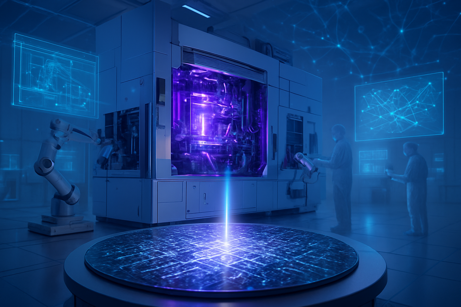
    At the heart of KLA's offerings are its defect inspection systems, including bright-field, multi-beam, and e-beam technologies. Unlike conventional methods, KLA's bright-field systems, such as the 2965 and 2950 EP, leverage enhanced broadband plasma illumination and advanced detection algorithms like Super•Pixel™ mode. These innovations allow for tunable illumination (from deep ultraviolet to visible light), significantly boosting contrast and sensitivity to detect yield-critical defects at ≤5nm logic and leading-edge memory design nodes. Furthermore, the revolutionary eSL10™ electron-beam patterned wafer defect inspection system employs a single, high-energy electron beam to uncover defects beyond the reach of traditional optical or even previous e-beam platforms. This unprecedented high-resolution, high-speed inspection is crucial for chips utilizing extreme ultraviolet (EUV) lithography, accelerating their time to market by identifying sub-optical yield-killing defects.

    KLA's metrology tools provide highly accurate measurements of critical dimensions, film layer thicknesses, layer-to-layer alignment, and surface topography. Systems like the SpectraFilm™ F1 for thin film measurement offer high precision for sub-7nm logic and leading-edge memory, providing early insights into electrical performance. The ATL100™ overlay metrology system, with its tunable laser technology, ensures 1nm resolution and real-time Homing™ capabilities for precise layer alignment even amidst production variations at ≤7nm nodes. These tools are critical for maintaining tight process control as semiconductor technology scales to atomic dimensions, where managing yield and critical dimensions becomes exceedingly complex.

    Moreover, KLA's in-situ process monitoring solutions, such as the SensArray® products, represent a significant departure from less frequent, offline monitoring. These systems utilize wired and wireless sensor wafers and reticles, coupled with automation and data analysis, to provide real-time monitoring of process tool environments and wafer handling conditions. Solutions like CryoTemp™ for dry etch processes and ScannerTemp™ for lithography scanners allow for immediate detection and correction of deviations, dramatically reducing chamber downtime and improving process stability.

    The industry's reaction to KLA's technological leadership has been overwhelmingly positive. KLA is consistently ranked among the top semiconductor equipment manufacturers, holding a dominant market share exceeding 50% in process control. Initial reactions from the AI research community and industry experts highlight KLA's aggressive integration of AI into its own tools. AI-driven algorithms enhance predictive maintenance, advanced defect detection and classification, yield management optimization, and sophisticated data analytics. This "AI-powered AI solutions" approach transforms raw production data into actionable insights, accelerating the production of the very integrated circuits (ICs) that power next-generation AI innovation. The establishment of KLA's AI and Modeling Center of Excellence in Ann Arbor, Michigan, further underscores its commitment to leveraging machine learning for advancements in semiconductor manufacturing.

    Enabling the Giants: KLA's Impact on the AI and Tech Landscape

    KLA Corporation's indispensable role in semiconductor manufacturing creates a profound ripple effect across the AI and tech industries, directly impacting tech giants, AI companies, and even influencing the viability of startups. Its technological leadership and market dominance position it as a critical enabler for the most advanced computing hardware.

    Major AI chip developers, including NVIDIA (NASDAQ: NVDA), Advanced Micro Devices (NASDAQ: AMD), and Intel (NASDAQ: INTC), are direct beneficiaries of KLA's advanced solutions. The ability to produce high-performance, high-yield AI accelerators—which are inherently complex and prone to microscopic defects—is fundamentally reliant on KLA's sophisticated process control tools. Without the precision and defect mitigation capabilities offered by KLA, manufacturing these powerful AI chips at scale would be significantly hampered, directly affecting the performance and cost efficiency of AI systems globally.

    Similarly, leading foundries like TSMC (NYSE: TSM) and Samsung (KRX: 005930) heavily depend on KLA's equipment. As these foundries push the boundaries with technologies like 2nm nodes and advanced packaging solutions such as CoWoS, KLA's tools become indispensable for managing the complexity of 3D stacking and chiplet integration. These advanced packaging techniques are crucial for next-generation AI and high-performance computing (HPC) chips. Furthermore, KLA benefits significantly from the growth in the DRAM market and investments in high-bandwidth memory (HBM), both of which are critical components for AI systems.

    KLA's dominant market position, however, creates high barriers to entry for startups and new entrants in semiconductor manufacturing or AI chip design. The highly specialized technical expertise, deep scientific understanding, and massive capital investment required for process control solutions make it challenging for new players to compete directly. Consequently, many smaller companies become reliant on established foundries that, in turn, are KLA's key customers. While KLA's market share in process control is formidable (over 50%), its role is largely complementary to other semiconductor equipment providers like Lam Research (NASDAQ: LRCX) (etch and deposition) and ASML (NASDAQ: ASML) (lithography), highlighting its indispensable partnership status within the ecosystem.

    The company's strategic advantages are numerous: an indispensable role at the epicenter of the AI-driven semiconductor cycle, high barriers to entry due to specialized technology, significant R&D investment (over 11% of revenue), and robust financial performance with industry-leading gross margins above 60%. KLA's "customer neutrality" within the industry—servicing virtually all major chip manufacturers—also provides a stable revenue stream, benefiting from the overall health and advancement of the semiconductor industry rather than the success of a single end-customer. This market positioning ensures KLA remains a pivotal force, driving the capabilities of AI and high-performance computing.

    The Unseen Backbone: KLA's Wider Significance in the AI Landscape

    KLA Corporation's wider significance extends far beyond its financial performance or market share; it acts as an often-unseen backbone, fundamentally enabling the broader AI landscape and driving critical semiconductor trends. Its contributions directly impact the overall progression of AI technology by ensuring the foundational hardware can meet increasingly stringent demands.

    By enabling the intricate and high-precision manufacturing of AI semiconductors, KLA facilitates the production of GPUs with leading-edge nodes, 3D transistor structures, large die sizes, and HBM. These advanced chips are the computational engines powering today's AI, and without KLA's ability to detect nanoscale defects and optimize production, their manufacture would be impossible. KLA's expertise in yield management and inspection is also crucial for advanced packaging techniques like 2.5D/3D stacking and chiplet architectures, which are becoming essential for creating high-performance, power-efficient AI systems through heterogeneous integration. The company's own integration of AI into its tools creates a powerful feedback loop: AI helps KLA build better chips, and these superior chips, in turn, enable smarter and more advanced AI systems.

    However, KLA's market dominance, with over 60% of the metrology and inspection segment, does raise some considerations. While indicative of strong competitive advantage and high barriers to entry, it positions KLA as a "gatekeeper" for advanced chip manufacturability. This concentration could potentially lead to concerns about pricing power or the lack of viable alternatives, although the highly specialized nature of the technology and continuous innovation mitigate some of these issues. The inherent complexity of KLA's technology, involving deep science, physics-based imaging, and sophisticated AI algorithms, also means that any significant disruption to its operations could have widespread implications for global semiconductor manufacturing. Furthermore, geopolitical risks, particularly U.S. export controls affecting its significant revenue from the Chinese market, and the cyclical nature of the semiconductor industry, present ongoing challenges.

    Comparing KLA's role to previous milestones highlights its enduring importance. While companies like ASML pioneered advanced lithography (the "printing press" for chips) and Applied Materials (NASDAQ: AMAT) developed key deposition and etching technologies, KLA's specialization in inspection and metrology acts as the "quality control engineer" for every step. Its evolution has paralleled Moore's Law, consistently providing the precision necessary as transistors shrank to atomic scales. Unlike direct AI milestones such as the invention of neural networks or large language models, KLA's significance lies in enabling the hardware foundation upon which these AI advancements are built. Its role is akin to the development of robust power grids and efficient computing architectures that underpinned early computational progress; without KLA, theoretical AI breakthroughs would remain largely academic. KLA ensures the quality and performance of the specialized hardware demanded by the current "AI supercycle," making it a pivotal enabler of the ongoing explosion in AI capabilities.

    The Road Ahead: Future Developments and Expert Outlook

    Looking to the future, KLA Corporation is strategically positioned for continued innovation and growth, driven by the relentless demands of the AI era and the ongoing miniaturization of semiconductors. Both its technological roadmap and market strategy are geared towards maintaining its indispensable role.

    In the near term, KLA is focused on enhancing its core offerings to support 2nm nodes and beyond, developing advanced metrology for critical dimensions and overlay measurements. Its defect inspection and metrology portfolio continues to expand with new systems for process development and control, leveraging AI-driven algorithms to accelerate data analysis and improve defect detection. Market-wise, KLA is aggressively capitalizing on the booming AI chip market and the rapid expansion of advanced packaging, anticipating outperforming the overall Wafer Fabrication Equipment (WFE) market growth in 2025 and projecting significant revenue increases from advanced packaging.

    Long-term, KLA's technological vision includes sustained investment in AI-driven algorithms for high-sensitivity inspection at optical speeds, and the development of solutions for quantum computing detection and extreme ultraviolet (EUV) lithography monitoring. Innovation in advanced packaging inspection remains a key focus, aligning with the industry's shift towards heterogeneous integration and 3D chip architectures. Strategically, KLA aims to sustain market leadership through increased process control intensity and market share gains, with its service business expected to grow significantly, targeting a 12-14% CAGR through 2026. The company also continues to evaluate strategic acquisitions and expand its global presence, as exemplified by its new R&D and manufacturing facility in Wales.

    However, KLA faces notable challenges. U.S. export controls on advanced semiconductor equipment to China pose a significant risk, impacting revenue from a historically major market. KLA is actively mitigating this through customer diversification and seeking export licenses. The inherent cyclicality of the semiconductor industry, competitive pressures from other equipment manufacturers, and potential supply chain disruptions remain constant considerations. Geopolitical risks and the evolving regulatory landscape further complicate market access and operations.

    Despite these challenges, experts and analysts are largely optimistic about KLA's future, particularly its role in the "AI supercycle." They view KLA as a "crucial enabler" and "hidden backbone" of the AI revolution, projecting a surge in demand for its advanced packaging and process control solutions by approximately 70% in 2025. KLA is expected to outperform the broader WFE market growth, with analysts forecasting a 7.5% CAGR through 2029. The increasing complexity of chips, moving towards 2nm and beyond, means KLA's process control tools will become even more essential for maintaining high yields and quality. Experts emphasize KLA's resilience in navigating market fluctuations and geopolitical headwinds, with its strategic focus on innovation and diversification expected to solidify its indispensable role in the evolving semiconductor landscape.

    The Indispensable Enabler: A Comprehensive Wrap-up

    KLA Corporation's position as a crucial equipment provider in the semiconductor ecosystem is not merely significant; it is foundational. The company's advanced process control and yield management solutions are the essential building blocks that enable the manufacturing of the world's most sophisticated chips, particularly those powering the burgeoning field of artificial intelligence. From nanoscale defect detection to precision metrology and real-time process monitoring, KLA ensures the quality, performance, and manufacturability of every silicon wafer, making it an indispensable partner for chip designers and foundries alike.

    This development underscores KLA's critical role as an enabler of technological progress. In an era defined by the rapid advancement of AI, KLA's technology allows for the creation of the high-performance processors and memory that fuel AI training and inference. Its own integration of AI into its tools further demonstrates a symbiotic relationship where AI helps refine the very process of creating advanced technology. KLA's market dominance, while posing some inherent considerations, reflects the immense technical barriers to entry and the specialized expertise required in this niche yet vital segment of the semiconductor industry.

    Looking ahead, KLA is poised for continued growth, driven by the insatiable demand for AI chips and the ongoing evolution of advanced packaging. Its strategic investments in R&D, coupled with its ability to adapt to complex geopolitical landscapes, will be key to its sustained leadership. What to watch for in the coming weeks and months includes KLA's ongoing innovation in 2nm node support, its expansion in advanced packaging solutions, and how it continues to navigate global trade dynamics. Ultimately, KLA's story is one of silent yet profound impact, cementing its legacy as a pivotal force in the history of technology and an unseen architect of the AI revolution.


    This content is intended for informational purposes only and represents analysis of current AI developments.

    TokenRing AI delivers enterprise-grade solutions for multi-agent AI workflow orchestration, AI-powered development tools, and seamless remote collaboration platforms.
    For more information, visit https://www.tokenring.ai/.

  • China Unleashes $70 Billion Semiconductor Gambit, Igniting New Front in Global Tech War

    China Unleashes $70 Billion Semiconductor Gambit, Igniting New Front in Global Tech War

    Beijing, China – December 12, 2025 – China is poised to inject an unprecedented $70 billion into its domestic semiconductor industry, a monumental financial commitment that signals an aggressive escalation in its quest for technological self-sufficiency. This colossal investment, potentially the largest governmental expenditure on chip manufacturing globally, is a direct and forceful response to persistent U.S. export controls and the intensifying geopolitical struggle for dominance in the critical tech sector. The move is set to reshape global supply chains, accelerate domestic innovation, and deepen the chasm of technological rivalry between the world's two largest economies.

    This ambitious push, which could see an additional 200 billion to 500 billion yuan (approximately $28 billion to $70 billion) channeled into the sector, builds upon a decade of substantial state-backed funding, including the recently launched $50 billion "Big Fund III" in late 2025. With an estimated $150 billion already invested since 2014, China's "whole-nation" approach, championed by President Xi Jinping, aims to decouple its vital technology industries from foreign reliance. The immediate significance lies in China's unwavering determination to reduce its dependence on external chip suppliers, particularly American giants, with early indicators already showing increased domestic chip output and declining import values for certain categories. This strategic pivot is not merely about economic growth; it is a calculated maneuver for national security and strategic autonomy in an increasingly fragmented global technological landscape.

    The Technical Crucible: Forging Self-Sufficiency in Silicon

    China's $70 billion semiconductor initiative is not a scattershot investment but a highly targeted and technically intricate strategy designed to bolster every facet of its domestic chip ecosystem. The core of this push involves a multi-pronged approach focusing on advanced manufacturing, materials, equipment, and crucially, the development of indigenous design capabilities, especially for critical AI chips.

    Technically, the investment aims to address long-standing vulnerabilities in China's semiconductor value chain. A significant portion of the funds is earmarked for advancing foundry capabilities, particularly in mature node processes (28nm and above) where China has seen considerable progress, but also pushing towards more advanced nodes (e.g., 7nm and 5nm) despite significant challenges imposed by export controls. Companies like Semiconductor Manufacturing International Corporation (SMIC) (SHA: 688981, HKG: 0981) are central to this effort, striving to overcome technological hurdles in lithography, etching, and deposition. The strategy also heavily emphasizes memory chip production, with companies like Yangtze Memory Technologies Co., Ltd. (YMTC) receiving substantial backing to compete in the NAND flash market.

    This current push differs from previous approaches by its sheer scale and increased focus on "hard tech" localization. Earlier investments often involved technology transfers or joint ventures; however, the stringent U.S. export controls have forced China to prioritize entirely indigenous research and development. This includes developing domestic alternatives for Electronic Design Automation (EDA) tools, critical chip manufacturing equipment (like steppers and scanners), and specialized materials. For instance, the focus on AI chips is paramount, with companies like Huawei HiSilicon and Cambricon Technologies (SHA: 688256) at the forefront of designing high-performance AI accelerators that can rival offerings from Nvidia (NASDAQ: NVDA). Initial reactions from the global AI research community acknowledge China's rapid progress in specific areas, particularly in AI chip design and mature node manufacturing, but also highlight the immense difficulty in replicating the entire advanced semiconductor ecosystem without access to cutting-edge Western technology. Experts are closely watching the effectiveness of China's "chiplet" strategies and heterogeneous integration techniques as workarounds to traditional monolithic advanced chip manufacturing.

    Corporate Impact: A Shifting Landscape of Winners and Challengers

    China's colossal semiconductor investment is poised to dramatically reshape the competitive landscape for both domestic and international technology companies, creating new opportunities for some while posing significant challenges for others. The primary beneficiaries within China will undoubtedly be the national champions that are strategically aligned with Beijing's self-sufficiency goals.

    Companies like SMIC (SHA: 688981, HKG: 0981), China's largest contract chipmaker, are set to receive substantial capital injections to expand their fabrication capacities and accelerate R&D into more advanced process technologies. This will enable them to capture a larger share of the domestic market, particularly for mature node chips critical for automotive, consumer electronics, and industrial applications. Huawei Technologies Co., Ltd., through its HiSilicon design arm, will also be a major beneficiary, leveraging the increased domestic foundry capacity and funding to further develop its Kunpeng and Ascend series processors, crucial for servers, cloud computing, and AI applications. Memory manufacturers like Yangtze Memory Technologies Co., Ltd. (YMTC) and Changxin Memory Technologies (CXMT) will see accelerated growth, aiming to reduce China's reliance on foreign DRAM and NAND suppliers. Furthermore, domestic equipment manufacturers, EDA tool developers, and material suppliers, though smaller, are critical to the "whole-nation" approach and will see unprecedented support to close the technology gap with international leaders.

    For international tech giants, particularly U.S. companies, the implications are mixed. While some may face reduced market access in China due to increased domestic competition and localization efforts, others might find opportunities in supplying less restricted components or collaborating on non-sensitive technologies. Companies like Nvidia (NASDAQ: NVDA) and Intel (NASDAQ: INTC), which have historically dominated the high-end chip market, will face intensified competition from Chinese alternatives, especially in the AI accelerator space. However, their established technological leads and global market penetration still provide significant advantages. European and Japanese equipment manufacturers might find themselves in a precarious position, balancing lucrative Chinese market access with pressure from U.S. export controls. The investment could disrupt existing supply chains, potentially leading to overcapacity in mature nodes globally and creating price pressures. Ultimately, the market positioning will be defined by a company's ability to innovate, adapt to geopolitical realities, and navigate a bifurcating global technology ecosystem.

    Broader Significance: A New Era of Techno-Nationalism

    China's $70 billion semiconductor push is far more than an economic investment; it is a profound declaration of techno-nationalism that will reverberate across the global AI landscape and significantly alter international relations. This initiative is a cornerstone of Beijing's broader strategy to achieve technological sovereignty, fundamentally reshaping the global technology order and intensifying the US-China tech rivalry.

    This aggressive move fits squarely into a global trend of nations prioritizing domestic semiconductor production, driven by lessons learned from supply chain disruptions and the strategic importance of chips for national security and economic competitiveness. It mirrors, and in some aspects surpasses, efforts like the U.S. CHIPS Act and similar initiatives in Europe and other Asian countries. However, China's scale and centralized approach are distinct. The impact on the global AI landscape is particularly significant: a self-sufficient China in semiconductors could accelerate its AI advancements without external dependencies, potentially leading to divergent AI ecosystems with different standards, ethical frameworks, and technological trajectories. This could foster greater innovation within China but also create compatibility challenges and deepen the ideological divide in technology.

    Potential concerns arising from this push include the risk of global overcapacity in certain chip segments, leading to price wars and reduced profitability for international players. There are also geopolitical anxieties about the dual-use nature of advanced semiconductors, with military applications of AI and high-performance computing becoming increasingly sophisticated. Comparisons to previous AI milestones, such as the initial breakthroughs in deep learning or the rise of large language models, highlight that while those were primarily technological advancements, China's semiconductor push is a foundational strategic move designed to enable all future technological advancements. It's not just about building a better AI model, but about building the entire infrastructure upon which any AI model can run, independent of foreign control. The stakes are immense, as the nation that controls the production of advanced chips ultimately holds a significant lever over future technological progress.

    The Road Ahead: Forecasts and Formidable Challenges

    The trajectory of China's $70 billion semiconductor push is poised to bring about significant near-term and long-term developments, though not without formidable challenges that experts are closely monitoring. In the near term, expect to see an accelerated expansion of mature node manufacturing capacity within China, which will further reduce reliance on foreign suppliers for chips used in consumer electronics, automotive, and industrial applications. This will likely lead to increased market share for domestic foundries and a surge in demand for locally produced equipment and materials. We can also anticipate more sophisticated indigenous designs for AI accelerators and specialized processors, with Chinese tech giants pushing the boundaries of what can be achieved with existing or slightly older process technologies through innovative architectural designs and packaging solutions.

    Longer-term, the ambition is to gradually close the gap in advanced process technologies, although this remains the most significant hurdle due to ongoing export controls on cutting-edge lithography equipment from companies like ASML Holding N.V. (AMS: ASML). Potential applications and use cases on the horizon include fully integrated domestic supply chains for critical infrastructure, advanced AI systems for smart cities and autonomous vehicles, and robust computing platforms for military and aerospace applications. Experts predict that while achieving full parity with the likes of Taiwan Semiconductor Manufacturing Company (TSMC) (NYSE: TSM) and Samsung (KRX: 005930) in leading-edge nodes will be an uphill battle, China will likely achieve a high degree of self-sufficiency in a broad range of critical, though not always bleeding-edge, semiconductor technologies.

    However, several challenges need to be addressed. Beyond the technological hurdles of advanced manufacturing, China faces a talent gap in highly specialized areas, despite massive investments in education and R&D. The economic viability of producing all chips domestically, potentially at higher costs, is another consideration. Geopolitically, the push could further entrench the "decoupling" trend, leading to a bifurcated global tech ecosystem with differing standards and potentially reduced interoperability. What experts predict will happen next is a continued, intense focus on incremental gains in process technology, aggressive investment in alternative manufacturing techniques like chiplets, and a relentless pursuit of breakthroughs in materials science and equipment development. The coming years will be a true test of China's ability to innovate under duress and forge an independent path in the most critical industry of the 21st century.

    Concluding Thoughts: A Defining Moment in AI and Global Tech

    China's $70 billion semiconductor initiative represents a pivotal moment in the history of artificial intelligence and global technology. It is a clear and decisive statement of intent, underscoring Beijing's unwavering commitment to technological sovereignty in the face of escalating international pressures. The key takeaway is that China is not merely reacting to restrictions but proactively building a parallel, self-sufficient ecosystem designed to insulate its strategic industries from external vulnerabilities.

    The significance of this development in AI history cannot be overstated. Access to advanced semiconductors is the bedrock of modern AI, from training large language models to deploying complex inference systems. By securing its chip supply, China aims to ensure an uninterrupted trajectory for its AI ambitions, potentially creating a distinct and powerful AI ecosystem. This move marks a fundamental shift from a globally integrated semiconductor industry to one increasingly fragmented along geopolitical lines. The long-term impact will likely include a more resilient but potentially less efficient global supply chain, intensified technological competition, and a deepening of the US-China rivalry that extends far beyond trade into the very architecture of future technology.

    In the coming weeks and months, observers should watch for concrete announcements regarding the allocation of the $70 billion fund, the specific companies receiving the largest investments, and any technical breakthroughs reported by Chinese foundries and design houses. The success or struggle of this monumental undertaking will not only determine China's technological future but also profoundly influence the direction of global innovation, economic power, and geopolitical stability for decades to come.


    This content is intended for informational purposes only and represents analysis of current AI developments.

    TokenRing AI delivers enterprise-grade solutions for multi-agent AI workflow orchestration, AI-powered development tools, and seamless remote collaboration platforms.
    For more information, visit https://www.tokenring.ai/.

  • Unlocking AI’s Full Potential: ASML’s EUV Lithography Becomes the Indispensable Foundation for Next-Gen Chips

    Unlocking AI’s Full Potential: ASML’s EUV Lithography Becomes the Indispensable Foundation for Next-Gen Chips

    The exponential growth of Artificial Intelligence (AI) and its insatiable demand for processing power have rendered traditional chip manufacturing methods inadequate, thrusting ASML's (AMS: ASML) Extreme Ultraviolet (EUV) lithography technology into an immediately critical and indispensable role. This groundbreaking technology, in which ASML holds a global monopoly, uses ultra-short 13.5-nanometer wavelengths of light to etch incredibly intricate patterns onto silicon wafers, enabling the creation of microchips with billions of smaller, more densely packed transistors.

    This unparalleled precision is the bedrock upon which next-generation AI accelerators, data center GPUs, and sophisticated edge AI solutions are built, providing the enhanced processing capabilities and vital energy efficiency required to power the most advanced AI applications today and in the immediate future. Without ASML's EUV systems, the semiconductor industry would face a significant barrier to scaling chip performance, making the continued advancement and real-world deployment of cutting-edge AI heavily reliant on this singular technological marvel.

    The Microscopic Marvel: Technical Deep Dive into EUV's Edge

    ASML's Extreme Ultraviolet (EUV) lithography technology represents a monumental leap in semiconductor manufacturing, enabling the creation of microchips with unprecedented density and performance. This intricate process is crucial for sustaining Moore's Law and powering the latest advancements in artificial intelligence (AI), high-performance computing, and other cutting-edge technologies. ASML is currently the sole supplier of EUV lithography systems globally.

    At the core of ASML's EUV technology is the use of light with an extremely short wavelength of 13.5 nanometers (nm), which is nearly in the X-ray range and more than 14 times shorter than the 193 nm wavelength used in previous Deep Ultraviolet (DUV) systems. This ultra-short wavelength is fundamental to achieving finer resolution and printing smaller features on silicon wafers. Key technical specifications include EUV light generated by firing two separate CO2 laser pulses at microscopic droplets of molten tin 50,000 times per second. Unlike DUV systems that use refractive lenses, EUV light is absorbed by nearly all materials, necessitating operation in a vacuum chamber and the use of highly specialized multi-layer mirrors, developed in collaboration with companies like Carl Zeiss SMT, to guide and focus the light. These mirrors are so precise that if scaled to the size of a country, the largest imperfection would be only about 1 millimeter.

    Current generation NXE systems (e.g., NXE:3400C, NXE:3600D) have a numerical aperture of 0.33, enabling them to print features with a resolution of 13 nm, supporting volume production for 7 nm, 5 nm, and 3 nm logic nodes. The next-generation platform, High-NA EUV (EXE platform, e.g., TWINSCAN EXE:5000, EXE:5200B), significantly increases the numerical aperture to 0.55, improving resolution to just 8 nm. This allows for transistors that are 1.7 times smaller and transistor densities 2.9 times higher. The first High-NA EUV system was delivered in December 2023, with high-volume manufacturing expected between 2025 and 2026 for advanced nodes starting at 2 nm logic. High-NA EUV systems are designed for higher productivity, with initial capabilities of printing over 185 wafers per hour (wph).

    The transition from Deep Ultraviolet (DUV) to Extreme Ultraviolet (EUV) lithography marks a fundamental shift. The most significant difference is the light wavelength—13.5 nm for EUV compared to 193 nm for DUV. DUV systems use refractive lenses and can operate in air, while EUV necessitates an entirely reflective optical system within a vacuum. EUV can achieve much smaller feature sizes, enabling advanced nodes where DUV lithography typically hits its limit around 40-20 nm without complex resolution enhancement techniques like multi-patterning, which EUV often simplifies into a single pass. The AI research community and industry experts have expressed overwhelmingly positive reactions, recognizing EUV's indispensable role in sustaining Moore's Law and enabling the fabrication of the ever-smaller, more powerful, and energy-efficient chips required for the exponential growth in AI, quantum computing, and other advanced technologies.

    Reshaping the AI Battleground: Corporate Beneficiaries and Competitive Edge

    ASML's EUV lithography technology is a pivotal enabler for the advancement of artificial intelligence, profoundly impacting AI companies, tech giants, and startups by shaping the capabilities, costs, and competitive landscape of advanced chip manufacturing. It is critical for producing the advanced semiconductors that power AI systems, allowing for higher transistor densities, increased processing capabilities, and lower power consumption in AI chips. This is essential for scaling semiconductor devices to 7nm, 5nm, 3nm, and even sub-2nm nodes, which are vital for developing specialized AI accelerators and neural processing units.

    The companies that design and manufacture the most advanced AI chips are the primary beneficiaries of ASML's EUV technology. TSMC (NYSE: TSM), as the world's largest contract chipmaker, is a leading implementer of EUV, extensively integrating it into its fabrication processes for nodes such as N7+, N5, N3, and the upcoming N2. TSMC received its first High-NA (High Numerical Aperture) EUV machine in September 2024, signaling its commitment to maintaining leadership in advanced AI chip manufacturing, with plans to integrate it into its A14 (1.4nm) process node by 2027. Samsung Electronics (KRX: 005930) is another key player heavily investing in EUV, planning to deploy High-NA EUV at its 2nm node, potentially ahead of TSMC's 1.4nm timeline, with a significant investment in two of ASML’s EXE:5200B High-NA EUV tools. Intel (NASDAQ: INTC) is actively adopting ASML's EUV and High-NA EUV machines as part of its strategy to regain leadership in chip manufacturing, particularly for AI, with its roadmap including High-NA EUV for its Intel 18A process, with product proof points in 2025. Fabless giants like NVIDIA (NASDAQ: NVDA) and AMD (NASDAQ: AMD) rely entirely on these advanced foundries. ASML's EUV technology is indispensable for producing the highly complex and dense chips that power NVIDIA's AI accelerators, such as the Blackwell architecture and the upcoming 'Rubin' platform, and AMD's high-performance CPUs and GPUs for AI workloads.

    ASML's EUV technology creates a clear divide in the competitive landscape. Tech giants and major AI labs that partner with or own foundries capable of leveraging EUV gain a significant strategic advantage, accessing the most advanced, powerful, and energy-efficient chips crucial for developing and deploying cutting-edge AI models. Conversely, companies without access to EUV-fabricated chips face substantial hurdles, as the computational demands of advanced AI would become "prohibitively expensive or technically unfeasible." ASML's near-monopoly makes it an indispensable "linchpin" and "gatekeeper" of the AI revolution, granting it significant pricing power and strategic importance. The immense capital expenditure (EUV machines cost hundreds of millions of dollars) and the complexity of integrating EUV technology create high barriers to entry for new players and smaller startups in advanced chip manufacturing, concentrating leading-edge AI chip production among a few well-established tech giants.

    The Unseen Engine: Broader Implications for AI and Beyond

    ASML's Extreme Ultraviolet (EUV) lithography technology stands as a pivotal advancement in semiconductor manufacturing, profoundly shaping the landscape of artificial intelligence (AI). By enabling the creation of smaller, more powerful, and energy-efficient chips, EUV is not merely an incremental improvement but a foundational technology indispensable for the continued progression of AI capabilities.

    The relentless demand for computational power in AI, driven by the increasing complexity of algorithms and the processing of vast datasets, necessitates increasingly sophisticated semiconductor hardware. EUV lithography, operating at an ultra-short wavelength of 13.5 nanometers, allows manufacturers to etch incredibly fine features onto silicon wafers, crucial for producing advanced semiconductor nodes like 7nm, 5nm, 3nm, and the forthcoming sub-2nm generations that power cutting-edge AI processors. Without EUV, the semiconductor industry would face significant challenges in meeting the escalating hardware demands of AI, potentially slowing the pace of innovation.

    EUV lithography has been instrumental in extending the viability of Moore's Law, providing the necessary foundation for continued miniaturization and performance enhancement beyond the limits of traditional methods. By enabling the packing of billions of tiny transistors, EUV contributes to significant improvements in power efficiency. This allows AI chips to process more parameters with lower power requirements per computation, reducing the overall energy consumption of AI systems at scale—a crucial benefit as AI applications demand massive computational power. The higher transistor density and performance directly translate into more powerful and capable AI systems, essential for complex AI algorithms, training large language models, and real-time inference at the edge, fostering breakthroughs in areas such as autonomous driving, medical diagnostics, and augmented reality.

    Despite its critical role, ASML's EUV technology faces several significant concerns. Each EUV system is incredibly expensive, costing between $150 million and $400 million, with the latest High-NA models exceeding $370 million, limiting accessibility to a handful of leading chip manufacturers. The machines are marvels of engineering but are immensely complex, comprising over 100,000 parts and requiring operation in a vacuum, leading to high installation, maintenance, and operational costs. ASML's near-monopoly places it at the center of global geopolitical tensions, particularly between the United States and China, with export controls highlighting its strategic importance and impacting sales. This concentration in the supply chain also creates a significant risk, as disruptions can impact advanced chip production schedules globally.

    The impact of ASML's EUV lithography on AI is analogous to several foundational breakthroughs that propelled computing and, subsequently, AI forward. Just as the invention of the transistor revolutionized electronics, EUV pushes the physical limits of transistor density. Similarly, its role in enabling the creation of advanced chips that house powerful GPUs for parallel processing mirrors the significance of the GPU's development for AI. While EUV is not an AI algorithm or a software breakthrough, it is a crucial hardware innovation that unlocks the potential for these software advancements, effectively serving as the "unseen engine" behind the AI revolution.

    The Road Ahead: Future Horizons for EUV and AI

    ASML's Extreme Ultraviolet (EUV) lithography technology is a cornerstone of advanced semiconductor manufacturing, indispensable for producing the high-performance chips that power artificial intelligence (AI) applications. The company is actively pursuing both near-term and long-term developments to push the boundaries of chip scaling, while navigating significant technical and geopolitical challenges.

    ASML's immediate focus is on the rollout of its next-generation High-NA EUV lithography systems, specifically the TWINSCAN EXE:5000 and EXE:5200 platforms. These High-NA systems increase the numerical aperture from 0.33 to 0.55, allowing for a critical dimension (CD) of 8 nm, enabling chipmakers to print transistors 1.7 times smaller and achieve transistor densities 2.9 times higher. The first modules of the EXE:5000 were shipped to Intel (NASDAQ: INTC) in December 2023 for R&D, with high-volume manufacturing using High-NA EUV anticipated to begin in 2025-2026. High-NA EUV is crucial for enabling the production of sub-2nm logic nodes, including 1.5nm and 1.4nm. Beyond High-NA, ASML is in early R&D for "Hyper-NA" EUV technology, envisioned with an even higher numerical aperture of 0.75, expected to be deployed around 2030-2035 to push transistor densities beyond the projected limits of High-NA.

    ASML's advanced EUV lithography is fundamental to the progression of AI hardware, enabling the manufacturing of high-performance AI chips, neural processors, and specialized AI accelerators that demand massive computational power and energy efficiency. By enabling smaller, more densely packed transistors, EUV facilitates increased processing capabilities and lower power consumption, critical for AI hardware across diverse applications, including data centers, edge AI in smartphones, and autonomous systems. High-NA EUV will also support advanced packaging technologies, such as chiplets and 3D stacking, increasingly important for managing the complexity of AI chips and facilitating real-time AI processing at the edge.

    Despite its critical role, EUV technology faces several significant challenges. The high cost of High-NA machines (between €350 million and $380 million per unit) can hinder widespread adoption. Technical complexities include inefficient light sources, defectivity issues (like pellicle readiness), challenges with resist materials at small feature sizes, and the difficulty of achieving sub-2nm overlay accuracy. Supply chain and geopolitical risks, such as ASML's monopoly and export restrictions, also pose significant hurdles. Industry experts and ASML itself are highly optimistic, forecasting significant growth driven by the surging demand for advanced AI chips. High-NA EUV is widely regarded as the "only path to next-generation chips" and an "indispensable" technology for producing powerful processors for data centers and AI, with predictions of ASML achieving a trillion-dollar valuation by 2034-2036.

    The Unseen Architect of AI's Future: A Concluding Perspective

    ASML's Extreme Ultraviolet (EUV) lithography technology stands as a critical enabler in the ongoing revolution of Artificial Intelligence (AI) chips, underpinning advancements that drive both the performance and efficiency of modern computing. The Dutch company (AMS: ASML) holds a near-monopoly in the production of these highly sophisticated machines, making it an indispensable player in the global semiconductor industry.

    Key takeaways highlight EUV's vitality for manufacturing the most advanced AI chips, enabling intricate patterns at scales of 5 nanometers and below, extending to 3nm and even sub-2nm with next-generation High-NA EUV systems. This precision allows for significantly higher transistor density, directly translating to increased processing capabilities and improved energy efficiency—both critical for powerful AI applications. Leading chip manufacturers like Taiwan Semiconductor Manufacturing Co. (NYSE: TSM), Samsung (KRX: 005930), and Intel (NASDAQ: INTC) rely on ASML's EUV machines to produce cutting-edge chips that power everything from NVIDIA's (NASDAQ: NVDA) AI accelerators to Apple's (NASDAQ: AAPL) smartphones. ASML's dominant market position, coupled with robust demand for AI chips, is a significant driver for its projected growth, with the company forecasting annual revenues between €44 billion and €60 billion by 2030.

    The development and widespread adoption of ASML's EUV lithography mark a pivotal moment in AI history. Without this technology, the production of next-generation AI chipsets capable of meeting the ever-growing demands of AI applications would be challenging, potentially stalling the rapid progress seen in the field. EUV is a cornerstone for the future of AI, enabling the complex designs and high transistor densities required for sophisticated AI algorithms, large language models, and real-time processing in areas like self-driving cars, medical diagnostics, and edge AI. It is not merely an advancement but an essential foundation upon which the future of AI and computing is being built.

    The long-term impact of ASML's EUV technology on AI is profound and enduring. By enabling the continuous scaling of semiconductors, ASML ensures that the hardware infrastructure can keep pace with the rapidly evolving demands of AI software and algorithms. This technological imperative extends beyond AI, influencing advancements in 5G, the Internet of Things (IoT), and quantum computing. ASML's role solidifies its position as a "tollbooth" for the AI highway, as it provides the fundamental tools that every advanced chipmaker needs. This unique competitive moat, reinforced by continuous innovation like High-NA EUV, suggests that ASML will remain a central force in shaping the technological landscape for decades to come, ensuring the continued evolution of AI-driven innovations.

    In the coming weeks and months, several key areas will be crucial to monitor. Watch for the successful deployment and performance validation of ASML's next-generation High-NA EUV machines, which are essential for producing sub-2nm chips. The ongoing impact of geopolitical landscape and export controls on ASML's sales to China will also be a significant factor. Furthermore, keep an eye on ASML's order bookings and revenue reports for insights into the balance between robust AI-driven demand and potential slowdowns in other chip markets, as well as any emerging competition or alternative miniaturization technologies, though no immediate threats to ASML's EUV dominance exist. Finally, ASML's progress towards its ambitious gross margin targets of 56-60% by 2030 will indicate the efficiency gains from High-NA EUV and overall cost control. By closely monitoring these developments, observers can gain a clearer understanding of the evolving synergy between ASML's groundbreaking lithography technology and the accelerating advancements in AI.


    This content is intended for informational purposes only and represents analysis of current AI developments.

    TokenRing AI delivers enterprise-grade solutions for multi-agent AI workflow orchestration, AI-powered development tools, and seamless remote collaboration platforms.
    For more information, visit https://www.tokenring.ai/.
  • Broadcom’s AI Surge: Record Q4 Earnings Fuel Volatility in Semiconductor Market

    Broadcom’s AI Surge: Record Q4 Earnings Fuel Volatility in Semiconductor Market

    Broadcom's (NASDAQ: AVGO) recent Q4 fiscal year 2025 earnings report, released on December 11, 2025, sent ripples through the technology sector, showcasing a remarkable surge in its artificial intelligence (AI) semiconductor business. While the company reported robust financial performance, with total revenue hitting approximately $18.02 billion—a 28% year-over-year increase—and AI semiconductor revenue skyrocketing by 74%, the immediate market reaction was a mix of initial enthusiasm followed by notable volatility. This report underscores Broadcom's pivotal and growing role in powering the global AI infrastructure, yet also highlights investor sensitivity to future guidance and market dynamics.

    The impressive figures reveal Broadcom's strategic success in capitalizing on the insatiable demand for custom AI chips and data center solutions. With AI semiconductor revenue reaching $8.2 billion in Q4 FY2025 and an overall AI revenue of $20 billion for the fiscal year, the company's trajectory in the AI domain is undeniable. However, the subsequent dip in stock price, despite the strong numbers, suggests that investors are closely scrutinizing factors like the reported $73 billion AI product backlog, projected profit margin shifts, and broader market sentiment, signaling a complex interplay of growth and cautious optimism in the high-stakes AI semiconductor arena.

    Broadcom's AI Engine: Custom Chips and Rack Systems Drive Innovation

    Broadcom's Q4 2025 earnings report illuminated the company's deepening technical prowess in the AI domain, driven by its custom AI accelerators, known as XPUs, and its integral role in Google's (NASDAQ: GOOGL) latest-generation Ironwood TPU rack systems. These advancements underscore a strategic pivot towards highly specialized, integrated solutions designed to power the most demanding AI workloads at hyperscale.

    At the heart of Broadcom's AI strategy are its custom XPUs, Application-Specific Integrated Circuits (ASICs) co-developed with major hyperscale clients such as Google, Meta Platforms (NASDAQ: META), ByteDance, and OpenAI. These chips are engineered for unparalleled performance per watt and cost efficiency, tailored precisely for specific AI algorithms. Technical highlights include next-generation 2-nanometer (2nm) AI XPUs, capable of an astonishing 10,000 trillion calculations per second (10,000 Teraflops). A significant innovation is the 3.5D eXtreme Dimension System in Package (XDSiP) platform, launched in December 2024. This advanced packaging technology integrates over 6000 mm² of silicon and up to 12 High Bandwidth Memory (HBM) modules, leveraging TSMC's (NYSE: TSM) cutting-edge process nodes and 2.5D CoWoS packaging. Its proprietary 3.5D Face-to-Face (F2F) technology dramatically enhances signal density and reduces power consumption in die-to-die interfaces, with initial products expected in production shipments by February 2026. Complementing these chips are Broadcom's high-speed networking switches, like the Tomahawk and Jericho lines, essential for building massive AI clusters capable of connecting up to a million XPUs.

    Broadcom's decade-long partnership with Google in developing Tensor Processing Units (TPUs) culminated in the Ironwood (TPU v7) rack systems, a cornerstone of its Q4 success. Ironwood is specifically designed for the "most demanding workloads," including large-scale model training, complex reinforcement learning, and high-volume AI inference. It boasts a 10x peak performance improvement over TPU v5p and more than 4x better performance per chip for both training and inference compared to TPU v6e (Trillium). Each Ironwood chip delivers 4,614 TFLOPS of processing power with 192 GB of memory and 7.2 TB/s bandwidth, while offering 2x the performance per watt of the Trillium generation. These TPUs are designed for immense scalability, forming "pods" of 256 chips and "Superpods" of 9,216 chips, capable of achieving 42.5 exaflops of performance—reportedly 24 times more powerful than the world's largest supercomputer, El Capitan. Broadcom is set to deploy these 64-TPU-per-rack systems for customers like OpenAI, with rollouts extending through 2029.

    This approach significantly differs from the general-purpose GPU strategy championed by competitors like Nvidia (NASDAQ: NVDA). While Nvidia's GPUs offer versatility and a robust software ecosystem, Broadcom's custom ASICs prioritize superior performance per watt and cost efficiency for targeted AI workloads. Broadcom is transitioning into a system-level solution provider, offering integrated infrastructure encompassing compute, memory, and high-performance networking, akin to Nvidia's DGX and HGX solutions. Its co-design partnership model with hyperscalers allows clients to optimize for cost, performance, and supply chain control, driving a "build over buy" trend in the industry. Initial reactions from the AI research community and industry experts have validated Broadcom's strategy, recognizing it as a "silent winner" in the AI boom and a significant challenger to Nvidia's market dominance, with some reports even suggesting Nvidia is responding by establishing a new ASIC department.

    Broadcom's AI Dominance: Reshaping the Competitive Landscape

    Broadcom's AI-driven growth and custom XPU strategy are fundamentally reshaping the competitive dynamics within the AI semiconductor market, creating clear beneficiaries while intensifying competition for established players like Nvidia. Hyperscale cloud providers and leading AI labs stand to gain the most from Broadcom's specialized offerings. Companies like Google (NASDAQ: GOOGL), Meta Platforms (NASDAQ: META), OpenAI, Anthropic, ByteDance, Microsoft (NASDAQ: MSFT), and Amazon (NASDAQ: AMZN) are primary beneficiaries, leveraging Broadcom's custom AI accelerators and networking solutions to optimize their vast AI infrastructures. Broadcom's deep involvement in Google's TPU development and significant collaborations with OpenAI and Anthropic for custom silicon and Ethernet solutions underscore its indispensable role in their AI strategies.

    The competitive implications for major AI labs and tech companies are profound, particularly in relation to Nvidia (NASDAQ: NVDA). While Nvidia remains dominant with its general-purpose GPUs and CUDA ecosystem for AI training, Broadcom's focus on custom ASICs (XPUs) and high-margin networking for AI inference workloads presents a formidable alternative. This "build over buy" option for hyperscalers, enabled by Broadcom's co-design model, provides major tech companies with significant negotiating leverage and is expected to erode Nvidia's pricing power in certain segments. Analysts even project Broadcom to capture a significant share of total AI semiconductor revenue, positioning it as the second-largest player after Nvidia by 2026. This shift allows tech giants to diversify their supply chains, reduce reliance on a single vendor, and achieve superior performance per watt and cost efficiency for their specific AI models.

    This strategic shift is poised to disrupt several existing products and services. The rise of custom ASICs, optimized for inference, challenges the widespread reliance on general-purpose GPUs for all AI workloads, forcing a re-evaluation of hardware strategies across the industry. Furthermore, Broadcom's acquisition of VMware (NYSE: VMW) is positioning it to offer "Private AI" solutions, potentially disrupting the revenue streams of major public cloud providers by enabling enterprises to run AI workloads on their private infrastructure with enhanced security and control. However, this trend could also create higher barriers to entry for AI startups, who may struggle to compete with well-funded tech giants leveraging proprietary custom AI hardware.

    Broadcom is solidifying a formidable market position as a premier AI infrastructure supplier, controlling approximately 70% of the custom AI ASIC market and establishing its Tomahawk and Jericho platforms as de facto standards for hyperscale Ethernet switching. Its strategic advantages stem from its custom silicon expertise and co-design model, deep and concentrated relationships with hyperscalers, dominance in AI networking, and the synergistic integration of VMware's software capabilities. These factors make Broadcom an indispensable "plumbing" provider for the next wave of AI capacity, offering cost-efficiency for AI inference and reinforcing its strong financial performance and growth outlook in the rapidly evolving AI landscape.

    Broadcom's AI Trajectory: Broader Implications and Future Horizons

    Broadcom's success with custom XPUs and its strategic positioning in the AI semiconductor market are not isolated events; they are deeply intertwined with, and actively shaping, the broader AI landscape. This trend signifies a major shift towards highly specialized hardware, moving beyond the limitations of general-purpose CPUs and even GPUs for the most demanding AI workloads. As AI models grow exponentially in complexity and scale, the industry is witnessing a strategic pivot by tech giants to design their own in-house chips, seeking granular control over performance, energy efficiency, and supply chain security—a trend Broadcom is expertly enabling.

    The wider impacts of this shift are profound. In the semiconductor industry, Broadcom's ascent is intensifying competition, particularly challenging Nvidia's long-held dominance, and is likely to lead to a significant restructuring of the global AI chip supply chain. This demand for specialized AI silicon is also fueling unprecedented innovation in semiconductor design and manufacturing, with AI algorithms themselves being leveraged to automate and optimize chip production processes. For data center architecture, the adoption of custom XPUs is transforming traditional server farms into highly specialized, AI-optimized "supercenters." These modern data centers rely heavily on tightly integrated environments that combine custom accelerators with advanced networking solutions—an area where Broadcom's high-speed Ethernet chips, like the Tomahawk and Jericho series, are becoming indispensable for managing the immense data flow.

    Regarding the development of AI models, custom silicon provides the essential computational horsepower required for training and deploying sophisticated models with billions of parameters. By optimizing hardware for specific AI algorithms, these chips enable significant improvements in both performance and energy efficiency during model training and inference. This specialization facilitates real-time, low-latency inference for AI agents and supports the scalable deployment of generative AI across various platforms, ultimately empowering companies to undertake ambitious AI projects that would otherwise be cost-prohibitive or computationally intractable.

    However, this accelerated specialization comes with potential concerns and challenges. The development of custom hardware requires substantial upfront investment in R&D and talent, and Broadcom itself has noted that its rapidly expanding AI segment, particularly custom XPUs, typically carries lower gross margins. There's also the challenge of balancing specialization with the need for flexibility to adapt to the fast-paced evolution of AI models, alongside the critical need for a robust software ecosystem to support new custom hardware. Furthermore, heavy reliance on a few custom silicon suppliers could lead to vendor lock-in and concentration risks, while the sheer energy consumption of AI hardware necessitates continuous innovation in cooling systems. The massive scale of investment in AI infrastructure has also raised concerns about market volatility and potential "AI bubble" fears. Compared to previous AI milestones, such as the initial widespread adoption of GPUs for deep learning, the current trend signifies a maturation and diversification of the AI hardware landscape, where both general-purpose leaders and specialized custom silicon providers can thrive by meeting diverse and insatiable AI computing needs.

    The Road Ahead: Broadcom's AI Future and Industry Evolution

    Broadcom's trajectory in the AI sector is set for continued acceleration, driven by its strategic focus on custom AI accelerators, high-performance networking, and software integration. In the near term, the company projects its AI semiconductor revenue to double year-over-year in Q1 fiscal year 2026, reaching $8.2 billion, building on a 74% growth in the most recent quarter. This momentum is fueled by its leadership in custom ASICs, where it holds approximately 70% of the market, and its pivotal role in Google's Ironwood TPUs, backed by a substantial $73 billion AI backlog expected over the next 18 months. Broadcom's Ethernet-based networking portfolio, including Tomahawk switches and Jericho routers, will remain critical for hyperscalers building massive AI clusters. Long-term, Broadcom envisions its custom-silicon business exceeding $100 billion by the decade's end, aiming for a 24% share of the overall AI chip market by 2027, bolstered by its VMware acquisition to integrate AI into enterprise software and private/hybrid cloud solutions.

    The advancements spearheaded by Broadcom are enabling a vast array of AI applications and use cases. Custom AI accelerators are becoming the backbone for highly efficient AI inference and training workloads in hyperscale data centers, with major cloud providers leveraging Broadcom's custom silicon for their proprietary AI infrastructure. High-performance AI networking, facilitated by Broadcom's switches and routers, is crucial for preventing bottlenecks in these massive AI systems. Through VMware, Broadcom is also extending AI into enterprise infrastructure management, security, and cloud operations, enabling automated infrastructure management, standardized AI workloads on Kubernetes, and certified nodes for AI model training and inference. On the software front, Broadcom is applying AI to redefine software development with coding agents and intelligent automation, and integrating generative AI into Spring Boot applications for AI-driven decision-making.

    Despite this promising outlook, Broadcom and the wider industry face significant challenges. Broadcom itself has noted that the growing sales of lower-margin custom AI processors are impacting its overall profitability, with expected gross margin contraction. Intense competition from Nvidia and AMD, coupled with geopolitical and supply chain risks, necessitates continuous innovation and strategic diversification. The rapid pace of AI innovation demands sustained and significant R&D investment, and customer concentration risk remains a factor, as a substantial portion of Broadcom's AI revenue comes from a few hyperscale clients. Furthermore, broader "AI bubble" concerns and the massive capital expenditure required for AI infrastructure continue to scrutinize valuations across the tech sector.

    Experts predict an unprecedented "giga cycle" in the semiconductor industry, driven by AI demand, with the global semiconductor market potentially reaching the trillion-dollar threshold before the decade's end. Broadcom is widely recognized as a "clear ASIC winner" and a "silent winner" in this AI monetization supercycle, expected to remain a critical infrastructure provider for the generative AI era. The shift towards custom AI chips (ASICs) for AI inference tasks is particularly significant, with projections indicating 80% of inference tasks in 2030 will use ASICs. Given Broadcom's dominant market share in custom AI processors, it is exceptionally well-positioned to capitalize on this trend. While margin pressures and investment concerns exist, expert sentiment largely remains bullish on Broadcom's long-term prospects, highlighting its diversified business model, robust AI-driven growth, and strategic partnerships. The market is expected to see continued bifurcation into hyper-growth AI and stable non-AI segments, with consolidation and strategic partnerships becoming increasingly vital.

    Broadcom's AI Blueprint: A New Era of Specialized Computing

    Broadcom's Q4 fiscal year 2025 earnings report and its robust AI strategy mark a pivotal moment in the history of artificial intelligence, solidifying the company's role as an indispensable architect of the modern AI era. Key takeaways from the report include record total revenue of $18.02 billion, driven significantly by a 74% year-over-year surge in AI semiconductor revenue to $6.5 billion in Q4. Broadcom's strategy, centered on custom AI accelerators (XPUs), high-performance networking solutions, and strategic software integration via VMware, has yielded a substantial $73 billion AI product order backlog. This focus on open, scalable, and power-efficient technologies for AI clusters, despite a noted impact on overall gross margins due to the shift towards providing complete rack systems, positions Broadcom at the very heart of hyperscale AI infrastructure.

    This development holds immense significance in AI history, signaling a critical diversification of AI hardware beyond the traditional dominance of general-purpose GPUs. Broadcom's success with custom ASICs validates a growing trend among hyperscalers to opt for specialized chips tailored for optimal performance, power efficiency, and cost-effectiveness at scale, particularly for AI inference. Furthermore, Broadcom's leadership in high-bandwidth Ethernet switches and co-packaged optics underscores the paramount importance of robust networking infrastructure as AI models and clusters continue to grow exponentially. The company is not merely a chip provider but a foundational architect, enabling the "nervous system" of AI data centers and facilitating the crucial "inference phase" of AI development, where models are deployed for real-world applications.

    The long-term impact on the tech industry and society will be profound. Broadcom's strategy is poised to reshape the competitive landscape, fostering a more diverse AI hardware market that could accelerate innovation and drive down deployment costs. Its emphasis on power-efficient designs will be crucial in mitigating the environmental and economic impact of scaling AI infrastructure. By providing the foundational tools for major AI developers, Broadcom indirectly facilitates the development and widespread adoption of increasingly sophisticated AI applications across all sectors, from advanced cloud services to healthcare and finance. The trend towards integrated, "one-stop" solutions, as exemplified by Broadcom's rack systems, also suggests deeper, more collaborative partnerships between hardware providers and large enterprises.

    In the coming weeks and months, several key indicators will be crucial to watch. Investors will be closely monitoring Broadcom's ability to stabilize its gross margins as its AI revenue continues its aggressive growth trajectory. The timely fulfillment of its colossal $73 billion AI backlog, particularly deliveries to major customers like Anthropic and the newly announced fifth XPU customer, will be a testament to its execution capabilities. Any announcements of new large-scale partnerships or further diversification of its client base will reinforce its market position. Continued advancements and adoption of Broadcom's next-generation networking solutions, such as Tomahawk 6 and Co-packaged Optics, will be vital as AI clusters demand ever-increasing bandwidth. Finally, observing the broader competitive dynamics in the custom silicon market and how other companies respond to Broadcom's growing influence will offer insights into the future evolution of AI infrastructure. Broadcom's journey will serve as a bellwether for the evolving balance between specialized hardware, high-performance networking, and the economic realities of delivering comprehensive AI solutions.


    This content is intended for informational purposes only and represents analysis of current AI developments.

    TokenRing AI delivers enterprise-grade solutions for multi-agent AI workflow orchestration, AI-powered development tools, and seamless remote collaboration platforms.
    For more information, visit https://www.tokenring.ai/.

  • The AI-Driven Data Center Boom: Igniting a Domestic Semiconductor Manufacturing Revolution

    The AI-Driven Data Center Boom: Igniting a Domestic Semiconductor Manufacturing Revolution

    The global technology landscape is undergoing a profound transformation, with the relentless expansion of the data center industry, fueled primarily by the insatiable demands of artificial intelligence (AI) and machine learning (ML), creating an unprecedented surge in demand for advanced semiconductors. This critical synergy is not merely an economic phenomenon but a strategic imperative, driving nations worldwide to prioritize and heavily invest in domestic semiconductor manufacturing, aiming for self-sufficiency and robust supply chain resilience. As of late 2025, this interplay is reshaping industrial policies, fostering massive investments, and accelerating innovation at a scale unseen in decades.

    The exponential growth of cloud computing, digital transformation initiatives across all sectors, and the rapid deployment of generative AI applications are collectively propelling the data center market to new heights. Valued at approximately $215 billion in 2023, the market is projected to reach $450 billion by 2030, with some estimates suggesting it could nearly triple to $776 billion by 2034. This expansion, particularly in hyperscale data centers, which have seen their capacity double since 2020, necessitates a foundational shift in how critical components, especially advanced chips, are sourced and produced. The implications are clear: the future of AI and digital infrastructure hinges on a secure and robust supply of cutting-edge semiconductors, sparking a global race to onshore manufacturing capabilities.

    The Technical Core: AI's Insatiable Appetite for Advanced Silicon

    The current data center boom is fundamentally distinct from previous cycles due to the unique and demanding nature of AI workloads. Unlike traditional computing, AI, especially generative AI, requires immense computational power, high-speed data processing, and specialized memory solutions. This translates into an unprecedented demand for a specific class of advanced semiconductors:

    Graphics Processing Units (GPUs) and AI Application-Specific Integrated Circuits (ASICs): GPUs remain the cornerstone of AI infrastructure, with one leading manufacturer capturing an astounding 93% of the server GPU revenue in 2024. GPU revenue is forecasted to soar from $100 billion in 2024 to $215 billion by 2030. Concurrently, AI ASICs are rapidly gaining traction, particularly as hyperscalers like Alphabet (NASDAQ: GOOGL), Amazon (NASDAQ: AMZN), and Microsoft (NASDAQ: MSFT) develop custom silicon to optimize performance, reduce latency, and lessen their reliance on third-party manufacturers. Revenue from AI ASICs is expected to reach almost $85 billion by 2030, marking a significant shift towards proprietary hardware solutions.

    Advanced Memory Solutions: To handle the vast datasets and complex models of AI, High Bandwidth Memory (HBM) and Graphics Double Data Rate (GDDR) are crucial. HBM, in particular, is experiencing explosive growth, with revenue projected to surge by up to 70% in 2025, reaching an impressive $21 billion. These memory technologies are vital for providing the necessary throughput to keep AI accelerators fed with data.

    Networking Semiconductors: The sheer volume of data moving within and between AI-powered data centers necessitates highly advanced networking components. Ethernet switches, optical interconnects, SmartNICs, and Data Processing Units (DPUs) are all seeing accelerated development and deployment, with networking semiconductor growth projected at 13% in 2025 to overcome latency and throughput bottlenecks. Furthermore, Wide Bandgap (WBG) materials like Silicon Carbide (SiC) and Gallium Nitride (GaN) are increasingly being adopted in data center power supplies. These materials offer superior efficiency, operate at higher temperatures and voltages, and significantly reduce power loss, contributing to more energy-efficient and sustainable data center operations.

    The initial reaction from the AI research community and industry experts has been one of intense focus on hardware innovation. The limitations of current silicon architectures for increasingly complex AI models are pushing the boundaries of chip design, packaging technologies, and cooling solutions. This drive for specialized, high-performance, and energy-efficient hardware represents a significant departure from the more generalized computing needs of the past, signaling a new era of hardware-software co-design tailored specifically for AI.

    Competitive Implications and Market Dynamics

    This profound synergy between data center expansion and semiconductor demand is creating significant shifts in the competitive landscape, benefiting certain companies while posing challenges for others.

    Companies Standing to Benefit: Semiconductor manufacturing giants like NVIDIA (NASDAQ: NVDA), a dominant player in the GPU market, and Intel (NASDAQ: INTC), with its aggressive foundry expansion plans, are direct beneficiaries. Similarly, contract manufacturers like Taiwan Semiconductor Manufacturing Company (TSMC) (NYSE: TSM), though facing pressure for geographical diversification, remain critical. Hyperscale cloud providers such as Alphabet, Amazon, Microsoft, and Meta (NASDAQ: META) are investing hundreds of billions in capital expenditure (CapEx) to build out their AI infrastructure, directly fueling chip demand. These tech giants are also strategically developing their custom AI ASICs, a move that grants them greater control over performance, cost, and supply chain, potentially disrupting the market for off-the-shelf AI accelerators.

    Competitive Implications: The race to develop and deploy advanced AI chips is intensifying competition among major AI labs and tech companies. Companies with strong in-house chip design capabilities or strategic partnerships with leading foundries gain a significant competitive advantage. This push for domestic manufacturing also introduces new players and expands existing facilities, leading to increased competition in fabrication. The market positioning is increasingly defined by access to advanced fabrication capabilities and a resilient supply chain, making geopolitical stability and national industrial policies critical factors.

    Potential Disruption: The trend towards custom silicon by hyperscalers could disrupt traditional semiconductor vendors who primarily offer standard products. While demand remains high for now, a long-term shift could alter market dynamics. Furthermore, the immense capital required for advanced fabrication plants (fabs) and the complexity of these operations mean that only a few nations and a handful of companies can realistically compete at the leading edge. This could lead to a consolidation of advanced chip manufacturing capabilities globally, albeit with a stronger emphasis on regional diversification than before.

    Wider Significance in the AI Landscape

    The interplay between data center growth and domestic semiconductor manufacturing is not merely an industry trend; it is a foundational pillar supporting the broader AI landscape and global technological sovereignty. This development fits squarely into the overarching trend of AI becoming the central nervous system of the digital economy, demanding purpose-built infrastructure from the ground up.

    Impacts: Economically, this synergy is driving unprecedented investment. Private sector commitments in the US alone to revitalize the chipmaking ecosystem have exceeded $500 billion by July 2025, catalyzed by the CHIPS and Science Act enacted in August 2022, which allocated $280 billion to boost domestic semiconductor R&D and manufacturing. This initiative aims to triple domestic chipmaking capacity by 2032. Similarly, China, through its "Made in China 2025" initiative and mandates requiring publicly owned data centers to source at least 50% of chips domestically, is investing tens of billions to secure its AI future and reduce reliance on foreign technology. This creates jobs, stimulates innovation, and strengthens national economies.

    Potential Concerns: While beneficial, this push also raises concerns. The enormous energy consumption of both data centers and advanced chip manufacturing facilities presents significant environmental challenges, necessitating innovation in green technologies and renewable energy integration. Geopolitical tensions exacerbate the urgency for domestic production, but also highlight the risks of fragmentation in global technology standards and supply chains. Comparisons to previous AI milestones, such as the development of deep learning or large language models, reveal that while those were breakthroughs in software and algorithms, the current phase is fundamentally about the hardware infrastructure that enables these advancements to scale and become pervasive.

    Future Developments and Expert Predictions

    Looking ahead, the synergy between data centers and domestic semiconductor manufacturing is poised for continued rapid evolution, driven by relentless innovation and strategic investments.

    Expected Near-term and Long-term Developments: In the near term, we can expect to see a continued surge in data center construction, particularly for AI-optimized facilities featuring advanced cooling systems and high-density server racks. Investment in new fabrication plants will accelerate, supported by government subsidies globally. For instance, OpenAI and Oracle (NYSE: ORCL) announced plans in July 2025 to add 4.5 gigawatts of US data center capacity, underscoring the scale of expansion. Long-term, the focus will shift towards even more specialized AI accelerators, potentially integrating optical computing or quantum computing elements, and greater emphasis on sustainable manufacturing practices and energy-efficient data center operations. The development of advanced packaging technologies, such as 3D stacking, will become critical to overcome the physical limitations of 2D chip designs.

    Potential Applications and Use Cases: The horizon promises even more powerful and pervasive AI applications, from hyper-personalized services and autonomous systems to advanced scientific research and drug discovery. Edge AI, powered by increasingly sophisticated but power-efficient chips, will bring AI capabilities closer to the data source, enabling real-time decision-making in diverse environments, from smart factories to autonomous vehicles.

    Challenges: Addressing the skilled workforce shortage in both semiconductor manufacturing and data center operations will be paramount. The immense capital expenditure required for leading-edge fabs, coupled with the long lead times for construction and ramp-up, presents a significant barrier to entry. Furthermore, the escalating energy consumption of these facilities demands innovative solutions for sustainability and renewable energy integration. Experts predict that the current trajectory will continue, with a strong emphasis on national self-reliance in critical technologies, leading to a more diversified but potentially more complex global semiconductor supply chain. The competition for talent and technological leadership will intensify, making strategic partnerships and international collaborations crucial for sustained progress.

    A New Era of Technological Sovereignty

    The burgeoning data center industry, powered by the transformative capabilities of artificial intelligence, is unequivocally driving a new era of domestic semiconductor manufacturing. This intricate interplay represents one of the most significant technological and economic shifts of our time, moving beyond mere supply and demand to encompass national security, economic resilience, and global leadership in the digital age.

    The key takeaway is that AI is not just a software revolution; it is fundamentally a hardware revolution that demands an entirely new level of investment and strategic planning in semiconductor production. The past few years, particularly since the enactment of initiatives like the US CHIPS Act and China's aggressive investment strategies, have set the stage for a prolonged period of growth and competition in chipmaking. This development's significance in AI history cannot be overstated; it marks the point where the abstract advancements of AI algorithms are concretely tied to the physical infrastructure that underpins them.

    In the coming weeks and months, observers should watch for further announcements regarding new fabrication plant investments, particularly in regions receiving government incentives. Keep an eye on the progress of custom silicon development by hyperscalers, as this will indicate the evolving competitive landscape. Finally, monitoring the ongoing geopolitical discussions around technology trade and supply chain resilience will provide crucial insights into the long-term trajectory of this domestic manufacturing push. This is not just about making chips; it's about building the foundation for the next generation of global innovation and power.


    This content is intended for informational purposes only and represents analysis of current AI developments.

    TokenRing AI delivers enterprise-grade solutions for multi-agent AI workflow orchestration, AI-powered development tools, and seamless remote collaboration platforms.
    For more information, visit https://www.tokenring.ai/.
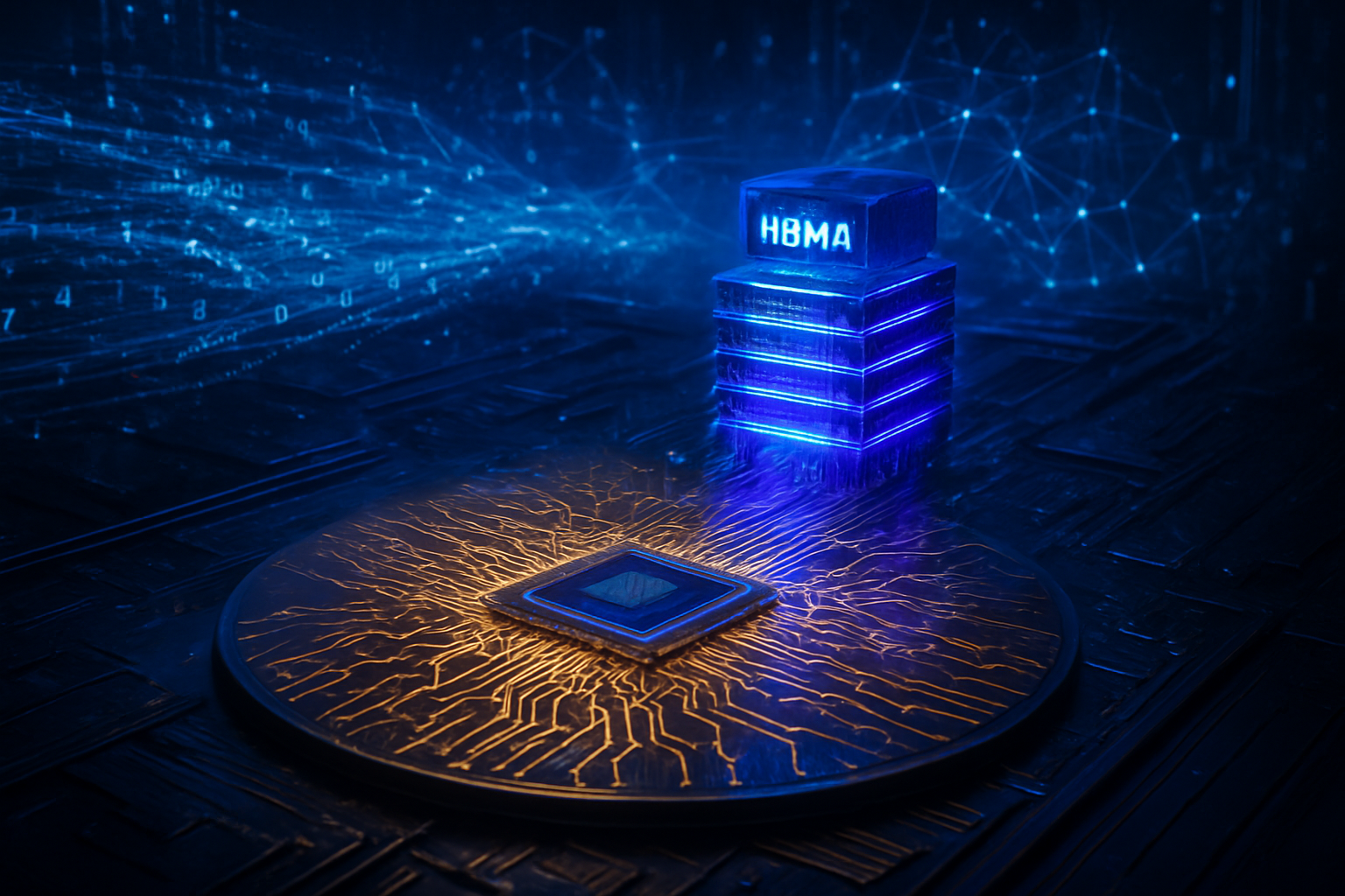
  • Navitas Semiconductor Navigates Strategic Pivot Towards High-Growth AI and EV Markets Amidst Stock Volatility

    Navitas Semiconductor Navigates Strategic Pivot Towards High-Growth AI and EV Markets Amidst Stock Volatility

    Navitas Semiconductor (NASDAQ: NVTS), a leading innovator in gallium nitride (GaN) and silicon carbide (SiC) power semiconductors, is undergoing a significant strategic transformation, dubbed "Navitas 2.0." This pivot involves shifting focus from lower-margin consumer and mobile markets to high-power, high-growth segments like AI data centers, electric vehicles (EVs), and renewable energy infrastructure. This strategic realignment has profoundly impacted its recent market performance and stock fluctuations, with investor sentiment reflecting a cautious optimism for long-term growth despite near-term financial adjustments.

    The company's stock has shown remarkable volatility, surging 165% year-to-date in 2025, even as it faces anticipated revenue declines in the immediate future due to its deliberate exit from less profitable ventures. Navitas's immediate significance lies in its crucial role in enabling more efficient power conversion, particularly in the burgeoning AI data center market, where its GaN and SiC technologies are becoming indispensable for next-generation computing infrastructure.

    GaN and SiC: Powering the Future of High-Efficiency Electronics

    Navitas Semiconductor's core strength lies in its advanced gallium nitride (GaN) and silicon carbide (SiC) power ICs and discrete components, which are at the forefront of enabling next-generation power conversion. Unlike traditional silicon-based power semiconductors, GaN and SiC offer superior performance characteristics, including higher switching speeds, lower on-resistance, and reduced energy losses. These attributes are critical for applications demanding high power density and efficiency, such as fast chargers, data center power supplies, electric vehicle powertrains, and renewable energy inverters.

    The company's "Navitas 2.0" strategy specifically targets the deployment of these advanced materials in high-power, high-growth markets. For instance, Navitas is recognized for its GaNFast™ power ICs, which integrate GaN power FETs with drive, control, and protection features into a single, monolithic device. This integration simplifies design, reduces component count, and enhances reliability, offering a distinct advantage over discrete GaN solutions. In the SiC domain, Navitas is developing and sampling high-voltage SiC modules, including 2.3kV and 3.3kV devices, specifically for demanding applications like energy storage systems and industrial electrification.

    This approach significantly differs from previous reliance on the consumer electronics market, where profit margins are typically thinner and product lifecycles shorter. By focusing on enterprise and industrial applications, Navitas aims to leverage the inherent technical advantages of GaN and SiC to address critical pain points like power density and energy efficiency in complex systems. Initial reactions from the AI research community and power electronics industry experts have been largely positive, viewing GaN and SiC as essential technologies for the future, particularly given the escalating power demands of AI data centers. The selection of Navitas as a power semiconductor partner by NVIDIA for its next-generation 800V DC architecture in AI factory computing serves as a strong validation of Navitas's technological leadership and the market's recognition of its advanced solutions.

    Market Dynamics: Beneficiaries, Competition, and Strategic Positioning

    Navitas Semiconductor's strategic pivot towards high-power GaN and SiC solutions positions it to significantly benefit from the explosive growth in several key sectors. Companies investing heavily in AI infrastructure, electric vehicles, and renewable energy stand to gain from Navitas's ability to provide more efficient and compact power conversion. Notably, hyperscale data center operators and AI hardware manufacturers, such as NVIDIA (NASDAQ: NVDA) and other developers of AI accelerators, are direct beneficiaries, as Navitas's technology helps address the critical challenges of power delivery and thermal management in increasingly dense AI computing environments. The company's partnership with NVIDIA underscores its critical role in enabling the next generation of AI factories.

    The competitive landscape for Navitas is multifaceted, involving both established semiconductor giants and other specialized GaN/SiC players. Major tech companies like Infineon (ETR: IFX, OTCQX: IFNNY), STMicroelectronics (NYSE: STM), and Wolfspeed (NYSE: WOLF) are also heavily invested in GaN and SiC technologies. However, Navitas aims to differentiate itself through its GaNFast™ IC integration approach, offering a more complete and easy-to-implement solution compared to discrete components. This could potentially disrupt existing power supply designs that rely on more complex discrete GaN or SiC implementations. For startups in the power electronics space, Navitas's advancements could either present opportunities for collaboration or intensify competition, depending on their specific niche.

    Navitas's market positioning is strengthened by its strategic focus on specific high-growth applications where GaN and SiC offer distinct advantages. By moving away from the highly commoditized consumer mobile market, the company seeks higher-margin opportunities and more stable, long-term design wins. Its expanding ecosystem, including collaborations with GlobalFoundries (NASDAQ: GFS) for U.S.-based GaN technology and WT Microelectronics (TPE: 3036) for Asian distribution, further solidifies its strategic advantages. This network of partnerships aims to accelerate GaN adoption globally and ensure a robust supply chain, crucial for scaling its solutions in demanding enterprise and industrial markets.

    Broader Implications: Powering the AI Revolution and Beyond

    Navitas Semiconductor's advancements in GaN and SiC power semiconductors are not merely incremental improvements; they represent a fundamental shift in how power is managed in the broader AI landscape and other critical sectors. The increasing demand for computational power in AI, particularly for training large language models and running complex inference tasks, has led to a significant surge in energy consumption within data centers. Traditional silicon-based power solutions are reaching their limits in terms of efficiency and power density. GaN and SiC technologies, with their superior switching characteristics and reduced energy losses, are becoming indispensable for addressing this energy crisis, enabling smaller, lighter, and more efficient power supplies that can handle the extreme power requirements of AI accelerators.

    The impact of this shift extends far beyond data centers. In electric vehicles, GaN and SiC enable more efficient inverters and on-board chargers, leading to increased range and faster charging times. In renewable energy, they improve the efficiency of solar microinverters and energy storage systems, crucial for grid modernization and decarbonization efforts. These developments fit perfectly into broader trends of electrification, digitalization, and the pursuit of sustainability across industries.

    However, the widespread adoption of GaN and SiC also presents potential concerns. The supply chain for these relatively newer materials is still maturing compared to silicon, and any disruptions could impact production. Furthermore, the cost premium associated with GaN and SiC, while decreasing, can still be a barrier for some applications. Despite these challenges, the current trajectory suggests that GaN and SiC are on par with previous semiconductor milestones, such as the transition from germanium to silicon, in terms of their potential to unlock new levels of performance and efficiency. Their role in enabling the current AI revolution, which is heavily dependent on efficient power delivery, underscores their significance as a foundational technology for the next wave of technological innovation.

    The Road Ahead: Anticipated Developments and Challenges

    The future for Navitas Semiconductor, and indeed for the broader GaN and SiC power semiconductor market, is characterized by anticipated rapid growth and continuous innovation. In the near-term, Navitas expects to complete its strategic pivot, with management projecting Q4 2025 revenues to be the lowest point as it sheds lower-margin businesses. However, a healthier growth rate is expected to resume in late 2025 and accelerate significantly through 2027 and 2028, with substantial contributions from AI data centers and EV markets. The company's bidirectional GaN ICs, GaN BDS, launched in early 2025, are expected to ramp up in solar microinverters by late 2025, indicating new product cycles coming online.

    Long-term developments include the increasing adoption of 800-volt equipment in data centers, starting in 2026 and accelerating through 2030, which Navitas is well-positioned to capitalize on with its GaN and SiC solutions. Experts predict that the overall GaN and SiC device markets will continue robust annualized growth of 25% through 2032, highlighting the sustained demand for these efficient power technologies. Potential applications on the horizon include more advanced power solutions for robotics, industrial automation, and even future aerospace applications, where weight and efficiency are paramount.

    However, several challenges need to be addressed. Scaling manufacturing to meet the anticipated demand, further reducing the cost of GaN and SiC devices, and educating the broader engineering community on their optimal design and implementation are crucial. Competition from other wide-bandgap materials and ongoing advancements in silicon-based technologies could also pose challenges. Despite these hurdles, experts predict that the undeniable performance benefits and efficiency gains offered by GaN and SiC will drive their continued integration into critical infrastructure. What to watch for next includes Navitas's revenue rebound in 2027 and beyond, further strategic partnerships, and the expansion of its product portfolio into even higher power and voltage applications.

    Navitas's Strategic Resurgence: A New Era for Power Semiconductors

    Navitas Semiconductor's journey through 2025 and into the future marks a pivotal moment in the power semiconductor industry. The company's "Navitas 2.0" strategy, a decisive shift from low-margin consumer electronics to high-growth, high-power applications like AI data centers, EVs, and renewable energy, is a clear recognition of the evolving demands for energy efficiency and power density. While this transition has introduced near-term revenue pressures and stock volatility, the significant year-to-date stock surge of 165% reflects strong investor confidence in its long-term vision and its foundational role in powering the AI revolution.

    This development is profoundly significant in AI history, as the efficiency of power delivery is becoming as critical as computational power itself. Navitas's GaN and SiC technologies are not just components; they are enablers of the next generation of AI infrastructure, allowing for more powerful, compact, and sustainable computing. The validation from industry leaders like NVIDIA underscores the transformative potential of these materials. The challenges of scaling production, managing costs, and navigating a competitive landscape remain, but Navitas's strong cash position and strategic partnerships provide a solid foundation for continued innovation and market penetration.

    In the coming weeks and months, observers should closely watch for Navitas's Q4 2025 results as the anticipated low point in its revenue trajectory. Subsequent quarters will be crucial indicators of the success of its strategic pivot and the ramp-up of its GaN and SiC solutions in key markets. Further announcements regarding partnerships, new product introductions, and design wins in AI data centers, EVs, and renewable energy will provide insights into the company's progress and its long-term impact on the global energy and technology landscape. Navitas Semiconductor is not just riding the wave of technological change; it is actively shaping the future of efficient power.


    This content is intended for informational purposes only and represents analysis of current AI developments.

    TokenRing AI delivers enterprise-grade solutions for multi-agent AI workflow orchestration, AI-powered development tools, and seamless remote collaboration platforms.
    For more information, visit https://www.tokenring.ai/.