Blog

  • The AI Supercycle: Unpacking the Trillion-Dollar Semiconductor Surge Fueling the Future of Intelligence

    The AI Supercycle: Unpacking the Trillion-Dollar Semiconductor Surge Fueling the Future of Intelligence

    As of October 2025, the global semiconductor market is not just experiencing a boom; it's undergoing a profound, structural transformation dubbed the "AI Supercycle." This unprecedented surge, driven by the insatiable demand for artificial intelligence, is repositioning semiconductors as the undisputed lifeblood of a burgeoning global AI economy. With global semiconductor sales projected to hit approximately $697 billion in 2025—an impressive 11% year-over-year increase—the industry is firmly on an ambitious trajectory towards a staggering $1 trillion valuation by 2030, and potentially even $2 trillion by 2040.

    The immediate significance of this trend cannot be overstated. The massive capital flowing into the sector signals a fundamental re-architecture of global technological infrastructure. Investors, governments, and tech giants are pouring hundreds of billions into expanding manufacturing capabilities and developing next-generation AI-specific hardware, recognizing that the very foundation of future AI advancements rests squarely on the shoulders of advanced silicon. This isn't merely a cyclical market upturn; it's a strategic global race to build the computational backbone for the age of artificial intelligence.

    Investment Tides and Technological Undercurrents in the Silicon Sea

    The detailed technical coverage of current investment trends reveals a highly dynamic landscape. Companies are slated to inject around $185 billion into capital expenditures in 2025, primarily to boost global manufacturing capacity by a significant 7%. However, this investment isn't evenly distributed; it's heavily concentrated among a few titans, notably Taiwan Semiconductor Manufacturing Company (TSMC) (NYSE: TSM) and Micron Technology (NASDAQ: MU). Excluding these major players, overall semiconductor CapEx for 2025 would actually show a 10% decrease from 2024, highlighting the targeted nature of AI-driven investment.

    Crucially, strategic government funding initiatives are playing a pivotal role in shaping this investment landscape. Programs such as the U.S. CHIPS and Science Act, Europe's European Chips Act, and similar efforts across Asia are channeling hundreds of billions into private-sector investments. These acts aim to bolster supply chain resilience, mitigate geopolitical risks, and secure technological leadership, further accelerating the semiconductor industry's expansion. This blend of private capital and public policy is creating a robust, if geographically fragmented, investment environment.

    Major semiconductor-focused Exchange Traded Funds (ETFs) reflect this bullish sentiment. The VanEck Semiconductor ETF (SMH), for instance, has demonstrated robust performance, climbing approximately 39% year-to-date as of October 2025, and earning a "Moderate Buy" rating from analysts. Its strong performance underscores investor confidence in the sector's long-term growth prospects, driven by the relentless demand for high-performance computing, memory solutions, and, most critically, AI-specific chips. This sustained upward momentum in ETFs indicates a broad market belief in the enduring nature of the AI Supercycle.

    Nvidia and TSMC: Architects of the AI Era

    The impact of these trends on AI companies, tech giants, and startups is profound, with Nvidia (NASDAQ: NVDA) and TSMC (NYSE: TSM) standing at the epicenter. Nvidia has solidified its position as the world's most valuable company, with its market capitalization soaring past an astounding $4.5 trillion by early October 2025, and its stock climbing approximately 39% year-to-date. An astonishing 88% of Nvidia's latest quarterly revenue, with data center revenue accounting for nearly 90% of the total, is now directly attributable to AI sales, driven by overwhelming demand for its GPUs from cloud service providers and enterprises. The company's strategic moves, including the unveiling of NVLink Fusion for flexible AI system building, Mission Control for data center management, and a shift towards a more open AI infrastructure ecosystem, underscore its ambition to maintain its estimated 80% share of the enterprise AI chip market. Furthermore, Nvidia's next-generation Blackwell AI chips (GeForce RTX 50 Series), boasting 92 billion transistors and 3,352 trillion AI operations per second, are already securing over 70% of TSMC's advanced chip packaging capacity for 2025.

    TSMC, the undisputed global leader in foundry services, crossed the $1 trillion market capitalization threshold in July 2025, with AI-related applications contributing a substantial 60% to its Q2 2025 revenue. The company is dedicating approximately 70% of its 2025 capital expenditures to advanced process technologies, demonstrating its commitment to staying at the forefront of chip manufacturing. To meet the surging demand for AI chips, TSMC is aggressively expanding its CoWoS (Chip-on-Wafer-on-Substrate) advanced packaging production capacity, aiming to quadruple it from approximately 36,000 wafers per month to 90,000 by the end of 2025, and further to 130,000 per month by 2026. This monumental expansion, coupled with plans for volume production of its cutting-edge 2nm process in late 2025 and the construction of nine new facilities globally, cements TSMC's critical role as the foundational enabler of the AI chip ecosystem.

    While Nvidia and TSMC dominate, the competitive landscape is evolving. Other major players like Advanced Micro Devices (NASDAQ: AMD) and Intel Corporation (NASDAQ: INTC) are aggressively pursuing their own AI chip strategies, while hyperscalers such as Alphabet (NASDAQ: GOOGL) (with its TPUs), Amazon (NASDAQ: AMZN) (with Trainium), and Microsoft (NASDAQ: MSFT) (with Maia) are developing custom silicon. This competitive pressure is expected to see these challengers collectively capture 15-20% of the AI chip market, potentially disrupting Nvidia's near-monopoly and offering diverse options for AI labs and startups. The intense focus on custom and specialized AI hardware signifies a strategic advantage for companies that can optimize their AI models directly on purpose-built silicon, potentially leading to significant performance and cost efficiencies.

    The Broader Canvas: AI's Demand for Silicon Innovation

    The wider significance of these semiconductor investment trends extends deep into the broader AI landscape. Investor sentiment remains overwhelmingly optimistic, viewing the industry as undergoing a fundamental re-architecture driven by the "AI Supercycle." This period is marked by an accelerating pace of technological advancements, essential for meeting the escalating demands of AI workloads. Beyond traditional CPUs and general-purpose GPUs, specialized chip architectures are emerging as critical differentiators.

    Key innovations include neuromorphic computing, exemplified by Intel's Loihi 2 and IBM's TrueNorth, which mimic the human brain for ultra-low power consumption and efficient pattern recognition. Advanced packaging technologies like TSMC's CoWoS and Applied Materials' Kinex hybrid bonding system are crucial for integrating multiple chiplets into complex, high-performance AI systems, optimizing for power, performance, and cost. High-Bandwidth Memory (HBM) is another critical component, with its market revenue projected to reach $21 billion in 2025, a 70% year-over-year increase, driven by intense focus from companies like Samsung (KRX: 005930) on HBM4 development. The rise of Edge AI and distributed processing is also significant, with AI-enabled PCs expected to constitute 43% of all shipments by the end of 2025, as companies like Microsoft and Apple (NASDAQ: AAPL) integrate AI directly into operating systems and devices. Furthermore, innovations in cooling solutions, such as Microsoft's microfluidics breakthrough, are becoming essential for managing the immense heat generated by powerful AI chips, and AI itself is increasingly being used as a tool in chip design, accelerating innovation cycles.

    Despite the euphoria, potential concerns loom. Some analysts predict a possible slowdown in AI chip demand growth between 2026 and 2027 as hyperscalers might moderate their initial massive infrastructure investments. Geopolitical influences, skilled worker shortages, and the inherent complexities of global supply chains also present ongoing challenges. However, the overarching comparison to previous technological milestones, such as the internet boom or the mobile revolution, positions the current AI-driven semiconductor surge as a foundational shift with far-reaching societal and economic impacts. The ability of the industry to navigate these challenges will determine the long-term sustainability of the AI Supercycle.

    The Horizon: Anticipating AI's Next Silicon Frontier

    Looking ahead, the global AI chip market is forecast to surpass $150 billion in sales in 2025, with some projections reaching nearly $300 billion by 2030, and data center AI chips potentially exceeding $400 billion. The data center market, particularly for GPUs, HBM, SSDs, and NAND, is expected to be the primary growth engine, with semiconductor sales in this segment projected to grow at an impressive 18% Compound Annual Growth Rate (CAGR) from $156 billion in 2025 to $361 billion by 2030. This robust outlook highlights the sustained demand for specialized hardware to power increasingly complex AI models and applications.

    Expected near-term and long-term developments include continued innovation in specialized chip architectures, with a strong emphasis on energy efficiency and domain-specific acceleration. Emerging technologies such as photonic computing, quantum computing components, and further advancements in heterogeneous integration are on the horizon, promising even greater computational power. Potential applications and use cases are vast, spanning from fully autonomous systems and hyper-personalized AI services to scientific discovery and advanced robotics.

    However, significant challenges need to be addressed. Scaling manufacturing to meet demand, managing the escalating power consumption and heat dissipation of advanced chips, and controlling the spiraling costs of fabrication are paramount. Experts predict that while Nvidia will likely maintain its leadership, competition will intensify, with AMD, Intel, and custom silicon from hyperscalers potentially capturing a larger market share. Some analysts also caution about a potential "first plateau" in AI chip demand between 2026-2027 and a "second critical period" around 2028-2030 if profitable use cases don't sufficiently develop to justify the massive infrastructure investments. The industry's ability to demonstrate tangible returns on these investments will be crucial for sustaining momentum.

    The Enduring Legacy of the Silicon Supercycle

    In summary, the current investment trends in the semiconductor market unequivocally signal the reality of the "AI Supercycle." This period is characterized by unprecedented capital expenditure, strategic government intervention, and a relentless drive for technological innovation, all fueled by the escalating demands of artificial intelligence. Key players like Nvidia and TSMC are not just beneficiaries but are actively shaping this new era through their dominant market positions, massive investments in R&D, and aggressive capacity expansions. Their strategic moves in advanced packaging, next-generation process nodes, and integrated AI platforms are setting the pace for the entire industry.

    The significance of this development in AI history is monumental, akin to the foundational shifts brought about by the internet and mobile revolutions. Semiconductors are no longer just components; they are the strategic assets upon which the global AI economy will be built, enabling breakthroughs in machine learning, large language models, and autonomous systems. The long-term impact will be a fundamentally reshaped technological landscape, with AI deeply embedded across all industries and aspects of daily life.

    What to watch for in the coming weeks and months includes continued announcements regarding manufacturing capacity expansions, the rollout of new chip architectures from competitors, and further strategic partnerships aimed at solidifying market positions. Investors should also pay close attention to the development of profitable AI use cases that can justify the massive infrastructure investments and to any shifts in geopolitical dynamics that could impact global supply chains. The AI Supercycle is here, and its trajectory will define the future of intelligence.


    This content is intended for informational purposes only and represents analysis of current AI developments.

    TokenRing AI delivers enterprise-grade solutions for multi-agent AI workflow orchestration, AI-powered development tools, and seamless remote collaboration platforms.
    For more information, visit https://www.tokenring.ai/.

  • Green AI’s Dawn: Organic Semiconductors Unleash a New Era of Sustainable Energy for Computing

    Green AI’s Dawn: Organic Semiconductors Unleash a New Era of Sustainable Energy for Computing

    October 7, 2025 – A quiet revolution is brewing at the intersection of materials science and artificial intelligence, promising to fundamentally alter how the world's most demanding computational tasks are powered. Recent breakthroughs in organic semiconductors, particularly in novel directed co-catalyst deposition for photocatalytic hydrogen production, are poised to offer a viable pathway toward truly sustainable AI. This development arrives at a critical juncture, as the energy demands of AI models and data centers escalate, making the pursuit of green AI not just an environmental imperative but an economic necessity.

    The most significant advancement, reported by the Chinese Academy of Sciences (CAS) and announced today, demonstrates an unprecedented leap in efficiency for generating hydrogen fuel using only sunlight and organic materials. This innovation, coupled with other pioneering efforts in bio-inspired energy systems, signals a profound shift from energy-intensive AI to an era where intelligence can thrive sustainably, potentially transforming the entire tech industry's approach to power.

    Technical Marvels: Precision Engineering for Green Hydrogen

    The breakthrough from the Chinese Academy of Sciences (CAS), led by Yuwu Zhong's team at the Institute of Chemistry in collaboration with the University of Science and Technology of China, centers on a sophisticated method for directed co-catalyst deposition on organic semiconductor heterojunctions. Published in CCS Chem. in August 2025, their technique involves using a bifunctional organic small molecule, 1,3,6,8-tetrakis(di(p-pyridin-4-phenyl)amino)pyrene (TAPyr), to form stable heterojunctions with graphitic carbon nitride (CN). Crucially, the polypyridine terminal groups of TAPyr act as molecular anchoring sites, enabling the uniform and precise deposition of platinum (Pt) nanoparticles. This precision is paramount, as it optimizes the catalytic activity by ensuring ideal integration between the co-catalyst and the semiconductor.

    This novel approach has yielded remarkable results, demonstrating a maximum hydrogen evolution rate of 6.6 mmol·h⁻¹·gcat⁻¹ under visible light, translating to an apparent rate of 660 mmol·h⁻¹·gPt⁻¹ when normalized to the added Pt precursor. This represents an efficiency more than 30 times higher than that of a single-component CN system, along with excellent stability for nearly 90 hours. This method directly addresses long-standing challenges in organic semiconductors, such as limited exciton diffusion lengths and high Frenkel exciton binding energies, which have historically hindered efficient charge separation and transfer. By facilitating better integration and enhancing charge dynamics, this directed deposition strategy unlocks new levels of performance for organic photocatalysts.

    Complementing this, researchers at the University of Liverpool, led by Professor Luning Liu and Professor Andy Cooper, unveiled a light-powered hybrid nanoreactor in December 2024. This innovative system combines recombinant α-carboxysome shells (natural microcompartments from bacteria) with a microporous organic semiconductor. The carboxysome shells elegantly protect sensitive hydrogenase enzymes—highly efficient hydrogen producers that are typically vulnerable to oxygen deactivation. The microporous organic semiconductor acts as a light-harvesting antenna, absorbing visible light and transferring excitons to the biocatalyst to drive hydrogen production. This bio-inspired design mimics natural photosynthesis, offering a cost-effective alternative to traditional synthetic photocatalysts by reducing or eliminating the reliance on expensive precious metals, while achieving comparable efficiency.

    Reshaping the AI Industry: A Sustainable Competitive Edge

    These advancements in organic semiconductors and photocatalytic hydrogen production carry profound implications for AI companies, tech giants, and startups alike. Companies heavily invested in AI infrastructure, such as cloud providers Amazon (NASDAQ: AMZN) AWS, Microsoft (NASDAQ: MSFT) Azure, and Alphabet (NASDAQ: GOOGL) Google Cloud, stand to gain significantly. The ability to generate clean, on-site hydrogen could drastically reduce their operational expenditures associated with powering massive data centers, which are projected to triple their power consumption by 2030, with AI workloads consuming 10 to 30 times more electricity than traditional computing tasks.

    For AI hardware manufacturers like NVIDIA (NASDAQ: NVDA), Intel (NASDAQ: INTC), and AMD (NASDAQ: AMD), the availability of sustainable energy sources could accelerate the development of more powerful, yet environmentally responsible, processors and accelerators. A "greener silicon" paradigm, supported by clean energy, could become a key differentiator. Startups focused on green tech, energy management, and advanced materials could find fertile ground for innovation, developing new solutions to integrate hydrogen production and fuel cell technology directly into AI infrastructure.

    The competitive landscape will undoubtedly shift. Companies that proactively invest in and adopt these sustainable energy solutions will not only bolster their environmental, social, and governance (ESG) credentials but also secure a strategic advantage through reduced energy costs and increased energy independence. This development has the potential to disrupt existing energy supply chains for data centers, fostering a move towards more localized and renewable power generation, thereby enhancing resilience and sustainability across the entire AI ecosystem.

    A New Pillar in the Broader AI Landscape

    These breakthroughs fit seamlessly into the broader AI landscape, addressing one of its most pressing challenges: the escalating environmental footprint. As AI models become larger and more complex, their energy consumption grows proportionally, raising concerns about their long-term sustainability. Efficient photocatalytic hydrogen production offers a tangible solution, providing a clean fuel source that can power the next generation of AI systems without exacerbating climate change. This moves beyond mere energy efficiency optimizations within algorithms or hardware, offering a fundamental shift in the energy supply itself.

    The impacts are far-reaching. Beyond reducing carbon emissions, widespread adoption of green hydrogen for AI could stimulate significant investment in renewable energy infrastructure, create new green jobs, and reduce reliance on fossil fuels. While the promise is immense, potential concerns include the scalability of these technologies to meet the colossal demands of global AI infrastructure, the long-term stability of organic materials under continuous operation, and the safe and efficient storage and distribution of hydrogen. Nevertheless, this milestone stands alongside other significant AI advancements, such as the development of energy-efficient large language models and neuromorphic computing, as a critical step towards a more environmentally responsible technological future.

    The Horizon: Integrated Sustainable AI Ecosystems

    Looking ahead, the near-term developments will likely focus on optimizing the efficiency and durability of these organic semiconductor systems, as well as scaling up production processes. Pilot projects integrating green hydrogen production directly into data center operations are expected to emerge, providing real-world validation of the technology's viability. Researchers will continue to explore novel organic materials and co-catalyst strategies, pushing the boundaries of hydrogen evolution rates and stability.

    In the long term, experts predict the commercialization of modular, decentralized hydrogen production units powered by organic photocatalysts, enabling AI facilities to generate their own clean energy. This could lead to the development of fully integrated AI-powered energy management systems, where AI itself optimizes hydrogen production, storage, and consumption for its own operational needs. Challenges remain, particularly in achieving cost parity with traditional energy sources at scale, ensuring long-term material stability, and developing robust hydrogen storage and transportation infrastructure. However, the trajectory is clear: a future where AI is powered by its own sustainably generated fuel.

    A Defining Moment for Green AI

    The recent breakthroughs in organic semiconductors and directed co-catalyst deposition for photocatalytic hydrogen production mark a defining moment in the quest for green AI. The work by the Chinese Academy of Sciences, complemented by innovations like the University of Liverpool's hybrid nanoreactor, provides concrete, high-efficiency pathways to generate clean hydrogen fuel from sunlight using cost-effective and scalable organic materials. This is not merely an incremental improvement; it is a foundational shift that promises to decouple AI's growth from its environmental impact.

    The significance of this development in AI history cannot be overstated. It represents a critical step towards mitigating the escalating energy demands of artificial intelligence, offering a vision of AI that is not only powerful and transformative but also inherently sustainable. As the tech industry continues its relentless pursuit of advanced intelligence, the ability to power this intelligence responsibly will be paramount. In the coming weeks and months, the world will be watching for further efficiency gains, the first large-scale pilot deployments, and the policy frameworks that will support the integration of these groundbreaking energy solutions into the global AI infrastructure. The era of truly green AI is dawning.

    This content is intended for informational purposes only and represents analysis of current AI developments.

    TokenRing AI delivers enterprise-grade solutions for multi-agent AI workflow orchestration, AI-powered development tools, and seamless remote collaboration platforms. For more information, visit https://www.tokenring.ai/.

  • Advanced Energy Unveils Game-Changing Mid-Infrared Pyrometer: A New Era for Precision AI Chip Manufacturing

    Advanced Energy Unveils Game-Changing Mid-Infrared Pyrometer: A New Era for Precision AI Chip Manufacturing

    October 7, 2025 – In a significant leap forward for semiconductor manufacturing, Advanced Energy Industries, Inc. (NASDAQ: AEIS) today announced the launch of its revolutionary 401M Mid-Infrared Pyrometer. Debuting at SEMICON® West 2025, this cutting-edge optical pyrometer promises to redefine precision temperature control in the intricate processes essential for producing the next generation of advanced AI chips. With AI’s insatiable demand for more powerful and efficient hardware, the 401M arrives at a critical juncture, offering unprecedented accuracy and speed that could dramatically enhance yields and accelerate the development of sophisticated AI processors.

    The 401M Mid-Infrared Pyrometer is poised to become an indispensable tool in the fabrication of high-performance semiconductors, particularly those powering the rapidly expanding artificial intelligence ecosystem. Its ability to deliver real-time, non-contact temperature measurements with exceptional precision and speed directly addresses some of the most pressing challenges in advanced chip manufacturing. As the industry pushes the boundaries of Moore's Law, the reliability and consistency of processes like epitaxy and chemical vapor deposition (CVD) are paramount, and Advanced Energy's latest innovation stands ready to deliver the meticulous control required for the complex architectures of future AI hardware.

    Unpacking the Technological Marvel: Precision Redefined for AI Silicon

    The Advanced Energy 401M Mid-Infrared Pyrometer represents a substantial technical advancement in process control instrumentation. At its core, the device offers an impressive accuracy of ±3°C across a wide temperature range of 50°C to 1,300°C, coupled with a lightning-fast response time as low as 1 microsecond. This combination of precision and speed is critical for real-time closed-loop control in highly dynamic semiconductor manufacturing environments.

    What truly sets the 401M apart is its reliance on mid-infrared (1.7 µm to 5.2 µm spectral range) technology. Unlike traditional near-infrared pyrometers, the mid-infrared range allows for more accurate and stable measurements through transparent surfaces and outside the immediate process environment, circumventing interferences that often plague conventional methods. This makes it exceptionally well-suited for demanding applications such as lamp-heated epitaxy, CVD, and thin-film glass coating processes, which are foundational to creating the intricate layers of modern AI chips. Furthermore, the 401M boasts integrated EtherCAT® communication, simplifying tool integration by eliminating the need for external modules and enhancing system reliability. It also supports USB, Serial, and analog data interfaces for broad compatibility.

    This innovative approach significantly differs from previous generations of pyrometers, which often struggled with the complexities of measuring temperatures through evolving film layers or in the presence of challenging optical interferences. By providing customizable measurement wavelengths, temperature ranges, and working distances, along with automatic ambient thermal correction, the 401M offers unparalleled flexibility. While initial reactions from the AI research community and industry experts are just beginning to surface given today's announcement, the consensus is likely to highlight the pyrometer's potential to unlock new levels of process stability and yield, particularly for sub-7nm process nodes crucial for advanced AI accelerators. The ability to maintain such tight thermal control is a game-changer for fabricating high-density, multi-layer AI processors.

    Reshaping the AI Chip Landscape: Strategic Advantages and Market Implications

    The introduction of Advanced Energy's 401M Mid-Infrared Pyrometer carries profound implications for AI companies, tech giants, and startups operating in the semiconductor space. Companies at the forefront of AI chip design and manufacturing, such as NVIDIA (NASDAQ: NVDA), Intel (NASDAQ: INTC), Taiwan Semiconductor Manufacturing Company (TSMC) (NYSE: TSM), and Samsung Electronics (KRX: 005930), stand to benefit immensely. These industry leaders are constantly striving for higher yields, improved performance, and reduced manufacturing costs in their pursuit of ever more powerful AI accelerators. The 401M's enhanced precision in critical processes like epitaxy and CVD directly translates into better quality wafers and a higher number of functional chips per wafer, providing a significant competitive advantage.

    For major AI labs and tech companies that rely on custom or leading-edge AI silicon, this development means potentially faster access to more reliable and higher-performing chips. The improved process control offered by the 401M could accelerate the iteration cycles for new chip designs, enabling quicker deployment of advanced AI models and applications. This could disrupt existing products or services by making advanced AI hardware more accessible and cost-effective to produce, potentially lowering the barrier to entry for certain AI applications that previously required prohibitively expensive custom silicon.

    In terms of market positioning and strategic advantages, companies that adopt the 401M early could gain a significant edge in the race to produce the most advanced and efficient AI hardware. For example, a foundry like TSMC, which manufactures chips for a vast array of AI companies, could leverage this technology to further solidify its leadership in advanced node production. Similarly, integrated device manufacturers (IDMs) like Intel, which designs and fabricates its own AI processors, could see substantial improvements in their manufacturing efficiency and product quality. The ability to consistently produce high-quality AI chips at scale is a critical differentiator in a market experiencing explosive growth and intense competition.

    Broader AI Significance: Pushing the Boundaries of What's Possible

    The launch of the Advanced Energy 401M Mid-Infrared Pyrometer fits squarely into the broader AI landscape as a foundational enabler for future innovation. As AI models grow exponentially in size and complexity, the demand for specialized hardware capable of handling massive computational loads continues to surge. This pyrometer is not merely an incremental improvement; it represents a critical piece of the puzzle in scaling AI capabilities by ensuring the manufacturing quality of the underlying silicon. It addresses the fundamental need for precision at the atomic level, which is becoming increasingly vital as chip features shrink to just a few nanometers.

    The impacts are wide-ranging. From accelerating research into novel AI architectures to making existing AI solutions more powerful and energy-efficient, the ability to produce higher-quality, more reliable AI chips is transformative. It allows for denser transistor packing, improved power delivery, and enhanced signal integrity – all crucial for AI accelerators. Potential concerns, however, might include the initial cost of integrating such advanced technology into existing fabrication lines and the learning curve associated with optimizing its use. Nevertheless, the long-term benefits in terms of yield improvement and performance gains are expected to far outweigh these initial hurdles.

    Comparing this to previous AI milestones, the 401M might not be a direct AI algorithm breakthrough, but it is an essential infrastructural breakthrough. It parallels advancements in lithography or material science that, while not directly AI, are absolutely critical for AI's progression. Just as better compilers enabled more complex software, better manufacturing tools enable more complex hardware. This development is akin to optimizing the very bedrock upon which all future AI innovations will be built, ensuring that the physical limitations of silicon do not impede the relentless march of AI progress.

    The Road Ahead: Anticipating Future Developments and Applications

    Looking ahead, the Advanced Energy 401M Mid-Infrared Pyrometer is expected to drive both near-term and long-term developments in semiconductor manufacturing and, by extension, the AI industry. In the near term, we can anticipate rapid adoption by leading-edge foundries and IDMs as they integrate the 401M into their existing and upcoming fabrication lines. This will likely lead to incremental but significant improvements in the yield and performance of current-generation AI chips, particularly those manufactured at 5nm and 3nm nodes. The immediate focus will be on optimizing its use in critical deposition and epitaxy processes to maximize its impact on chip quality and throughput.

    In the long term, the capabilities offered by the 401M could pave the way for even more ambitious advancements. Its precision and ability to measure through challenging environments could facilitate the development of novel materials and 3D stacking technologies for AI chips, where thermal management and inter-layer connection quality are paramount. Potential applications include enabling the mass production of neuromorphic chips, in-memory computing architectures, and other exotic AI hardware designs that require unprecedented levels of manufacturing control. Challenges that need to be addressed include further miniaturization of the pyrometer for integration into increasingly complex process tools, as well as developing advanced AI-driven feedback loops that can fully leverage the 401M's real-time data for autonomous process optimization.

    Experts predict that this level of precise process control will become a standard requirement for all advanced semiconductor manufacturing. The continuous drive towards smaller feature sizes and more complex chip architectures for AI demands nothing less. What's next could involve the integration of AI directly into the pyrometer's analytics, predicting potential process deviations before they occur, or even dynamic, self-correcting manufacturing environments where temperature is maintained with absolute perfection through machine learning algorithms.

    A New Benchmark in AI Chip Production: The 401M's Enduring Legacy

    In summary, Advanced Energy's new 401M Mid-Infrared Pyrometer marks a pivotal moment in semiconductor process control, offering unparalleled precision and speed in temperature measurement. Its mid-infrared technology and robust integration capabilities are specifically tailored to address the escalating demands of advanced chip manufacturing, particularly for the high-performance AI processors that are the backbone of modern artificial intelligence. The key takeaway is that this technology directly contributes to higher yields, improved chip quality, and faster innovation cycles for AI hardware.

    This development's significance in AI history cannot be overstated. While not an AI algorithm itself, it is a critical enabler, providing the foundational manufacturing excellence required to bring increasingly complex and powerful AI chips from design to reality. Without such advancements in process control, the ambitious roadmaps for AI hardware would face insurmountable physical limitations. The 401M helps ensure that the physical world of silicon can keep pace with the exponential growth of AI's computational demands.

    Our final thoughts underscore that this is more than just a new piece of equipment; it represents a commitment to pushing the boundaries of what is manufacturable in the AI era. Its long-term impact will be seen in the improved performance, energy efficiency, and accessibility of AI technologies across all sectors. In the coming weeks and months, we will be watching closely for adoption rates among major foundries and chipmakers, as well as any announcements regarding the first AI chips produced with the aid of this groundbreaking technology. The 401M is not just measuring temperature; it's measuring the future of AI.


    This content is intended for informational purposes only and represents analysis of current AI developments.

    TokenRing AI delivers enterprise-grade solutions for multi-agent AI workflow orchestration, AI-powered development tools, and seamless remote collaboration platforms. For more information, visit https://www.tokenring.ai/.

  • GS Microelectronics US Acquires Muse Semiconductor, Reshaping AI Chip Landscape

    GS Microelectronics US Acquires Muse Semiconductor, Reshaping AI Chip Landscape

    In a significant move poised to redefine the semiconductor and artificial intelligence industries, GS Microelectronics US (NASDAQ: GSME) officially announced its acquisition of Muse Semiconductor on October 1, 2025. This strategic consolidation marks a pivotal moment in the ongoing "AI supercycle," as industry giants scramble to secure and enhance the foundational hardware critical for advanced AI development. The acquisition is not merely a corporate merger; it represents a calculated maneuver to streamline the notoriously complex path from silicon prototype to mass production, particularly for the specialized chips powering the next generation of AI.

    The immediate implications of this merger are profound, promising to accelerate innovation across the AI ecosystem. By integrating Muse Semiconductor's agile, low-volume fabrication services—renowned for their multi-project wafer (MPW) capabilities built on TSMC technology—with GS Microelectronics US's expansive global reach and comprehensive design-to-production platform, the combined entity aims to create a single, trusted conduit for innovators. This consolidation is expected to empower a diverse range of players, from university researchers pushing the boundaries of AI algorithms to Fortune 500 companies developing cutting-edge AI infrastructure, by offering an unprecedentedly seamless transition from ideation to high-volume manufacturing.

    Technical Synergy: A New Era for AI Chip Prototyping and Production

    The acquisition of Muse Semiconductor by GS Microelectronics US is rooted in a compelling technical synergy designed to address critical bottlenecks in semiconductor development, especially pertinent to the demands of AI. Muse Semiconductor has carved out a niche as a market leader in providing agile fabrication services, leveraging TSMC's advanced process technologies for multi-project wafers (MPW). This capability is crucial for rapid prototyping and iterative design, allowing multiple chip designs to be fabricated on a single wafer, significantly reducing costs and turnaround times for early-stage development. This approach is particularly valuable for AI startups and research institutions that require quick iterations on novel AI accelerator architectures and specialized neural network processors.

    GS Microelectronics US, on the other hand, brings to the table its vast scale, extensive global customer base, and a robust, end-to-end design-to-production platform. This encompasses everything from advanced intellectual property (IP) blocks and design tools to sophisticated manufacturing processes and supply chain management. The integration of Muse's MPW expertise with GSME's high-volume production capabilities creates a streamlined "prototype-to-production" pathway that was previously fragmented. Innovators can now theoretically move from initial concept validation on Muse's agile services directly into GSME's mass production pipelines without the logistical and technical hurdles often associated with switching foundries or service providers. This unified approach is a significant departure from previous models, where developers often had to navigate multiple vendors, each with their own processes and requirements, leading to delays and increased costs.

    Initial reactions from the AI research community and industry experts have been largely positive. Many see this as a strategic move to democratize access to advanced silicon, especially for AI-specific hardware. The ability to rapidly prototype and then seamlessly scale production is considered a game-changer for AI chip development, where the pace of innovation demands constant experimentation and quick market deployment. Experts highlight that this consolidation could significantly reduce the barrier to entry for new AI hardware companies, fostering a more dynamic and competitive landscape for AI acceleration. Furthermore, it strengthens the TSMC ecosystem, which is foundational for many leading-edge AI chips, by offering a more integrated service layer.

    Market Dynamics: Reshaping Competition and Strategic Advantage in AI

    This acquisition by GS Microelectronics US (NASDAQ: GSME) is set to significantly reshape competitive dynamics within the AI and semiconductor industries. Companies poised to benefit most are those developing cutting-edge AI applications that require custom or highly optimized silicon. Startups and mid-sized AI firms, which previously struggled with the high costs and logistical complexities of moving from proof-of-concept to scalable hardware, will find a more accessible and integrated pathway to market. This could lead to an explosion of new AI hardware innovations, as the friction associated with silicon realization is substantially reduced.

    For major AI labs and tech giants like Alphabet (NASDAQ: GOOGL), Microsoft (NASDAQ: MSFT), and Amazon (NASDAQ: AMZN) that are heavily investing in custom AI chips (e.g., Google's TPUs, Amazon's Inferentia), this consolidation offers a more robust and streamlined supply chain option. While these giants often have their own internal design teams, access to an integrated service provider that can handle both agile prototyping and high-volume production, particularly within the TSMC ecosystem, provides greater flexibility and potentially faster iteration cycles for their specialized AI hardware. This could accelerate their ability to deploy more efficient and powerful AI models, further solidifying their competitive advantage in cloud AI services and autonomous systems.

    The competitive implications extend to existing foundry services and other semiconductor providers. By offering a "one-stop shop" from prototype to production, GS Microelectronics US positions itself as a formidable competitor, potentially disrupting established relationships between AI developers and disparate fabrication houses. This strategic advantage could lead to increased market share for GSME in the lucrative AI chip manufacturing segment. Moreover, the acquisition underscores a broader trend of vertical integration and consolidation within the semiconductor industry, as companies seek to control more aspects of the value chain to meet the escalating demands of the AI era. This could put pressure on smaller, specialized firms that cannot offer the same breadth of services or scale, potentially leading to further consolidation or strategic partnerships in the future.

    Broader AI Landscape: Fueling the Supercycle and Addressing Concerns

    The acquisition of Muse Semiconductor by GS Microelectronics US fits perfectly into the broader narrative of the "AI supercycle," a period characterized by unprecedented investment and innovation in artificial intelligence. This consolidation is a direct response to the escalating demand for specialized AI hardware, which is now recognized as the critical physical infrastructure underpinning all advanced AI applications. The move highlights a fundamental shift in semiconductor demand drivers, moving away from traditional consumer electronics towards data centers and AI infrastructure. In this "new epoch" of AI, the physical silicon is as crucial as the algorithms and data it processes, making strategic acquisitions like this essential for maintaining technological leadership.

    The impacts are multi-faceted. On the one hand, it promises to accelerate the development of AI technologies by making advanced chip design and production more accessible and efficient. This could lead to breakthroughs in areas like generative AI, autonomous systems, and scientific computing, as researchers and developers gain better tools to bring their ideas to fruition. On the other hand, such consolidations raise potential concerns about market concentration. As fewer, larger entities control more of the critical semiconductor supply chain, there could be implications for pricing, innovation diversity, and even national security, especially given the intensifying global competition for technological dominance in AI. Regulators will undoubtedly be watching closely to ensure that such mergers do not stifle competition or innovation.

    Comparing this to previous AI milestones, this acquisition represents a different kind of breakthrough. While past milestones often focused on algorithmic advancements (e.g., deep learning, transformer architectures), this event underscores the growing importance of the underlying hardware. It echoes the historical periods when advancements in general-purpose computing hardware (CPUs, GPUs) fueled subsequent software revolutions. This acquisition signals that the AI industry is maturing to a point where the optimization and efficient production of specialized hardware are becoming as critical as the software itself, marking a significant step towards fully realizing the potential of AI.

    Future Horizons: Enabling Next-Gen AI and Overcoming Challenges

    Looking ahead, the acquisition of Muse Semiconductor by GS Microelectronics US is expected to catalyze several near-term and long-term developments in the AI hardware landscape. In the near term, we can anticipate a surge in the number of AI-specific chip designs reaching market. The streamlined prototype-to-production pathway will likely encourage more startups and academic institutions to experiment with novel AI architectures, leading to a more diverse array of specialized accelerators for various AI workloads, from edge computing to massive cloud-based training. This could accelerate the development of more energy-efficient and powerful AI systems.

    Potential applications and use cases on the horizon are vast. We could see more sophisticated AI chips embedded in autonomous vehicles, enabling real-time decision-making with unprecedented accuracy. In healthcare, specialized AI hardware could power faster and more precise diagnostic tools. For large language models and generative AI, the enhanced ability to produce custom silicon will lead to chips optimized for specific model sizes and inference patterns, drastically improving performance and reducing operational costs. Experts predict that this integration will foster an environment where AI hardware innovation can keep pace with, or even drive, algorithmic advancements, leading to a virtuous cycle of progress.

    However, challenges remain. The semiconductor industry is inherently complex, with continuous demands for smaller process nodes, higher performance, and improved power efficiency. Integrating two distinct corporate cultures and operational methodologies will require careful execution from GSME. Furthermore, maintaining access to cutting-edge TSMC technology for all innovators, while managing increased demand, will be a critical balancing act. Geopolitical tensions and supply chain vulnerabilities also pose ongoing challenges that the combined entity will need to navigate. What experts predict will happen next is a continued race for specialization and integration, as companies strive to offer comprehensive solutions that span the entire chip development lifecycle, from concept to deployment.

    A New Blueprint for AI Hardware Innovation

    The acquisition of Muse Semiconductor by GS Microelectronics US represents a significant and timely development in the ever-evolving artificial intelligence landscape. The key takeaway is the creation of a more integrated and efficient pathway for AI chip development, bridging the gap between agile prototyping and high-volume production. This strategic consolidation underscores the semiconductor industry's critical role in fueling the "AI supercycle" and highlights the growing importance of specialized hardware in unlocking the full potential of AI. It signifies a maturation of the AI industry, where the foundational infrastructure is receiving as much strategic attention as the software and algorithms themselves.

    This development's significance in AI history is profound. It's not just another corporate merger; it's a structural shift aimed at accelerating the pace of AI innovation by streamlining access to advanced silicon. By making it easier and faster for innovators to bring new AI chip designs to fruition, GSME is effectively laying down a new blueprint for how AI hardware will be developed and deployed in the coming years. This move could be seen as a foundational step towards democratizing access to cutting-edge AI silicon, fostering a more vibrant and competitive ecosystem.

    In the long term, this acquisition could lead to a proliferation of specialized AI hardware, driving unprecedented advancements across various sectors. The focus on integrating agile development with scalable manufacturing promises a future where AI systems are not only more powerful but also more tailored to specific tasks, leading to greater efficiency and broader adoption. In the coming weeks and months, we should watch for initial announcements regarding new services or integrated offerings from the combined entity, as well as reactions from competitors and the broader AI community. The success of this integration will undoubtedly serve as a bellwether for future consolidations in the critical AI hardware domain.

    This content is intended for informational purposes only and represents analysis of current AI developments.

    TokenRing AI delivers enterprise-grade solutions for multi-agent AI workflow orchestration, AI-powered development tools, and seamless remote collaboration platforms.
    For more information, visit https://www.tokenring.ai/.

  • The Digital Afterlife: Zelda Williams’ Plea Ignites Urgent Debate on AI Ethics and Legacy

    The Digital Afterlife: Zelda Williams’ Plea Ignites Urgent Debate on AI Ethics and Legacy

    The hallowed legacy of beloved actor and comedian Robin Williams has found itself at the center of a profound ethical storm, sparked by his daughter, Zelda Williams. In deeply personal and impassioned statements, Williams has decried the proliferation of AI-generated videos and audio mimicking her late father, highlighting a chilling frontier where technology clashes with personal dignity, consent, and the very essence of human legacy. Her powerful intervention, made in October 2023, approximately two years prior to the current date of October 6, 2025, serves as a poignant reminder of the urgent need for ethical guardrails in the rapidly advancing world of artificial intelligence.

    Zelda Williams' concerns extend far beyond personal grief; they encapsulate a burgeoning societal anxiety about the unauthorized digital resurrection of individuals, particularly those who can no longer consent. Her distress over AI being used to make her father's voice "say whatever people want" underscores a fundamental violation of agency, even in death. This sentiment resonates with a growing chorus of voices, from artists to legal scholars, who are grappling with the unprecedented challenges posed by AI's ability to convincingly replicate human identity, raising critical questions about intellectual property, the right to one's image, and the moral boundaries of technological innovation.

    The Uncanny Valley of AI Recreation: How Deepfakes Challenge Reality

    The technology at the heart of this ethical dilemma is sophisticated AI deepfake generation, a rapidly evolving field that leverages deep learning to create hyper-realistic synthetic media. At its core, deepfake technology relies on generative adversarial networks (GANs) or variational autoencoders (VAEs). These neural networks are trained on vast datasets of an individual's images, videos, and audio recordings. One part of the network, the generator, creates new content, while another part, the discriminator, tries to distinguish between real and fake content. Through this adversarial process, the generator continually improves its ability to produce synthetic media that is indistinguishable from authentic material.

    Specifically, AI models can now synthesize human voices with astonishing accuracy, capturing not just the timbre and accent, but also the emotional inflections and unique speech patterns of an individual. This is achieved through techniques like voice cloning, where a neural network learns to map text to a target voice's acoustic features after being trained on a relatively small sample of that person's speech. Similarly, visual deepfakes can swap faces, alter expressions, and even generate entirely new video sequences of a person, making them appear to say or do things they never did. The advancement in these capabilities from earlier, more rudimentary face-swapping apps is significant; modern deepfakes can maintain consistent lighting, realistic facial movements, and seamless integration with the surrounding environment, making them incredibly difficult to discern from reality without specialized detection tools.

    Initial reactions from the AI research community have been mixed. While some researchers are fascinated by the technical prowess and potential for creative applications in film, gaming, and virtual reality, there is a pervasive and growing concern about the ethical implications. Experts frequently highlight the dual-use nature of the technology, acknowledging its potential for good while simultaneously warning about its misuse for misinformation, fraud, and the exploitation of personal identities. Many in the field are actively working on deepfake detection technologies and advocating for robust ethical frameworks to guide development and deployment, recognizing that the societal impact far outweighs purely technical achievements.

    Navigating the AI Gold Rush: Corporate Stakes in Deepfake Technology

    The burgeoning capabilities of AI deepfake technology present a complex landscape for AI companies, tech giants, and startups alike, offering both immense opportunities and significant ethical liabilities. Companies specializing in generative AI, such as Stability AI (privately held), Midjourney (privately held), and even larger players like Google (NASDAQ: GOOGL) and Microsoft (NASDAQ: MSFT) through their research divisions, stand to benefit from the underlying advancements in generative models that power deepfakes. These technologies can be leveraged for legitimate purposes in content creation, film production (e.g., de-aging actors, creating digital doubles), virtual assistants with personalized voices, and immersive digital experiences.

    The competitive implications are profound. Major AI labs are racing to develop more sophisticated and efficient generative models, which can provide a strategic advantage in various sectors. Companies that can offer highly realistic and customizable synthetic media generation tools, while also providing robust ethical guidelines and safeguards, will likely gain market positioning. However, the ethical quagmire surrounding deepfakes also poses a significant reputational risk. Companies perceived as enabling or profiting from the misuse of this technology could face severe public backlash, regulatory scrutiny, and boycotts. This has led many to invest heavily in deepfake detection and watermarking technologies, aiming to mitigate the negative impacts and protect their brand image.

    For startups, the challenge is even greater. While they might innovate rapidly in niche areas of generative AI, they often lack the resources to implement comprehensive ethical frameworks or robust content moderation systems. This could make them vulnerable to exploitation by malicious actors or subject them to intense public pressure. Ultimately, the market will likely favor companies that not only push the boundaries of AI generation but also demonstrate a clear commitment to responsible AI development, prioritizing consent, transparency, and the prevention of misuse. The demand for "ethical AI" solutions and services is projected to grow significantly as regulatory bodies and public awareness increase.

    The Broader Canvas: AI Deepfakes and the Erosion of Trust

    The debate ignited by Zelda Williams fits squarely into a broader AI landscape grappling with the ethical implications of advanced generative models. The ability of AI to convincingly mimic human identity raises fundamental questions about authenticity, trust, and the very nature of reality in the digital age. Beyond the immediate concerns for artists' legacies and intellectual property, deepfakes pose significant risks to democratic processes, personal security, and the fabric of societal trust. The ease with which synthetic media can be created and disseminated allows for the rapid spread of misinformation, the fabrication of evidence, and the potential for widespread fraud and exploitation.

    This development builds upon previous AI milestones, such as the emergence of sophisticated natural language processing models like OpenAI's (privately held) GPT series, which challenged our understanding of machine creativity and intelligence. However, deepfakes take this a step further by directly impacting our perception of visual and auditory truth. The potential for malicious actors to create highly credible but entirely fabricated scenarios featuring public figures or private citizens is a critical concern. Intellectual property rights, particularly post-mortem rights to likeness and voice, are largely undefined or inconsistently applied across jurisdictions, creating a legal vacuum that AI technology is rapidly filling.

    The impact extends to the entertainment industry, where the use of digital doubles and voice synthesis could lead to fewer opportunities for living actors and voice artists, as Zelda Williams herself highlighted. This raises questions about fair compensation, residuals, and the long-term sustainability of creative professions. The challenge lies in regulating a technology that is globally accessible and constantly evolving, ensuring that legal frameworks can keep pace with technological advancements without stifling innovation. The core concern remains the potential for deepfakes to erode the public's ability to distinguish between genuine and fabricated content, leading to a profound crisis of trust in all forms of media.

    Charting the Future: Ethical Frameworks and Digital Guardianship

    Looking ahead, the landscape surrounding AI deepfakes and digital identity is poised for significant evolution. In the near term, we can expect a continued arms race between deepfake generation and deepfake detection technologies. Researchers are actively developing more robust methods for identifying synthetic media, including forensic analysis of digital artifacts, blockchain-based content provenance tracking, and AI models trained to spot the subtle inconsistencies often present in generated content. The integration of digital watermarking and content authentication standards, potentially mandated by future regulations, could become widespread.

    Longer-term developments will likely focus on the establishment of comprehensive legal and ethical frameworks. Experts predict an increase in legislation specifically addressing the unauthorized use of AI to create likenesses and voices, particularly for deceased individuals. This could include expanding intellectual property rights to encompass post-mortem digital identity, requiring explicit consent for AI training data, and establishing clear penalties for malicious deepfake creation. We may also see the emergence of "digital guardianship" services, where estates can legally manage and protect the digital legacies of deceased individuals, much like managing physical assets.

    The challenges that need to be addressed are formidable: achieving international consensus on ethical AI guidelines, developing effective enforcement mechanisms, and educating the public about the risks and realities of synthetic media. Experts predict that the conversation will shift from merely identifying deepfakes to establishing clear ethical boundaries for their creation and use, emphasizing transparency, accountability, and consent. The goal is to harness the creative potential of generative AI while safeguarding personal dignity and societal trust.

    A Legacy Preserved: The Imperative for Responsible AI

    Zelda Williams' impassioned stand against the unauthorized AI recreation of her father serves as a critical inflection point in the broader discourse surrounding artificial intelligence. Her words underscore the profound emotional and ethical toll that such technology can exact, particularly when it encroaches upon the sacred space of personal legacy and the rights of those who can no longer speak for themselves. This development highlights the urgent need for society to collectively define the moral boundaries of AI content creation, moving beyond purely technological capabilities to embrace a human-centric approach.

    The significance of this moment in AI history cannot be overstated. It forces a reckoning with the ethical implications of generative AI at a time when the technology is rapidly maturing and becoming more accessible. The core takeaway is clear: technological advancement must be balanced with robust ethical considerations, respect for individual rights, and a commitment to preventing exploitation. The debate around Robin Williams' digital afterlife is a microcosm of the larger challenge facing the AI industry and society as a whole – how to leverage the immense power of AI responsibly, ensuring it serves humanity rather than undermines it.

    In the coming weeks and months, watch for increased legislative activity in various countries aimed at regulating AI-generated content, particularly concerning the use of likenesses and voices. Expect further public statements from artists and their estates advocating for stronger protections. Additionally, keep an eye on the development of new AI tools designed for content authentication and deepfake detection, as the technological arms race continues. The conversation initiated by Zelda Williams is not merely about one beloved actor; it is about defining the future of digital identity and the ethical soul of artificial intelligence.

    This content is intended for informational purposes only and represents analysis of current AI developments.

    TokenRing AI delivers enterprise-grade solutions for multi-agent AI workflow orchestration, AI-powered development tools, and seamless remote collaboration platforms.
    For more information, visit https://www.tokenring.ai/.

  • SAP Unleashes AI-Powered CX Revolution: Loyalty Management and Joule Agents Redefine Customer Engagement

    SAP Unleashes AI-Powered CX Revolution: Loyalty Management and Joule Agents Redefine Customer Engagement

    Walldorf, Germany – October 6, 2025 – SAP (NYSE: SAP) is poised to redefine the landscape of customer experience (CX) with the strategic rollout of its advanced loyalty management platform and the significant expansion of its Joule AI agents into sales and service functions. These pivotal additions, recently highlighted at SAP Connect 2025, are designed to empower businesses with unprecedented capabilities for fostering deeper customer relationships, automating complex workflows, and delivering hyper-personalized interactions. Coming at a time when enterprises are increasingly seeking tangible ROI from their AI investments, SAP's integrated approach promises to streamline operations, drive measurable business growth, and solidify its formidable position in the fiercely competitive CX market. The full impact of these innovations is set to unfold in the coming months, with general availability for key components expected by early 2026.

    This comprehensive enhancement of SAP's CX portfolio marks a significant leap forward in embedding generative AI directly into critical business processes. By combining a robust loyalty framework with intelligent, conversational AI agents, SAP is not merely offering new tools but rather a cohesive ecosystem engineered to anticipate customer needs, optimize every touchpoint, and free human capital for more strategic endeavors. This move underscores a broader industry trend towards intelligent automation and personalized engagement, positioning SAP at the vanguard of enterprise AI transformation.

    Technical Deep Dive: Unpacking SAP's Next-Gen CX Innovations

    SAP's new offerings represent a sophisticated blend of data-driven insights and intelligent automation, moving beyond conventional CX solutions. The Loyalty Management Platform, formally announced at NRF 2025 in January 2025 and slated for general availability in November 2025, is far more than a simple points system. It provides a comprehensive suite for creating, managing, and analyzing diverse loyalty programs, from traditional "earn and burn" models to highly segmented offers and shared initiatives with partners. Central to its design are cloud-based "loyalty wallets" and "loyalty profiles," which offer a unified, real-time view of customer rewards, entitlements, and redemption patterns across all channels. This omnichannel capability ensures consistent customer experiences, whether engaging online, in-store, or via mobile. Crucially, the platform integrates seamlessly with other SAP solutions like SAP Emarsys Customer Engagement, Commerce Cloud, Service Cloud, and S/4HANA Cloud for Retail, enabling a holistic flow of data that informs and optimizes every aspect of the customer journey, a significant differentiator from standalone loyalty programs. Real-time basket analysis and quantifiable metrics provide businesses with immediate feedback on program performance, allowing for agile adjustments and maximizing ROI.

    Complementing this robust loyalty framework are the expanded Joule AI agents for sales and service, which were showcased at SAP Connect 2025 in October 2025, with components like the Digital Service Agent expected to reach general availability in Q4 2025 and the full SAP Engagement Cloud, integrating these agents, planned for a February 2026 release. These generative AI copilots are designed to automate complex, multi-step workflows across various SAP systems and departments. In sales, Joule agents can automate the creation of quotes, pricing data, and proposals, significantly reducing manual effort and accelerating the sales cycle. A standout feature is the "Account Planning agent," capable of autonomously generating strategic account plans by analyzing vast datasets of customer history, purchasing patterns, and broader business context. For customer service, Joule agents provide conversational support across digital channels, business portals, and e-commerce platforms. They leverage real-time customer conversation context, historical data, and extensive knowledge bases to deliver accurate, personalized, and proactive responses, even drafting email replies with up-to-date product information. Unlike siloed AI tools, Joule's agents are distinguished by their ability to collaborate cross-functionally, accessing and acting upon data from HR, finance, supply chain, and CX applications. This "system of intelligence" is grounded in the SAP Business Data Cloud and SAP Knowledge Graph, ensuring that every AI-driven action is informed by the complete context of an organization's business processes and data.

    Competitive Implications and Market Positioning

    The introduction of SAP's (NYSE: SAP) enhanced loyalty management and advanced Joule AI agents represents a significant competitive maneuver in the enterprise software market. By deeply embedding generative AI across its CX portfolio, SAP is directly challenging established players and setting new benchmarks for integrated customer experience. This move strengthens SAP's position against major competitors like Salesforce (NYSE: CRM), Adobe (NASDAQ: ADBE), and Oracle (NYSE: ORCL), who also offer comprehensive CX and CRM solutions. While these rivals have their own AI initiatives, SAP's emphasis on cross-functional, contextual AI agents, deeply integrated into its broader enterprise suite (including ERP and supply chain), offers a unique advantage.

    The potential disruption to existing products and services is considerable. Businesses currently relying on disparate loyalty platforms or fragmented AI solutions for sales and service may find SAP's unified approach more appealing, promising greater efficiency and a single source of truth for customer data. This could lead to a consolidation of vendors for many enterprises. Startups in the AI and loyalty space might face increased pressure to differentiate, as a tech giant like SAP now offers highly sophisticated, embedded solutions. For SAP, this strategic enhancement reinforces its narrative of providing an "intelligent enterprise" – a holistic platform where AI isn't just an add-on but a fundamental layer across all business functions. This market positioning allows SAP to offer measurable ROI through reduced manual effort (up to 75% in some cases) and improved customer satisfaction, making a compelling case for businesses seeking to optimize their CX investments.

    Wider Significance in the AI Landscape

    SAP's latest CX innovations fit squarely within the broader trend of generative AI moving from experimental, general-purpose applications to highly specialized, embedded enterprise solutions. This development signifies a maturation of AI, demonstrating its practical application in solving complex business challenges rather than merely performing isolated tasks. The integration of loyalty management with AI-powered sales and service agents highlights a shift towards hyper-personalization at scale, where every customer interaction is informed by a comprehensive understanding of their history, preferences, and loyalty status.

    The impacts are far-reaching. For businesses, it promises unprecedented efficiency gains, allowing employees to offload repetitive tasks to AI and focus on high-value, strategic work. For customers, it means more relevant offers, faster issue resolution, and a more seamless, intuitive experience across all touchpoints. However, potential concerns include data privacy and security, given the extensive customer data these systems will process. Ethical AI use, ensuring fairness and transparency in AI-driven decisions, will also be paramount. While AI agents can automate many tasks, the human element in customer service will likely evolve rather than disappear, shifting towards managing complex exceptions and building deeper emotional connections. This development builds upon previous AI milestones by demonstrating how generative AI can be systematically applied across an entire business process, moving beyond simple chatbots to truly intelligent, collaborative agents that influence core business outcomes.

    Exploring Future Developments

    Looking ahead, the near-term future will see the full rollout and refinement of SAP's loyalty management platform, with businesses beginning to leverage its comprehensive features to design innovative and engaging programs. The SAP Engagement Cloud, set for a February 2026 release, will be a key vehicle for the broader deployment of Joule AI agents across sales and service, allowing for deeper integration and more sophisticated automation. Experts predict a continuous expansion of Joule's capabilities, with more specialized agents emerging for various industry verticals and specific business functions. We can anticipate these agents becoming even more proactive, capable of not just responding to requests but also anticipating needs and initiating actions autonomously based on predictive analytics.

    In the long term, the potential applications and use cases are vast. Imagine AI agents not only drafting proposals but also negotiating terms, or autonomously resolving complex customer issues end-to-end without human intervention. The integration could extend to hyper-personalized product development, where AI analyzes loyalty data and customer feedback to inform future offerings. Challenges that need to be addressed include ensuring the continuous accuracy and relevance of AI models through robust training data, managing the complexity of integrating these advanced solutions into diverse existing IT landscapes, and addressing the evolving regulatory environment around AI and data privacy. Experts predict that the success of these developments will hinge on the ability of organizations to effectively manage the human-AI collaboration, fostering a workforce that can leverage AI tools to achieve unprecedented levels of productivity and customer satisfaction, ultimately moving towards a truly composable and intelligent enterprise.

    Comprehensive Wrap-Up

    SAP's strategic investment in its loyalty management platform and the expansion of Joule AI agents into sales and service represents a defining moment in the evolution of enterprise customer experience. The key takeaway is clear: SAP (NYSE: SAP) is committed to embedding sophisticated, generative AI capabilities directly into the fabric of business operations, moving beyond superficial applications to deliver tangible value through enhanced personalization, intelligent automation, and streamlined workflows. This development is significant not just for SAP and its customers, but for the entire AI industry, as it demonstrates a practical and scalable approach to leveraging AI for core business growth.

    The long-term impact of these innovations could be transformative, fundamentally redefining how businesses engage with their customers and manage their operations. By creating a unified, AI-powered ecosystem for CX, SAP is setting a new standard for intelligent customer engagement, promising to foster deeper loyalty and drive greater operational efficiency. In the coming weeks and months, the market will be closely watching adoption rates, the measurable ROI reported by early adopters, and the competitive responses from other major tech players. This marks a pivotal step in the journey towards the truly intelligent enterprise, where AI is not just a tool, but an integral partner in achieving business excellence.

    This content is intended for informational purposes only and represents analysis of current AI developments.

    TokenRing AI delivers enterprise-grade solutions for multi-agent AI workflow orchestration, AI-powered development tools, and seamless remote collaboration platforms.
    For more information, visit https://www.tokenring.ai/.

  • Globant Unleashes Agentic Commerce Protocol 2.3: A New Era for AI-Powered Transactions

    Globant Unleashes Agentic Commerce Protocol 2.3: A New Era for AI-Powered Transactions

    Globant (NYSE: GLOB) has announced the highly anticipated launch of Globant Enterprise AI (GEAI) version 2.3, a groundbreaking update that integrates the innovative Agentic Commerce Protocol (ACP). Unveiled on October 6, 2025, this development marks a pivotal moment in the evolution of enterprise AI, empowering businesses to adopt cutting-edge advancements for truly AI-powered commerce. The introduction of ACP is set to redefine how AI agents interact with payment and fulfillment systems, ushering in an era of seamless, conversational, and autonomous transactions across the digital landscape.

    This latest iteration of Globant Enterprise AI positions the company at the forefront of transactional AI, enabling a future where AI agents can not only assist but actively complete purchases. The move reflects a broader industry shift towards intelligent automation and the increasing sophistication of AI agents, promising significant efficiency gains and expanded commercial opportunities for enterprises willing to embrace this transformative technology.

    The Technical Core: Unpacking the Agentic Commerce Protocol

    At the heart of GEAI 2.3's enhanced capabilities lies the Agentic Commerce Protocol (ACP), an open standard co-developed by industry giants Stripe and OpenAI. This protocol is the technical backbone for what OpenAI refers to as "Instant Checkout," designed to facilitate programmatic commerce flows directly between businesses, AI agents, and buyers. The ACP enables AI agents to engage in sophisticated conversational purchases by securely leveraging existing payment and fulfillment infrastructures.

    Key functionalities include the ability for AI agents to initiate and complete purchases autonomously through natural language interfaces, fundamentally automating and streamlining commerce. GEAI 2.3 also reinforces its support for the Model Context Protocol (MCP) and Agent-to-Agent (A2A) communication, building on previous updates. MCP allows GEAI agents to interact with a vast array of global enterprise tools and applications, while A2A facilitates autonomous communication and integration with external AI frameworks such as Agentforce, Google Cloud Platform, Azure AI Foundry, and Amazon Bedrock. A critical differentiator is ACP's design for secure and PCI compliant transactions, ensuring that payment credentials are transmitted from buyers to AI agents without exposing sensitive underlying details, thus establishing a robust and trustworthy framework for AI-driven commerce. Unlike traditional e-commerce where users navigate interfaces, ACP enables a proactive, agent-led transaction model.

    Initial reactions from the AI research community and industry experts highlight the significance of a standardized protocol for agentic commerce. While the concept of AI agents is not new, a secure, interoperable, and transaction-capable standard has been a missing piece. Globant's integration of ACP is seen as a crucial step towards mainstream adoption, though experts caution that the broader agentic commerce landscape is still in its nascent stages, characterized by experimentation and the need for further standardization around agent certification and liability protocols.

    Competitive Ripples: Reshaping the AI and Tech Landscape

    The launch of Globant Enterprise AI 2.3 with the Agentic Commerce Protocol is poised to send ripples across the AI and tech industry, impacting a diverse range of companies from established tech giants to agile startups. Companies like Stripe and OpenAI, as co-creators of ACP, stand to benefit immensely from its adoption, as it expands the utility and reach of their payment and AI platforms, respectively. For Globant, this move solidifies its market positioning as a leader in enterprise AI solutions, offering a distinct competitive advantage through its no-code agent creation and orchestration platform.

    This development presents a potential disruption to existing e-commerce platforms and service providers that rely heavily on traditional user-driven navigation and checkout processes. While not an immediate replacement, the ability of AI agents to embed commerce directly into conversational interfaces could shift market share towards platforms and businesses that seamlessly integrate with agentic commerce. Major cloud providers (e.g., Google Cloud Platform (NASDAQ: GOOGL), Microsoft Azure (NASDAQ: MSFT), Amazon Web Services (NASDAQ: AMZN)) will also see increased demand for their AI infrastructure as businesses build out multi-agent, multi-LLM ecosystems compatible with protocols like ACP.

    Startups focused on AI agents, conversational AI, and payment solutions could find new avenues for innovation by building services atop ACP. The protocol's open standard nature encourages a collaborative ecosystem, fostering new partnerships and specialized solutions. However, it also raises the bar for security, compliance, and interoperability, challenging smaller players to meet robust enterprise-grade requirements. The strategic advantage lies with companies that can quickly adapt their offerings to support autonomous, agent-driven transactions, leveraging the efficiency gains and expanded reach that ACP promises.

    Wider Significance: The Dawn of Transactional AI

    The integration of the Agentic Commerce Protocol into Globant Enterprise AI 2.3 represents more than just a product update; it signifies a major stride in the broader AI landscape, marking the dawn of truly transactional AI. This development fits squarely into the trend of AI agents evolving from mere informational tools to proactive, decision-making entities capable of executing complex tasks, including financial transactions. It pushes the boundaries of automation, moving beyond simple task automation to intelligent workflow orchestration where AI agents can manage financial tasks, streamline dispute resolutions, and even optimize investments.

    The impacts are far-reaching. E-commerce is set to transform from a browsing-and-clicking experience to one where AI agents can proactively offer personalized recommendations and complete purchases on behalf of users, expanding customer reach and embedding commerce directly into diverse applications. Industries like finance and healthcare are also poised for significant transformation, with agentic AI enhancing risk management, fraud detection, personalized care, and automation of clinical tasks. This advancement compares to previous AI milestones such by introducing a standardized mechanism for secure and autonomous AI-driven transactions, a capability that was previously largely theoretical or bespoke.

    However, the increased autonomy and transactional capabilities of agentic AI also introduce potential concerns. Security risks, including the exploitation of elevated privileges by malicious agents, become more pronounced. This necessitates robust technical controls, clear governance frameworks, and continuous risk monitoring to ensure safe and effective AI management. Furthermore, the question of liability in agent-led transactions will require careful consideration and potentially new regulatory frameworks as these systems become more prevalent. The readiness of businesses to structure their product data and infrastructure for autonomous interaction, becoming "integration-ready," will be crucial for widespread adoption.

    Future Developments: A Glimpse into the Agentic Future

    Looking ahead, the Agentic Commerce Protocol within Globant Enterprise AI 2.3 is expected to catalyze a rapid evolution in AI-powered commerce and enterprise operations. In the near term, we can anticipate a proliferation of specialized AI agents capable of handling increasingly complex transactional scenarios, particularly in the B2B sector where workflow integration and automated procurement will be paramount. The focus will be on refining the interoperability of these agents across different platforms and ensuring seamless integration with legacy enterprise systems.

    Long-term developments will likely involve the creation of "living ecosystems" where AI is not just a tool but an embedded, intelligent layer across every enterprise function. We can foresee AI agents collaborating autonomously to manage supply chains, execute marketing campaigns, and even design new products, all while transacting securely and efficiently. Potential applications on the horizon include highly personalized shopping experiences where AI agents anticipate needs and make purchases, automated financial advisory services, and self-optimizing business operations that react dynamically to market changes.

    Challenges that need to be addressed include further standardization of agent behavior and communication, the development of robust ethical guidelines for autonomous transactions, and enhanced security protocols to prevent fraud and misuse. Experts predict that the next phase will involve significant investment in AI governance and trust frameworks, as widespread adoption hinges on public and corporate confidence in the reliability and safety of agentic systems. The evolution of human-AI collaboration in these transactional contexts will also be a key area of focus, ensuring that human oversight remains effective without hindering the efficiency of AI agents.

    Comprehensive Wrap-Up: Redefining Digital Commerce

    Globant Enterprise AI 2.3, with its integration of the Agentic Commerce Protocol, represents a significant leap forward in the journey towards truly autonomous and intelligent enterprise solutions. The key takeaway is the establishment of a standardized, secure, and interoperable framework for AI agents to conduct transactions, moving beyond mere assistance to active participation in commerce. This development is not just an incremental update but a foundational shift, setting the stage for a future where AI agents play a central role in driving business operations and customer interactions.

    This moment in AI history is significant because it provides a concrete mechanism for the theoretical promise of AI agents to become a practical reality in the commercial sphere. It underscores the industry's commitment to building more intelligent, efficient, and integrated digital experiences. The long-term impact will likely be a fundamental reshaping of online shopping, B2B transactions, and internal enterprise workflows, leading to unprecedented levels of automation and personalization.

    In the coming weeks and months, it will be crucial to watch for the initial adoption rates of ACP, the emergence of new agentic commerce applications, and how the broader industry responds to the challenges of security, governance, and liability. The success of this protocol will largely depend on its ability to foster a robust and trustworthy ecosystem where businesses and consumers alike can confidently engage with transactional AI agents.

    This content is intended for informational purposes only and represents analysis of current AI developments.

    TokenRing AI delivers enterprise-grade solutions for multi-agent AI workflow orchestration, AI-powered development tools, and seamless remote collaboration platforms.
    For more information, visit https://www.tokenring.ai/.
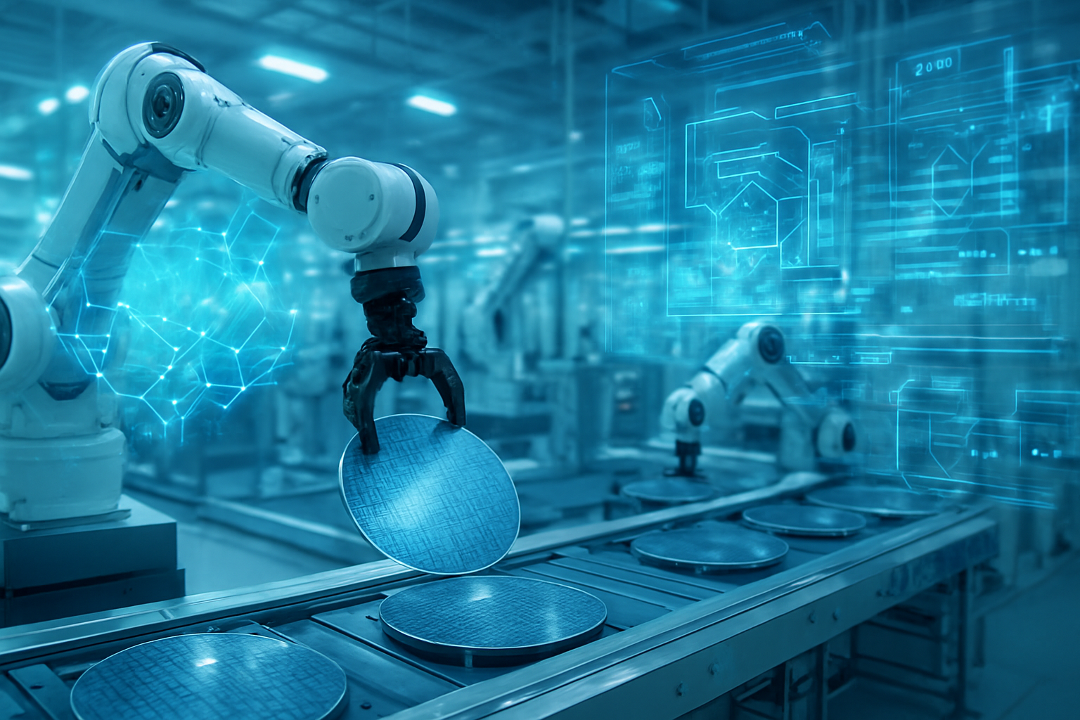
  • Veeco’s Lumina+ MOCVD System Ignites New Era for Compound Semiconductors, Fueling Next-Gen AI Hardware

    Veeco’s Lumina+ MOCVD System Ignites New Era for Compound Semiconductors, Fueling Next-Gen AI Hardware

    Veeco Instruments Inc. (NASDAQ: VECO) has unveiled its groundbreaking Lumina+ MOCVD System, a pivotal innovation poised to redefine the landscape of compound semiconductor manufacturing. This advanced Metal-Organic Chemical Vapor Deposition platform is not merely an incremental upgrade; it represents a significant leap forward in enabling the high-volume, cost-effective production of the specialized chips essential for the burgeoning demands of artificial intelligence. By enhancing throughput, uniformity, and wafer size capabilities, the Lumina+ system is set to become a cornerstone in the development of faster, more efficient, and increasingly powerful AI hardware, accelerating the pace of innovation across the entire tech industry.

    The immediate significance of the Lumina+ lies in its ability to address critical bottlenecks in the production of compound semiconductors—materials that offer superior electronic and optical properties compared to traditional silicon. As AI models grow in complexity and data processing requirements skyrocket, the need for high-performance components like VCSELs, edge-emitting lasers, and advanced LEDs becomes paramount. Veeco's new system promises to scale the manufacturing of these components, driving down costs and making advanced AI hardware more accessible for a wider range of applications, from autonomous vehicles to advanced data centers and immersive AR/VR experiences.

    Technical Prowess: Unpacking the Lumina+ Advancements

    The Lumina+ MOCVD System distinguishes itself through a suite of technological advancements designed for unparalleled performance and efficiency in compound semiconductor deposition. At its core, the system boasts the industry's largest arsenic phosphide (As/P) batch size, a critical factor for manufacturers aiming to reduce per-wafer costs and significantly boost overall output. This capacity, combined with best-in-class throughput, positions the Lumina+ as a leading solution for high-volume production, directly translating to a lower cost per wafer—a key metric for economic viability in advanced manufacturing.

    A cornerstone of Veeco's (NASDAQ: VECO) MOCVD technology is its proprietary TurboDisc® technology, which the Lumina+ seamlessly integrates and enhances. This proven reactor design is renowned for delivering exceptional thickness and compositional uniformity, low defectivity, and high yield over extended production campaigns. The TurboDisc® system employs a high-speed vertical rotating disk reactor and a sophisticated gas-distribution showerhead, creating optimal boundary layer conditions that minimize particle formation and contamination. This meticulous control is crucial for producing the high-precision epitaxial layers required for cutting-edge optoelectronic devices.

    A significant upgrade from its predecessor, the original Lumina platform which supported up to six-inch wafers, the Lumina+ now enables the deposition of high-quality As/P epitaxial layers on wafers up to eight inches in diameter. This seamless transition to larger wafer sizes without compromising process conditions, film uniformity, or composition is a game-changer for scaling production and achieving greater economies of scale. Furthermore, the system incorporates advanced process control mechanisms, including Veeco's Piezocon® gas concentration sensor, ensuring precise control of metal-organic flux. This level of precision is indispensable for manufacturing complex photonic integrated circuits (PICs) and microLED chips, guaranteeing identical deposition conditions across multiple MOCVD systems and enhancing overall product consistency.

    Initial reactions from the AI research community and industry experts highlight the Lumina+'s potential to accelerate foundational AI research by providing access to more advanced and cost-effective hardware. Compared to previous MOCVD systems, which often struggled with the balance between high throughput and stringent uniformity requirements for larger wafers, the Lumina+ offers a comprehensive solution. Its ability to achieve over 300 runs between chamber cleans also translates into system uptime exceeding 95%, a stark improvement that directly impacts production efficiency and operational costs, setting a new benchmark for MOCVD technology.

    Impact on the AI Ecosystem: Beneficiaries and Competitive Shifts

    The introduction of Veeco's (NASDAQ: VECO) Lumina+ MOCVD System is poised to send ripples throughout the artificial intelligence ecosystem, creating significant advantages for a diverse range of companies, from established tech giants to agile startups. Companies heavily invested in the development and deployment of next-generation AI hardware stand to benefit most directly. This includes firms specializing in optical communications, 3D sensing, LiDAR, augmented and virtual reality (AR/VR), and high-efficiency power electronics—all sectors where compound semiconductors are critical enablers.

    For major AI labs and tech companies like NVIDIA (NASDAQ: NVDA), Google (NASDAQ: GOOGL), Microsoft (NASDAQ: MSFT), and Amazon (NASDAQ: AMZN), which are constantly pushing the boundaries of AI model size and computational demands, the Lumina+ offers a pathway to more powerful and energy-efficient AI accelerators. The system's ability to produce high-quality VCSELs and edge-emitting lasers at scale will directly impact the performance of optical interconnects within data centers and between AI chips, reducing latency and increasing bandwidth—critical for distributed AI training and inference. Furthermore, the enhanced production capabilities for advanced displays (mini/microLEDs) will fuel innovation in human-machine interfaces for AI, particularly in AR/VR applications where visual fidelity and efficiency are paramount.

    The competitive implications are substantial. Manufacturers who adopt the Lumina+ early will gain a strategic advantage in cost-effectively scaling their production of compound semiconductor components. This could lead to a disruption in existing supply chains, as companies capable of producing these specialized chips at lower costs and higher volumes become preferred partners. For instance, Rocket Lab (NASDAQ: RKLB), a global leader in launch services and space systems, has already placed a multi-tool order for the Lumina+ system, leveraging it to double their production capacity for critical components like space-grade solar cells under the Department of Commerce’s CHIPS and Science Act initiatives. This demonstrates the immediate market positioning and strategic advantages conferred by the Lumina+ in enabling domestic production and enhancing national technological resilience.

    Startups focused on novel AI hardware architectures or specialized sensing solutions could also find new opportunities. The lowered cost per wafer and increased production efficiency might make previously unfeasible hardware designs economically viable, fostering a new wave of innovation. The Lumina+ essentially democratizes access to advanced compound semiconductor manufacturing, enabling a broader array of companies to integrate high-performance optoelectronic components into their AI products and services, thereby accelerating the overall pace of AI development and deployment.

    Wider Significance: Reshaping the AI Landscape

    The advent of Veeco's (NASDAQ: VECO) Lumina+ MOCVD System represents more than just a technological upgrade; it signifies a pivotal moment in the broader AI landscape, aligning perfectly with the escalating demand for specialized, high-performance computing. As AI models become increasingly sophisticated and data-intensive, the limitations of traditional silicon-based architectures are becoming apparent. Compound semiconductors, with their inherent advantages in speed, energy efficiency, and optical properties, are emerging as the fundamental building blocks for next-generation AI, and the Lumina+ is the engine driving their mass production.

    This development fits squarely into the overarching trend of hardware-software co-design in AI, where advancements in physical components directly enable breakthroughs in algorithmic capabilities. By making high-quality VCSELs for 3D sensing, LiDAR, and high-speed data communication more accessible and affordable, the Lumina+ will accelerate the development of autonomous systems, robotics, and advanced perception technologies that rely heavily on rapid and accurate environmental understanding. Similarly, its role in producing edge-emitting lasers for advanced optical communications and silicon photonics will underpin the high-bandwidth, low-latency interconnects crucial for hyperscale AI data centers and distributed AI inference networks.

    The impacts extend beyond mere performance gains. The Lumina+ contributes to greater energy efficiency in AI hardware, a growing concern given the massive power consumption of large AI models. Compound semiconductors often operate with less power and generate less heat than silicon, leading to more sustainable and cost-effective AI operations. However, potential concerns include the complexity of MOCVD processes and the need for highly skilled operators, which could pose a challenge for widespread adoption without adequate training and infrastructure. Nonetheless, the system's high uptime and advanced process control aim to mitigate some of these operational complexities.

    Comparing this to previous AI milestones, the Lumina+ can be seen as an enabler akin to the development of advanced GPUs in the early 2010s, which unlocked the deep learning revolution. While not a direct AI algorithm breakthrough, it is a foundational manufacturing innovation that will indirectly fuel countless AI advancements by providing the necessary hardware infrastructure. It underpins the shift towards photonics and advanced materials in computing, moving AI beyond the confines of purely electronic processing and into an era where light plays an increasingly critical role in data handling.

    Future Developments: The Road Ahead for AI Hardware

    Looking ahead, the Veeco (NASDAQ: VECO) Lumina+ MOCVD System is poised to be a catalyst for several near-term and long-term developments in AI hardware. In the near term, we can expect a surge in the availability and affordability of high-performance compound semiconductor components. This will directly translate into more powerful and efficient AI accelerators, improved sensors for autonomous systems, and higher-resolution, more energy-efficient displays for AR/VR applications. Companies currently limited by the cost or scalability of these components will find new avenues for product innovation and market expansion.

    On the horizon, the long-term implications are even more profound. The Lumina+ paves the way for advanced photonic integrated circuits (PICs) to become a standard in AI computing, potentially leading to entirely new architectures where light-based communication and computation minimize energy loss and maximize speed. This could enable true optical AI processors, a significant leap beyond current electronic designs. Furthermore, the ability to produce high-quality mini and microLEDs at scale will accelerate the development of truly immersive and interactive AI experiences, where seamless visual feedback is critical.

    However, several challenges need to be addressed to fully realize the potential of these developments. Continued research into novel compound semiconductor materials and deposition techniques will be crucial to push performance boundaries even further. The integration of these advanced components into complex AI systems will also require sophisticated packaging and interconnect technologies. Additionally, the industry will need to cultivate a skilled workforce capable of operating and maintaining these advanced MOCVD systems and designing with these new materials.

    Experts predict that the Lumina+'s impact will be felt across various sectors, from quantum computing, where precise material control is paramount, to advanced medical imaging and biotechnology, which can leverage high-performance optoelectronic devices. The system's emphasis on scalability and cost-effectiveness suggests a future where advanced AI hardware is not a niche luxury but a widespread commodity, driving innovation across the entire technological spectrum. We can anticipate further optimization of MOCVD processes, potentially leading to even larger wafer sizes and more complex multi-layer structures, continuously pushing the envelope of what's possible in AI hardware.

    Wrap-up: A New Dawn for AI's Foundation

    In summary, Veeco's (NASDAQ: VECO) Lumina+ MOCVD System marks a definitive inflection point in the manufacturing of compound semiconductors, laying a crucial foundation for the next generation of artificial intelligence hardware. The system's unparalleled features—including the largest As/P batch size, best-in-class throughput, lowest cost per wafer, and support for eight-inch wafers—represent significant technological leaps. These advancements, built upon the proven TurboDisc® technology and enhanced with precise process control, directly address the escalating demand for high-performance, energy-efficient components vital for complex AI applications.

    This development's significance in AI history cannot be overstated; it is a critical enabler that will accelerate the transition from silicon-centric AI hardware to more advanced compound semiconductor and photonic-based solutions. By making the production of components like VCSELs, edge-emitting lasers, and advanced LEDs more scalable and cost-effective, the Lumina+ is poised to democratize access to cutting-edge AI capabilities, fostering innovation across startups, tech giants, and specialized hardware developers alike. Its impact will be seen in faster AI models, more intelligent autonomous systems, and more immersive AR/VR experiences.

    The long-term impact of the Lumina+ extends to shaping the very architecture of future computing, moving towards a paradigm where light plays an increasingly central role in processing and communication. While challenges related to material science and integration remain, the trajectory set by Veeco's innovation is clear: a future where AI hardware is not just more powerful, but also more efficient, sustainable, and capable of addressing the most complex challenges facing humanity.

    In the coming weeks and months, industry watchers should keenly observe the adoption rate of the Lumina+ system across the compound semiconductor manufacturing landscape. Key indicators will include new customer announcements, production ramp-ups from early adopters like Rocket Lab (NASDAQ: RKLB), and the subsequent unveiling of AI hardware products leveraging these newly scalable components. The ripple effects of this foundational manufacturing breakthrough will undoubtedly redefine the competitive landscape and accelerate the evolution of AI as we know it.

    This content is intended for informational purposes only and represents analysis of current AI developments.

    TokenRing AI delivers enterprise-grade solutions for multi-agent AI workflow orchestration, AI-powered development tools, and seamless remote collaboration platforms.
    For more information, visit https://www.tokenring.ai/.

  • Google’s $4 Billion Arkansas Bet: Fueling the Future of U.S. AI Innovation

    Google’s $4 Billion Arkansas Bet: Fueling the Future of U.S. AI Innovation

    Google (NASDAQ: GOOGL) has announced a monumental $4 billion investment in cloud and artificial intelligence (AI) infrastructure in Arkansas through 2027, marking a significant stride in the tech giant's commitment to advancing U.S. AI capabilities. This substantial financial injection will primarily fund the construction of Google's first data center in the state, located in West Memphis, and underscores a strategic push to expand the company's regional cloud presence and enhance its AI processing power. The announcement, made on October 2, 2025, with further elaborations by Google and Alphabet CEO Sundar Pichai on October 6, 2025, highlights Arkansas's emerging role in the national AI landscape.

    This multi-faceted investment is poised to have immediate and far-reaching implications for AI innovation across the United States. By establishing a new, massive data center and integrating sustainable energy solutions, Google is not only scaling its operational capacity but also setting a precedent for responsible AI development. The initiative is expected to generate thousands of jobs, foster a skilled workforce through free AI training programs, and solidify the U.S.'s competitive edge in the global AI race, demonstrating Google's dedication to both technological advancement and regional economic growth.

    The Technical Core of Google's Arkansas Expansion

    Google's $4 billion investment is anchored by the development of its first Arkansas data center, an expansive facility spanning over 1,000 acres in West Memphis. This new infrastructure is meticulously designed to serve as a critical hub for cloud and AI operations, providing the colossal computing power necessary to train sophisticated large language models and process the ever-growing datasets that fuel advanced AI applications. The scale of this data center signifies a substantial increase in Google's capacity to handle the surging demand for AI computing, offering enhanced reliability and speed for businesses relying on AI-powered cloud services, particularly in the Southern U.S.

    Beyond the physical data center, Google is integrating cutting-edge energy initiatives to power its operations sustainably. A $25 million Energy Impact Fund will support energy efficiency and affordability for local residents, while a collaboration with Entergy will bring a new 600 MW solar project to the grid, complemented by a 350 MW battery storage system. This commitment to renewable energy and grid stability differentiates Google's approach, demonstrating an effort to mitigate the significant energy demands typically associated with large-scale AI infrastructure. This sustainable design is a crucial evolution from previous data center models, which often faced criticism for their environmental footprint, positioning Google as a leader in eco-conscious AI development.

    Initial reactions from the AI research community and industry experts have been overwhelmingly positive. Many see this investment as a vital step in strengthening the foundational infrastructure required for the next generation of AI breakthroughs. The emphasis on both raw processing power and sustainable energy has been particularly lauded, indicating a maturing understanding within the industry of the broader societal and environmental responsibilities that come with scaling AI technologies. Experts predict that this robust infrastructure will accelerate research and development in areas like generative AI, advanced machine learning, and autonomous systems.

    Competitive Implications and Market Positioning

    This significant investment by Google (NASDAQ: GOOGL) in Arkansas carries profound implications for the competitive landscape of the AI sector, impacting tech giants, emerging AI labs, and startups alike. Google's expansion of its cloud and AI infrastructure directly strengthens its competitive position against rivals such as Amazon (NASDAQ: AMZN) with Amazon Web Services (AWS) and Microsoft (NASDAQ: MSFT) with Azure, both of whom are also heavily investing in AI-driven cloud solutions. By increasing its data center footprint and processing capabilities, Google can offer more robust, faster, and potentially more cost-effective AI services, attracting a broader array of enterprise clients and developers.

    Companies heavily reliant on Google Cloud for their AI workloads stand to benefit immensely from this development. Startups and mid-sized businesses leveraging Google's AI Platform or various AI/ML APIs will experience enhanced performance, reduced latency, and greater scalability, which are critical for deploying and iterating on AI-powered products and services. This investment could also encourage new startups to build on Google Cloud, given the enhanced infrastructure and the company's commitment to fostering a skilled workforce through its training programs.

    The strategic advantage for Google lies in its ability to further integrate its AI research directly into its cloud offerings. This tight coupling allows for faster deployment of new AI models and features, potentially disrupting existing products or services offered by competitors who may not have the same level of integrated hardware and software development. Furthermore, the focus on sustainable energy solutions could become a key differentiator, appealing to environmentally conscious businesses and governmental organizations. This move solidifies Google's market positioning as not just a leader in AI research, but also as a provider of the foundational infrastructure essential for the widespread adoption and development of AI.

    Broader Significance in the AI Landscape

    Google's $4 billion investment in Arkansas is a pivotal development that seamlessly integrates into the broader AI landscape and reflects several overarching trends. Firstly, it underscores the escalating demand for computational power driven by the rapid advancements in AI, particularly in large language models and complex machine learning algorithms. This investment signifies that the "AI race" is not just about algorithmic innovation, but also about the physical infrastructure required to support it. It aligns with a global trend of major tech players establishing regional data centers to bring AI closer to users and developers, thereby reducing latency and improving service delivery.

    The impacts of this investment extend beyond mere technological expansion. Economically, it promises to revitalize the local Arkansas economy, creating thousands of construction jobs and hundreds of high-skilled operational roles. The provision of free AI courses and certifications, in partnership with the Arkansas Department of Commerce, is a critical initiative aimed at upskilling the local workforce, creating a talent pipeline that will support not only Google's operations but also foster a broader tech ecosystem in the region. This human capital development is crucial for ensuring equitable access to the opportunities presented by the AI revolution.

    While the benefits are substantial, potential concerns could include the environmental impact of such a large-scale data center, even with Google's commitment to renewable energy. The sheer volume of resources required for construction and ongoing operation necessitates careful monitoring. Comparisons to previous AI milestones, such as the initial breakthroughs in deep learning or the widespread adoption of cloud computing, highlight that infrastructure investments of this magnitude are often precursors to significant leaps in technological capability and accessibility. This move by Google is reminiscent of the foundational investments made during the early days of the internet, laying the groundwork for future innovation.

    Future Developments and Expert Predictions

    Looking ahead, Google's substantial investment in Arkansas is expected to catalyze a wave of near-term and long-term developments in the U.S. AI landscape. In the near term, we can anticipate a rapid acceleration in the construction phase of the West Memphis data center, leading to the creation of thousands of construction jobs and a significant boost to local economies. Once operational, the data center will provide a powerful new hub for Google Cloud services, attracting businesses and developers seeking high-performance AI and cloud computing resources, particularly in the Southern U.S.

    In the long term, this infrastructure is poised to unlock a plethora of potential applications and use cases. Enhanced processing power and reduced latency will facilitate the development and deployment of more sophisticated AI models, including advanced generative AI, real-time analytics, and highly complex simulations across various industries. We can expect to see advancements in areas such as precision agriculture, logistics optimization, and personalized healthcare, all powered by the increased AI capabilities. The workforce development initiatives, offering free AI courses and certifications, will also contribute to a more AI-literate population, potentially fostering a new generation of AI innovators and entrepreneurs in Arkansas and beyond.

    However, challenges remain. The continuous demand for energy to power such large-scale AI infrastructure will necessitate ongoing innovation in renewable energy and energy efficiency. Cybersecurity will also be paramount, as these data centers become critical national assets. Experts predict that this investment will solidify Google's position as a dominant player in the AI infrastructure space, potentially leading to further regional investments by other tech giants as they seek to compete. The expectation is that this will foster a more distributed and resilient AI infrastructure across the U.S., ultimately accelerating the pace of AI innovation and its integration into daily life.

    A New Era for U.S. AI Infrastructure

    Google's (NASDAQ: GOOGL) $4 billion investment in Arkansas represents a pivotal moment in the ongoing evolution of artificial intelligence and cloud computing infrastructure in the United States. The construction of a new, state-of-the-art data center in West Memphis, coupled with significant commitments to sustainable energy and workforce development, underscores a strategic vision that extends beyond mere technological expansion. Key takeaways include the substantial boost to U.S. AI processing capabilities, the creation of thousands of jobs, and the establishment of a new regional hub for AI innovation, particularly in the Southern U.S.

    This development holds immense significance in AI history, marking a new chapter where the physical infrastructure supporting AI becomes as critical as the algorithmic breakthroughs themselves. It signifies a move towards a more robust, distributed, and sustainable AI ecosystem, addressing the growing demands for computational power while also acknowledging environmental responsibilities. The investment in human capital through free AI training programs is equally important, ensuring that the benefits of this technological advancement are accessible to a broader segment of the population.

    In the coming weeks and months, industry observers will be closely watching the progress of the data center's construction and the impact of Google's workforce development initiatives. We can expect further announcements regarding partnerships, new AI services leveraging this enhanced infrastructure, and potentially, similar investments from competing tech giants. This monumental undertaking by Google is not just an investment in technology; it is an investment in the future of U.S. AI leadership and a testament to the transformative power of artificial intelligence.

    This content is intended for informational purposes only and represents analysis of current AI developments.

    TokenRing AI delivers enterprise-grade solutions for multi-agent AI workflow orchestration, AI-powered development tools, and seamless remote collaboration platforms.
    For more information, visit https://www.tokenring.ai/.

  • Meta Eyes Rivos Acquisition: A Bold Leap Towards AI Silicon Independence and Nvidia Decoupling

    Meta Eyes Rivos Acquisition: A Bold Leap Towards AI Silicon Independence and Nvidia Decoupling

    In a move poised to reshape the landscape of artificial intelligence hardware, Meta Platforms (NASDAQ: META) is reportedly in advanced discussions to acquire Rivos, a promising AI chip startup. Emerging just days ago, around September 30, 2025, these rumors, initially reported by Bloomberg News and subsequently corroborated by other tech outlets, signal a pivotal moment for the social media giant. This potential acquisition is not merely about expanding Meta's portfolio; it represents a strategic, aggressive push to bolster its internal AI silicon program, significantly reduce its multi-billion-dollar reliance on Nvidia (NASDAQ: NVDA) GPUs, and gain tighter control over its burgeoning AI infrastructure. The implications of such a deal could reverberate across the tech industry, intensifying the race for AI hardware supremacy.

    Meta's reported frustrations with the pace of its own Meta Training and Inference Accelerator (MTIA) chip development have fueled this pursuit. CEO Mark Zuckerberg is said to be keen on accelerating the company's capabilities in custom silicon, viewing it as critical to powering everything from its vast social media algorithms to its ambitious metaverse projects. By integrating Rivos's expertise and technology, Meta aims to fast-track its journey towards AI hardware independence, optimize performance for its unique workloads, and ultimately achieve substantial long-term cost savings.

    The Technical Core: Rivos's RISC-V Prowess Meets Meta's MTIA Ambitions

    The heart of Meta's interest in Rivos lies in the startup's specialized expertise in designing GPUs and AI accelerators built upon the open-source RISC-V instruction set architecture. Unlike proprietary architectures from companies like Arm, Intel (NASDAQ: INTC), or AMD (NASDAQ: AMD), RISC-V offers unparalleled flexibility, customization, and potentially lower licensing costs, making it an attractive foundation for companies seeking to build highly tailored silicon. Rivos has reportedly focused on developing full-stack AI systems around this architecture, providing not just chip designs but also the necessary software and tools to leverage them effectively.

    This technical alignment is crucial for Meta's ongoing MTIA project. The MTIA chips, which Meta has been developing in-house, reportedly in collaboration with Broadcom (NASDAQ: AVGO), are also believed to be based on the RISC-V standard. While MTIA chips have seen limited deployment within Meta's data centers, operating in tandem with Nvidia GPUs, the integration of Rivos's advanced RISC-V designs and engineering talent could provide a significant accelerant. It could enable Meta to rapidly iterate on its MTIA designs, enhancing their performance, efficiency, and scalability for tasks ranging from content ranking and recommendation engines to advanced AI model training. This move signals a deeper commitment to a modular, open-source approach to hardware, potentially diverging from the more closed ecosystems of traditional chip manufacturers.

    The acquisition would allow Meta to differentiate its AI hardware strategy from existing technologies, particularly those offered by Nvidia. While Nvidia's CUDA platform and powerful GPUs remain the industry standard for AI training, Meta's tailored RISC-V-based MTIA chips, enhanced by Rivos, could offer superior performance-per-watt and cost-effectiveness for its specific, massive-scale inference and potentially even training workloads. This is not about outright replacing Nvidia overnight, but about building a complementary, highly optimized internal infrastructure that reduces dependency and provides strategic leverage. The industry is closely watching to see how this potential synergy will manifest in Meta's next generation of data centers, where custom silicon could redefine the balance of power.

    Reshaping the AI Hardware Battleground

    Should the acquisition materialize, Meta Platforms stands to be the primary beneficiary. The influx of Rivos's specialized talent and intellectual property would significantly de-risk and accelerate Meta's multi-year effort to develop its own custom AI silicon. This would translate into greater control over its technology stack, improved operational efficiency, and potentially billions in cost savings by reducing its reliance on costly third-party GPUs. Furthermore, having purpose-built chips could give Meta a competitive edge in deploying cutting-edge AI features faster and more efficiently across its vast ecosystem, from Instagram to the metaverse.

    For Nvidia, the implications are significant, though not immediately catastrophic. Meta is one of Nvidia's largest customers, spending billions annually on its GPUs. While Meta's "dual-track approach"—continuing to invest in Nvidia platforms for immediate needs while building its own chips for long-term independence—suggests a gradual shift, a successful Rivos integration would undeniably reduce Nvidia's market share within Meta's infrastructure over time. This intensifies the competitive pressure on Nvidia, pushing it to innovate further and potentially explore new market segments or deeper partnerships with other hyperscalers. The move underscores a broader trend among tech giants to internalize chip development, a challenge Nvidia has been proactively addressing by diversifying its offerings and software ecosystem.

    The ripple effect extends to other tech giants and chip startups. Companies like Google (NASDAQ: GOOGL), Amazon (NASDAQ: AMZN), and Microsoft (NASDAQ: MSFT) have already invested heavily in their own custom AI chips (TPUs, Inferentia/Trainium, Maia/Athena respectively). Meta's potential Rivos acquisition signals an escalation in this "in-house silicon" arms race, validating the strategic importance of custom hardware for AI leadership. For smaller chip startups, this could be a mixed bag: while Rivos's acquisition highlights the value of specialized AI silicon expertise, it also means one less independent player in the ecosystem, potentially leading to increased consolidation. The market positioning of companies like Cerebras Systems or Graphcore, which offer alternative AI accelerators, might also be indirectly affected as hyperscalers increasingly build their own solutions.

    The Broader AI Canvas: Independence, Innovation, and Concerns

    Meta's potential acquisition of Rivos fits squarely into a broader and accelerating trend within the AI landscape: the strategic imperative for major tech companies to develop their own custom silicon. This shift is driven by the insatiable demand for AI compute, the limitations of general-purpose GPUs for highly specific workloads, and the desire for greater control over performance, cost, and supply chains. It represents a maturation of the AI industry, where hardware innovation is becoming as critical as algorithmic breakthroughs. The move could foster greater innovation in chip design, particularly within the open-source RISC-V ecosystem, as more resources are poured into developing tailored solutions for diverse AI applications.

    However, this trend also raises potential concerns. The increasing vertical integration by tech giants could lead to a more fragmented hardware landscape, where specialized chips are optimized for specific ecosystems, potentially hindering interoperability and the broader adoption of universal AI development tools. There's also a risk of talent drain from the broader semiconductor industry into these massive tech companies, concentrating expertise and potentially limiting the growth of independent chip innovators. Comparisons to previous AI milestones, such as the rise of deep learning or the proliferation of cloud AI services, highlight that foundational hardware shifts often precede significant advancements in AI capabilities and applications.

    The impacts extend beyond just performance and cost. Greater independence in silicon development can offer significant geopolitical advantages, reducing reliance on external supply chains and enabling more resilient infrastructure. It also allows Meta to tightly integrate hardware and software, potentially unlocking new efficiencies and capabilities that are difficult to achieve with off-the-shelf components. The adoption of RISC-V, in particular, could democratize chip design in the long run, offering an alternative to proprietary architectures and fostering a more open hardware ecosystem, even as large players like Meta leverage it for their own strategic gain.

    Charting the Future of Meta's AI Silicon Journey

    In the near term, the integration of Rivos's team and technology into Meta's AI division will be paramount. We can expect an acceleration in the development and deployment of next-generation MTIA chips, potentially leading to more widespread use within Meta's data centers for both inference and, eventually, training workloads. The collaboration could yield more powerful and efficient custom accelerators tailored for Meta's specific needs, such as powering the complex simulations of the metaverse, enhancing content moderation, or refining recommendation algorithms across its social platforms.

    Longer term, this acquisition positions Meta to become a formidable player in AI hardware, potentially challenging Nvidia's dominance in specific segments. The continuous refinement of custom silicon could lead to entirely new classes of AI applications and use cases that are currently cost-prohibitive or technically challenging with general-purpose hardware. Challenges that need to be addressed include the complexities of integrating Rivos's technology and culture, scaling up production of custom chips, and building a robust software ecosystem around the new hardware to ensure developer adoption and ease of use. Experts predict that other hyperscalers will likely double down on their own custom silicon efforts, intensifying the competition and driving further innovation in the AI chip space. The era of generic hardware for every AI task is rapidly fading, replaced by a specialized, purpose-built approach.

    A New Era of AI Hardware Autonomy Dawns

    Meta's reported exploration of acquiring Rivos marks a significant inflection point in its strategic pursuit of AI autonomy. The key takeaway is clear: major tech companies are no longer content to be mere consumers of AI hardware; they are becoming active architects of their own silicon destiny. This move underscores Meta's deep commitment to controlling its technological stack, reducing financial and supply chain dependencies on external vendors like Nvidia, and accelerating its AI ambitions across its diverse product portfolio, from social media to the metaverse.

    This development is likely to be remembered as a critical moment in AI history, symbolizing the shift towards vertical integration in the AI industry. It highlights the growing importance of custom silicon as a competitive differentiator and a foundational element for future AI breakthroughs. The long-term impact will likely see a more diversified and specialized AI hardware market, with hyperscalers driving innovation in purpose-built chips, potentially leading to more efficient, powerful, and cost-effective AI systems.

    In the coming weeks and months, the industry will be watching for official announcements regarding the Rivos acquisition, details on the integration strategy, and early benchmarks of Meta's accelerated MTIA program. The implications for Nvidia, the broader semiconductor market, and the trajectory of AI innovation will be a central theme in tech news, signaling a new era where hardware independence is paramount for AI leadership.

    This content is intended for informational purposes only and represents analysis of current AI developments.
    TokenRing AI delivers enterprise-grade solutions for multi-agent AI workflow orchestration, AI-powered development tools, and seamless remote collaboration platforms.
    For more information, visit https://www.tokenring.ai/.