Blog

  • SK Hynix Unleashes $14.6 Billion Chip Plant in South Korea, Igniting the AI Memory Supercycle

    SK Hynix Unleashes $14.6 Billion Chip Plant in South Korea, Igniting the AI Memory Supercycle

    SK Hynix (KRX: 000660), a global leader in memory semiconductors, has announced a monumental investment of over 20 trillion Korean won (approximately $14.6 billion USD) to construct a new, state-of-the-art chip manufacturing facility in Cheongju, South Korea. Announced on April 24, 2024, this massive capital injection is primarily aimed at dramatically boosting the production of High Bandwidth Memory (HBM) and other advanced artificial intelligence (AI) chips. With construction slated for completion by November 2025, this strategic move is set to reshape the landscape of memory chip production, address critical global supply shortages, and intensify the competitive dynamics within the rapidly expanding semiconductor industry.

    The investment underscores SK Hynix's aggressive strategy to solidify its "unrivaled technological leadership" in the burgeoning AI memory sector. As AI applications, particularly large language models (LLMs) and generative AI, continue their explosive growth, the demand for high-performance memory has outstripped supply, creating a critical bottleneck. SK Hynix's new facility is a direct response to this "AI supercycle," positioning the company to meet the insatiable appetite for the specialized memory crucial to power the next generation of AI innovation.

    Technical Prowess and a Strategic Pivot Towards HBM Dominance

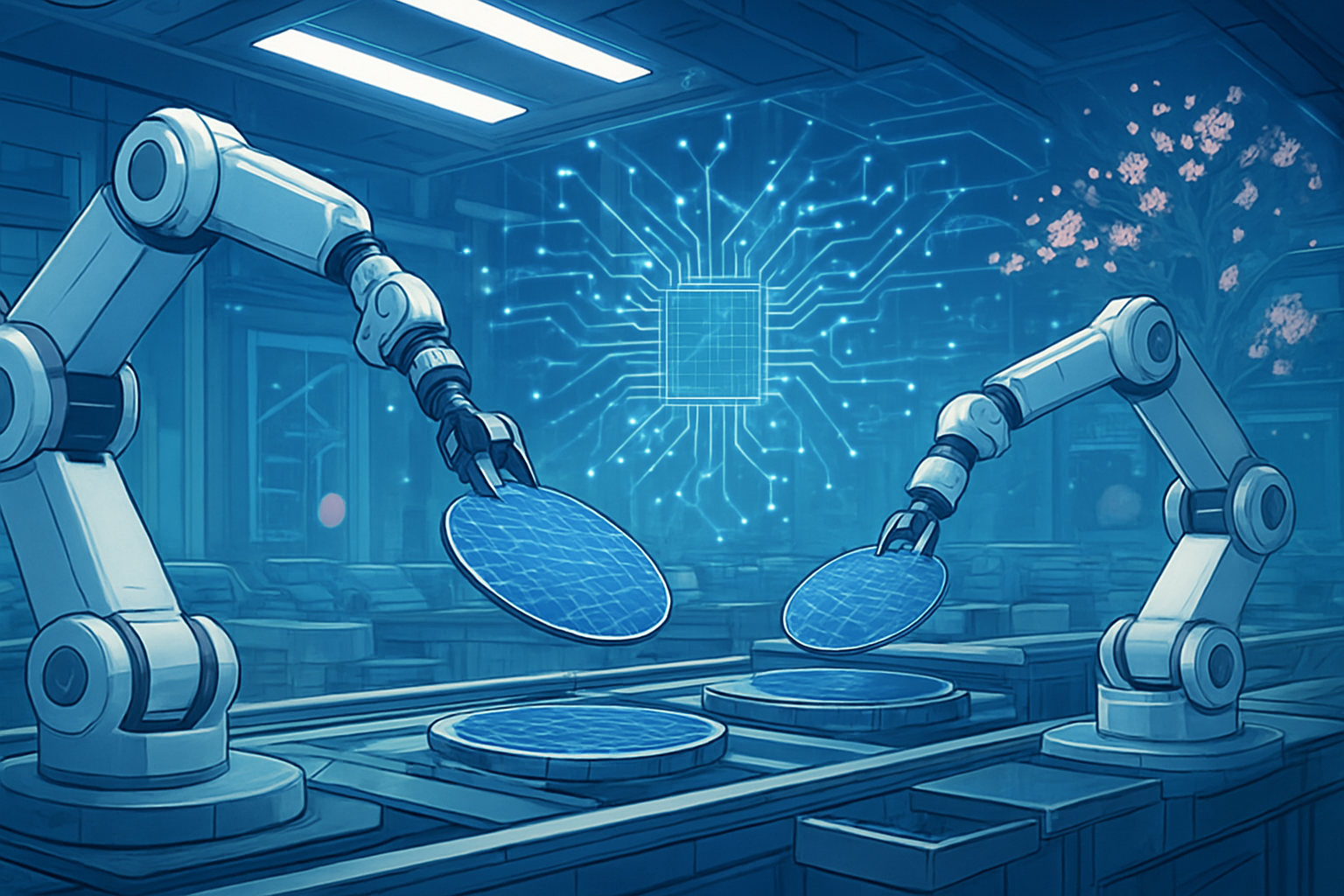
    The new M15X fab in Cheongju represents a significant technical leap and a strategic pivot for SK Hynix. Initially envisioned as a NAND flash production line, the company boldly redirected the investment, increasing its scope and dedicating the facility entirely to next-generation DRAM and HBM production. This reflects a rapid and decisive response to market dynamics, with a downturn in flash memory coinciding with an unprecedented surge in HBM demand.

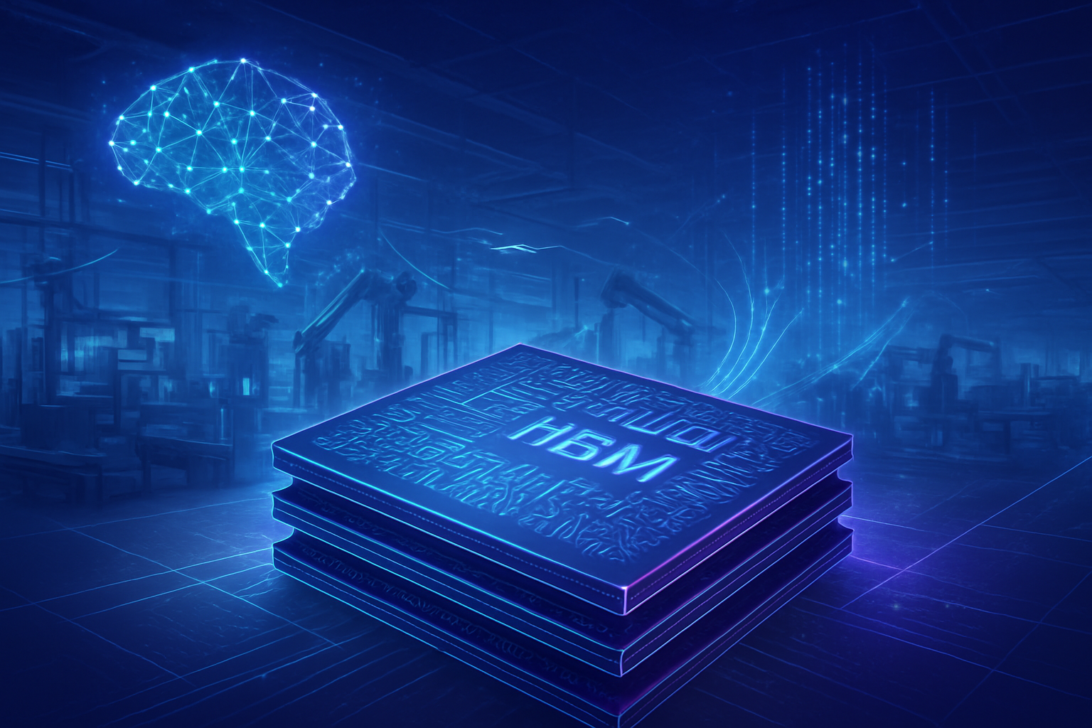
    The M15X facility is designed to be a new DRAM production base specifically focused on manufacturing cutting-edge HBM products, particularly those based on 1b DRAM, which forms the core chip for SK Hynix's HBM3E. The company has already achieved significant milestones, being the first to supply 8-layer HBM3E to NVIDIA (NASDAQ: NVDA) in March 2024 and commencing mass production of 12-layer HBM3E products in September 2024. Looking ahead, SK Hynix has provided samples of its HBM4 12H (36GB capacity, 2TB/s data rate) and is preparing for HBM4 mass production in 2026.

    Expected production capacity increases are substantial. While initial plans projected 32,000 wafers per month for 1b DRAM, SK Hynix is considering nearly doubling this, with a new target potentially reaching 55,000 to 60,000 wafers per month. Some reports even suggest a capacity of 100,000 sheets of 12-inch DRAM wafers monthly. By the end of 2026, with M15X fully operational, SK Hynix aims for a total 1b DRAM production capacity of 240,000 wafers per month across its fabs. This aggressive ramp-up is critical, as the company has already reported its HBM production capacity for 2025 is completely sold out.

    Advanced packaging technologies are at the heart of this investment. The M15X will leverage Through-Silicon Via (TSV) technology, essential for HBM's 3D-stacked architecture. For the upcoming HBM4 generation, SK Hynix plans a groundbreaking collaboration with Taiwan Semiconductor Manufacturing Company (TSMC) (NYSE: TSM) to adopt TSMC's advanced logic process for the HBM base die. This represents a new approach, moving beyond proprietary technology for the base die to enhance logic-HBM integration, allowing for greater functionality and customization in performance and power efficiency. The company is also constructing a new "Package & Test (P&T) 7" facility in Cheongju to further strengthen its advanced packaging capabilities, underscoring the increasing importance of back-end processes in semiconductor performance.

    Initial reactions from the AI research community and industry experts have been overwhelmingly positive, highlighting the persistent HBM supply shortage. NVIDIA CEO Jensen Huang has reportedly requested accelerated delivery schedules, even asking SK Hynix to expedite HBM4 supply by six months. Industry analysts believe SK Hynix's aggressive investment will alleviate concerns about advanced memory chip production capacity, crucial for maintaining its leadership in the HBM market, especially given its smaller overall DRAM production capacity compared to competitors.

    Reshaping the AI Industry: Beneficiaries and Competitive Dynamics

    SK Hynix's substantial investment in HBM production is poised to significantly reshape the artificial intelligence industry, benefiting key players while intensifying competition among memory manufacturers and AI hardware developers. The increased availability of HBM, crucial for its superior data transfer rates, energy efficiency, and low latency, will directly address a critical bottleneck in AI development and deployment.

    Which companies stand to benefit most?
    As the dominant player in AI accelerators, NVIDIA (NASDAQ: NVDA) is a primary beneficiary. SK Hynix is a major HBM supplier for NVIDIA's AI GPUs, and an expanded HBM supply ensures NVIDIA can continue to meet surging demand, potentially reducing supply constraints. Similarly, AMD (NASDAQ: AMD), with its Instinct MI300X and future GPUs, will gain from a more robust HBM supply to scale its AI offerings. Intel (NASDAQ: INTC), which integrates HBM into its high-performance Xeon Scalable processors and AI accelerators, will also benefit from increased production to support its integrated HBM solutions and open chiplet marketplace strategy. TSMC (NYSE: TSM), as the leading foundry and partner for HBM4, stands to benefit from the advanced packaging collaboration. Beyond these tech giants, numerous AI startups and cloud service providers operating large AI data centers will find relief in a more accessible HBM supply, potentially lowering costs and accelerating innovation.

    Competitive Implications:
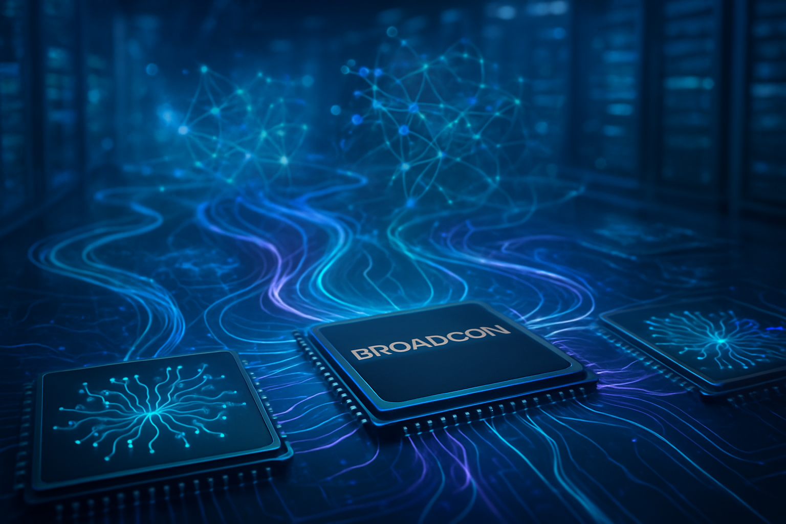
    The HBM market is a fiercely contested arena, primarily between SK Hynix, Samsung Electronics (KRX: 005930), and Micron Technology (NASDAQ: MU). SK Hynix's investment is a strategic move to cement its leadership, particularly in HBM3 and HBM3E, where it has held a significant market share and strong ties with NVIDIA. However, Samsung (KRX: 005930) is aggressively expanding its HBM capacity, reportedly surpassing SK Hynix in HBM production volume recently, and aims to become a major supplier for NVIDIA and other tech giants. Micron (NASDAQ: MU) is also rapidly ramping up its HBM3E production, securing design wins, and positioning itself as a strong contender in HBM4. This intensified competition among the three memory giants could lead to more stable pricing and accelerate the development of even more advanced HBM technologies.

    Potential Disruption and Market Positioning:
    The "supercycle" in HBM demand is already causing a reallocation of wafer capacity from traditional DRAM to HBM, leading to potential shortages and price surges in conventional DRAM (like DDR5) for consumer PCs and smartphones. For AI products, however, the increased HBM supply will likely prevent bottlenecks, enabling faster product cycles and more powerful iterations of AI hardware and software. In terms of market positioning, SK Hynix aims to maintain its "first-mover advantage," but aggressive strategies from Samsung and Micron suggest a dynamic shift in market share is expected. The ability to produce HBM4 at scale with high yields will be a critical determinant of future market leadership. AI hardware developers like NVIDIA will gain strategic advantages from a stable and technologically advanced HBM supply, enabling them to design more powerful AI accelerators.

    Wider Significance: Fueling the AI Revolution and Geopolitical Shifts

    SK Hynix's $14.6 billion investment in HBM production transcends mere corporate expansion; it represents a pivotal moment in the broader AI landscape and global semiconductor trends. HBM is unequivocally a "foundational enabler" of the current "AI supercycle," directly addressing the "memory wall" bottleneck that has traditionally hampered the performance of advanced processors. Its 3D-stacked architecture, offering unparalleled bandwidth, lower latency, and superior power efficiency, is indispensable for training and inferencing complex AI models like LLMs, which demand immense computational power and rapid data processing.

    This investment reinforces HBM's central role as the backbone of the AI economy. SK Hynix, a pioneer in HBM technology since its first development in 2013, has consistently driven advancements through successive generations. Its primary supplier status for NVIDIA's AI GPUs and dominant market share in HBM3 and HBM3E highlight how specialized memory has evolved from a commodity to a high-value, strategic component.

    Global Semiconductor Trends: Chip Independence and Supply Chain Resilience
    The strategic implications extend to global semiconductor trends, particularly chip independence and supply chain resilience. SK Hynix's broader strategy includes establishing a $3.9 billion advanced packaging plant in Indiana, U.S., slated for HBM mass production by the second half of 2028. This move aligns with the U.S. "reshoring" agenda, aiming to reduce reliance on concentrated supply chains and secure access to government incentives like the CHIPS Act. Such geographical diversification enhances the resilience of the global semiconductor supply chain by spreading production capabilities, mitigating risks associated with localized disruptions. South Korea's own "K-Semiconductor Strategy" further emphasizes this dual approach towards national self-sufficiency and reduced dependency on single points of failure.

    Geopolitical Considerations:
    The investment unfolds amidst intensifying geopolitical competition, notably the US-China tech rivalry. While U.S. export controls have impacted some rivals, SK Hynix's focus on HBM for AI allows it to navigate these challenges, with the Indiana plant aligning with U.S. geopolitical priorities. The industry is witnessing a "bifurcation," where SK Hynix and Samsung dominate the global market for high-end HBM, while Chinese manufacturers like CXMT are rapidly advancing to supply China's burgeoning AI sector, albeit still lagging due to technology restrictions. This creates a fragmented market where geopolitical alliances increasingly dictate supplier choices and supply chain configurations.

    Potential Concerns:
    Despite the optimistic outlook, concerns exist regarding a potential HBM oversupply and subsequent price drops starting in 2026, as competitors ramp up their production capacities. Goldman Sachs, for example, forecasts a possible double-digit drop in HBM prices. However, SK Hynix dismisses these concerns, asserting that demand will continue to outpace supply through 2025 due to technological challenges in HBM production and ever-increasing computing power requirements for AI. The company projects the HBM market to expand by 30% annually until 2030.

    Environmental impact is another growing concern. The increasing die stacks within HBM, potentially reaching 24 dies per stack, lead to higher carbon emissions due to increased silicon volume. The adoption of Extreme Ultraviolet (EUV) lithography for advanced DRAM also contributes to Scope 2 emissions from electricity consumption. However, advancements in memory density and yield-improving technologies can help mitigate these impacts.

    Comparisons to Previous AI Milestones:
    SK Hynix's HBM investment is comparable in significance to other foundational breakthroughs in AI's history. HBM itself is considered a "pivotal moment" that directly contributed to the explosion of LLMs. Its introduction in 2013, initially an "overlooked piece of hardware," became a cornerstone of modern AI due to SK Hynix's foresight. This investment is not just about incremental improvements; it's about providing the fundamental hardware necessary to unlock the next generation of AI capabilities, much like previous breakthroughs in processing power (e.g., GPUs for neural networks) and algorithmic efficiency defined earlier stages of AI development.

    The Road Ahead: Future Developments and Enduring Challenges

    SK Hynix's aggressive HBM investment strategy sets the stage for significant near-term and long-term developments, profoundly influencing the future of AI and memory technology. In the near term (2024-2025), the focus is on solidifying leadership in current-generation HBM. SK Hynix began mass production of the world's first 12-layer HBM3E with 36GB capacity in late 2024, following 8-layer HBM3E production in March. This 12-layer variant boasts the highest memory speed (9.6 Gbps) and 50% more capacity than its predecessor. The company plans to introduce 16-layer HBM3E in early 2025, promising further enhancements in AI learning and inference performance. With HBM production for 2024 and most of 2025 already sold out, SK Hynix is strategically positioned to capitalize on sustained demand.

    Looking further ahead (2026 and beyond), SK Hynix aims to lead the entire AI memory ecosystem. The company plans to introduce HBM4, the sixth generation of HBM, with production scheduled for 2026, and a roadmap extending to HBM5 and custom HBM solutions beyond 2029. A key long-term strategy involves collaboration with TSMC on HBM4 development, focusing on improving the base die's performance within the HBM package. This collaboration is designed to enable "custom HBM," where certain compute functions are shifted from GPUs and ASICs to the HBM's base die, optimizing data processing, enhancing system efficiency, and reducing power consumption. SK Hynix is transforming into a "Full Stack AI Memory Creator," leading from design to application and fostering ecosystem collaboration. Their roadmap also includes AI-optimized DRAM ("AI-D") and NAND ("AI-N") solutions for 2026-2031, targeting performance, bandwidth, and density for future AI systems.

    Potential Applications and Use Cases:
    The increased HBM production and technological advancements will profoundly impact various sectors. HBM will remain critical for AI accelerators, GPUs, and custom ASICs in generative AI, enabling faster training and inference for LLMs and other complex machine learning workloads. Its high data throughput makes it indispensable for High-Performance Computing (HPC) and next-generation data centers. Furthermore, the push for AI at the edge means HBM will extend its reach to autonomous vehicles, robotics, industrial automation, and potentially advanced consumer devices, bringing powerful processing capabilities closer to data sources.

    Challenges to be Addressed:
    Despite the optimistic outlook, significant challenges remain. Technologically, the intricate 3D-stacked architecture of HBM, involving multiple memory layers and Through-Silicon Via (TSV) technology, leads to low yield rates. Advanced packaging for HBM4 and beyond, such as copper-copper hybrid bonding, increases process complexity and requires nanometer-scale precision. Controlling heat generation and preventing signal interference as memory stacks grow taller and speeds increase are also critical engineering problems.

    Talent acquisition is another hurdle, with fierce competition for highly specialized HBM expertise. SK Hynix plans to establish Global AI Research Centers and actively recruit "guru-level" global talent to address this. Economically, HBM production demands substantial capital investment and long lead times, making it difficult to quickly scale supply. While current shortages are expected to persist through at least 2026, with significant capacity relief only anticipated post-2027, the market remains susceptible to cyclicality and intense competition from Samsung and Micron. Geopolitical factors, such as US-China trade tensions, continue to add complexity to the global supply chain.

    Expert Predictions:
    Industry experts foresee an explosive future for HBM. SK Hynix anticipates the global HBM market to grow by approximately 30% annually until 2030, with HBM's revenue share within the overall DRAM market potentially surging from 18% in 2024 to 50% by 2030. Analysts widely agree that HBM demand will continue to outstrip supply, leading to shortages and elevated prices well into 2026 and potentially through 2027 or 2028. A significant trend predicted is the shift towards customization, where large customers receive bespoke HBM tuned for specific power or performance needs, becoming a key differentiator and supporting higher margins. Experts emphasize that HBM is crucial for overcoming the "memory wall" and is a key value product at the core of the AI industry.

    Comprehensive Wrap-Up: A Defining Moment in AI Hardware

    SK Hynix's $14.6 billion investment in a new chip plant in Cheongju, South Korea, marks a defining moment in the history of artificial intelligence hardware. This colossal commitment, primarily directed towards High Bandwidth Memory (HBM) production, is a clear strategic maneuver to address the overwhelming demand from the AI industry and solidify SK Hynix's leadership in this critical segment. The facility, expected to commence mass production by November 2025, is poised to become a cornerstone of the global AI memory supply chain.

    The significance of this development cannot be overstated. HBM, with its revolutionary 3D-stacked architecture, has become the indispensable component for powering advanced AI accelerators and large language models. SK Hynix's pioneering role in HBM development, coupled with this massive capacity expansion, ensures that the fundamental hardware required for the next generation of AI innovation will be more readily available. This investment is not merely about increasing output; it's about pushing the boundaries of memory technology, integrating advanced packaging, and fostering collaborations that will shape the future of AI system design.

    In the long term, this move will intensify the competitive landscape among memory giants SK Hynix, Samsung, and Micron, driving continuous innovation and potentially leading to more customized HBM solutions. It will also bolster global supply chain resilience by diversifying manufacturing capabilities and aligning with national chip independence strategies. While concerns about potential oversupply in the distant future and the environmental impact of increased manufacturing exist, the immediate and near-term outlook points to persistent HBM shortages and robust market growth, fueled by the insatiable demand from the AI sector.

    What to watch for in the coming weeks and months includes further details on SK Hynix's HBM4 development and its collaboration with TSMC, the ramp-up of construction at the Cheongju M15X fab, and the ongoing competitive strategies from Samsung and Micron. The sustained demand from AI powerhouses like NVIDIA will continue to dictate market dynamics, making the HBM sector a critical barometer for the health and trajectory of the broader AI industry. This investment is a testament to the fact that the AI revolution, while often highlighted by software and algorithms, fundamentally relies on groundbreaking hardware, with HBM at its very core.


    This content is intended for informational purposes only and represents analysis of current AI developments.

    TokenRing AI delivers enterprise-grade solutions for multi-agent AI workflow orchestration, AI-powered development tools, and seamless remote collaboration platforms.
    For more information, visit https://www.tokenring.ai/.

  • Intel’s $3.5 Billion Investment in New Mexico Ignites U.S. Semiconductor Future

    Intel’s $3.5 Billion Investment in New Mexico Ignites U.S. Semiconductor Future

    Rio Rancho, NM – December 11, 2025 – In a strategic move poised to redefine the landscape of domestic semiconductor manufacturing, Intel Corporation (NASDAQ: INTC) has significantly bolstered its U.S. operations with a multiyear $3.5 billion investment in its Rio Rancho, New Mexico facility. Announced on May 3, 2021, this substantial capital infusion is dedicated to upgrading the plant for the production of advanced semiconductor packaging technologies, most notably Intel's groundbreaking 3D packaging innovation, Foveros. This forward-looking investment aims to establish the Rio Rancho campus as Intel's leading domestic hub for advanced packaging, creating hundreds of high-tech jobs and solidifying America's position in the global chip supply chain.

    The initiative represents a critical component of Intel's broader "IDM 2.0" strategy, championed by CEO Pat Gelsinger, which seeks to restore the company's manufacturing leadership and diversify the global semiconductor ecosystem. By focusing on advanced packaging, Intel is not only enhancing its own product capabilities but also positioning its Intel Foundry Services (IFS) as a formidable player in the contract manufacturing space, offering a crucial alternative to overseas foundries and fostering a more resilient and geographically balanced supply chain for the essential components driving modern technology.

    Foveros: A Technical Leap for AI and Advanced Computing

    Intel's Foveros technology is at the forefront of this investment, representing a paradigm shift from traditional chip manufacturing. First introduced in 2019, Foveros is a pioneering 3D face-to-face (F2F) die stacking packaging process that vertically integrates compute tiles, or chiplets. Unlike conventional 2D packaging, which places components side-by-side on a planar substrate, or even 2.5D packaging that uses passive interposers for side-by-side placement, Foveros enables true vertical stacking of active components like logic dies, memory, and FPGAs on top of a base logic die.

    The core of Foveros lies in its ultra-fine-pitched microbumps, typically 36 microns (µm), or even sub-10 µm in the more advanced Foveros Direct, which employs direct copper-to-copper hybrid bonding. This precision bonding dramatically shortens signal path distances between components, leading to significantly reduced latency and vastly improved bandwidth. This is a critical advantage over traditional methods, where wire parasitics increase with longer interconnects, degrading performance. Foveros also leverages an active interposer, a base die with through-silicon vias (TSVs) that can contain low-power components like I/O and power delivery, further enhancing integration. This heterogeneous integration capability allows the "mix and match" of chiplets fabricated on different process nodes (e.g., a 3nm CPU tile with a 14nm I/O tile) within a single package, offering unparalleled design flexibility and cost-effectiveness.

    Initial reactions from the AI research community and industry experts have been overwhelmingly positive. The move is seen as a strategic imperative for Intel to regain its competitive edge against rivals like Taiwan Semiconductor Manufacturing Company (TSMC) (TWSE: 2330) and Samsung Electronics Co., Ltd. (KRX: 005930), particularly in the high-demand advanced packaging sector. The ability to produce cutting-edge packaging domestically provides a secure and resilient supply chain for critical components, a concern that has been amplified by recent global events. Intel's commitment to Foveros in New Mexico, alongside other investments in Arizona and Ohio, underscores its dedication to increasing U.S. chipmaking capacity and establishing an end-to-end manufacturing process in the Americas.

    Competitive Implications and Market Dynamics

    This investment carries significant competitive implications for the entire AI and semiconductor industry. For major tech giants like Apple Inc. (NASDAQ: AAPL) and Qualcomm Incorporated (NASDAQ: QCOM), Intel's advanced packaging solutions, including Foveros, offer a crucial alternative to TSMC's CoWoS technology, which has faced supply constraints amidst surging demand for AI chips from companies like NVIDIA Corporation (NASDAQ: NVDA) and Advanced Micro Devices, Inc. (NASDAQ: AMD). Diversifying manufacturing paths reduces reliance on a single supplier, potentially shortening time-to-market for next-generation AI SoCs and mitigating supply chain risks. Intel's Gaudi 3 AI accelerator, for example, already leverages Foveros Direct 3D packaging to integrate with high-bandwidth memory, providing a critical edge in the competitive AI hardware market.

    For AI startups, Foveros could lower the barrier to entry for developing custom AI silicon. By enabling the "mix and match" of specialized IP blocks, memory, and I/O elements, Foveros offers design flexibility and potentially more cost-effective solutions. Startups can focus on innovating specific AI functionalities in chiplets, then integrate them using Intel's advanced packaging, rather than undertaking the immense cost and complexity of designing an entire monolithic chip from scratch. This modular approach fosters innovation and accelerates the development of specialized AI hardware.

    Intel is strategically positioning itself as a "full-stack provider of AI infrastructure and outsourced chipmaking." This involves differentiating its foundry services by highlighting its leadership in advanced packaging, actively promoting its capacity as an unconstrained alternative to competitors. The company is fostering ecosystem partnerships with industry leaders like Microsoft Corporation (NASDAQ: MSFT), Qualcomm, Synopsys, Inc. (NASDAQ: SNPS), and Cadence Design Systems, Inc. (NASDAQ: CDNS) to ensure broad adoption and support for its foundry services and packaging technologies. This comprehensive approach aims to disrupt existing product development paradigms, accelerate the industry-wide shift towards heterogeneous integration, and solidify Intel's market positioning as a crucial partner in the AI revolution.

    Wider Significance for the AI Landscape and National Security

    Intel's Foveros investment is deeply intertwined with the broader AI landscape, global supply chain resilience, and critical government initiatives. Advanced packaging technologies like Foveros are essential for continuing the trajectory of Moore's Law and meeting the escalating demands of modern AI workloads. The vertical stacking of chiplets provides significantly higher computing density, increased bandwidth, and reduced latency—all critical for the immense data processing requirements of AI, especially large language models (LLMs) and high-performance computing (HPC). Foveros facilitates the industry's paradigm shift toward disaggregated architectures, where chiplet-based designs are becoming the new standard for complex AI systems.

    This substantial investment in domestic advanced packaging facilities, particularly the $3.5 billion upgrade in New Mexico which led to the opening of Fab 9 in January 2024, is a direct response to the need for enhanced semiconductor supply chain management. It significantly reduces the industry's heavy reliance on packaging hubs predominantly located in Asia. By establishing high-volume advanced packaging operations in the U.S., Intel contributes to a more resilient global supply chain, mitigating risks associated with geopolitical events or localized disruptions. This move is a tangible manifestation of the U.S. CHIPS and Science Act, which allocated approximately $53 billion to revitalize the domestic semiconductor industry, foster American innovation, create jobs, and safeguard national security by reducing reliance on foreign manufacturing.

    The New Mexico facility, designated as Intel's leading advanced packaging manufacturing hub, represents a strategic asset for U.S. semiconductor sovereignty. It ensures that cutting-edge packaging capabilities are available domestically, providing a secure foundation for critical technologies and reducing vulnerability to external pressures. This investment is not merely about Intel's growth but about strengthening the entire U.S. technology ecosystem and ensuring its leadership in the age of AI.

    Future Developments and Expert Outlook

    In the near term (next 1-3 years), Intel is aggressively advancing Foveros. The company has already started high-volume production of Foveros 3D at the New Mexico facility for products like Core Ultra 'Meteor Lake' processors and Ponte Vecchio GPUs. Future iterations will feature denser interconnections with finer micro bump pitches (25-micron and 18-micron), and the introduction of Foveros Omni and Foveros Direct will offer enhanced flexibility and even greater interconnect density through direct copper-to-copper hybrid bonding. Intel Foundry is also expanding its offerings with Foveros-R and Foveros-B, and upcoming Clearwater Forest Xeon processors in 2025 will leverage Intel 18A process technology combined with Foveros Direct 3D and EMIB 3.5D packaging.

    Longer term, Foveros and advanced packaging are central to Intel's ambitious goal of placing one trillion transistors on a single chip package by 2030. Modular chiplet designs, specifically tailored for diverse AI workloads, are projected to become standard, alongside the integration of co-packaged optics (CPO) to drastically improve interconnect bandwidth. Future developments may include active interposers with embedded transistors, further enhancing in-package functionality. These advancements will support emerging fields such as quantum computing, neuromorphic systems, and biocompatible healthcare devices.

    Despite this promising outlook, challenges remain. Intel faces intense competition from TSMC and Samsung, and while its advanced packaging capacity is growing, market adoption and manufacturing complexity, including achieving optimal yield rates, are continuous hurdles. Experts, however, are optimistic. The advanced packaging market is projected to double its market share by 2030, reaching approximately $80 billion, with high-end performance packaging alone reaching $28.5 billion. This signifies a shift where advanced packaging is becoming a primary area of innovation, sometimes eclipsing the excitement previously reserved for cutting-edge process nodes. Expert predictions highlight the strategic importance of Intel's advanced packaging capacity for U.S. semiconductor sovereignty and its role in enabling the next generation of AI hardware.

    A New Era for U.S. Chipmaking

    Intel's $3.5 billion investment in its New Mexico facility for advanced Foveros 3D packaging marks a pivotal moment in the history of U.S. semiconductor manufacturing. This strategic commitment not only solidifies Intel's path back to leadership in chip technology but also significantly strengthens the domestic supply chain, creates high-value jobs, and aligns directly with national security objectives outlined in the CHIPS Act. By fostering a robust ecosystem for advanced packaging within the United States, Intel is building a foundation for future innovation in AI, high-performance computing, and beyond.

    The establishment of the Rio Rancho campus as a domestic hub for advanced packaging is a testament to the growing recognition that packaging is as critical as transistor scaling for unlocking the full potential of modern AI. The ability to integrate diverse chiplets into powerful, efficient, and compact packages will be the key differentiator in the coming years. As Intel continues to roll out more advanced iterations of Foveros and expands its foundry services, the industry will be watching closely for its impact on competitive dynamics, the development of next-generation AI accelerators, and the broader implications for technological sovereignty. This investment is not just about a facility; it's about securing America's technological future in an increasingly AI-driven world.


    This content is intended for informational purposes only and represents analysis of current AI developments.

    TokenRing AI delivers enterprise-grade solutions for multi-agent AI workflow orchestration, AI-powered development tools, and seamless remote collaboration platforms.
    For more information, visit https://www.tokenring.ai/.

  • European Chip Ambitions Stalled: GlobalFoundries and STMicroelectronics’ Automotive Fab Hits Pause

    European Chip Ambitions Stalled: GlobalFoundries and STMicroelectronics’ Automotive Fab Hits Pause

    CROLLES, FRANCE – December 11, 2025 – What was once hailed as a cornerstone of Europe's ambition to regain semiconductor manufacturing prowess – a multi-billion-euro collaboration between chip giants GlobalFoundries (NASDAQ: GFS) and STMicroelectronics (NYSE: STM) to build a next-generation automotive chip fab in Crolles, France – has reportedly stalled. Announced with much fanfare in 2022 and formalized in 2023, the joint venture aimed to significantly boost the production of specialized semiconductors critical for the burgeoning electric vehicle (EV), advanced driver-assistance systems (ADAS), and industrial Internet of Things (IoT) markets. However, as of early to mid-2025, the project has been put on hold, casting a shadow over Europe's strategic autonomy goals and raising questions about the agility of its industrial policy.

    The initial collaboration promised a monumental step forward for the European semiconductor ecosystem. The planned facility was set to produce high-volume 300mm silicon wafers utilizing advanced Fully Depleted Silicon-On-Insulator (FD-SOI) technology, including GlobalFoundries' 22FDX and STMicroelectronics' roadmap down to 18nm. These chips are vital for the increasingly sophisticated demands of modern automobiles, which are rapidly transforming into software-defined, AI-driven machines. The stall, attributed to "market headwinds" and a re-evaluation of customer demand, underscores the volatile nature of the semiconductor industry and the complex challenges inherent in large-scale, government-backed manufacturing initiatives.

    The Promise of Next-Gen Chips: FD-SOI and 18nm's Pivotal Role

    The original vision for the Crolles fab centered on producing advanced semiconductors based on FD-SOI technology at process nodes down to 18nm. FD-SOI is a planar process technology that offers distinct advantages over traditional bulk CMOS, making it exceptionally well-suited for automotive and industrial applications. Its key benefits include significantly lower power consumption (up to 40% reduction), higher performance (up to 30% faster at constant power), and enhanced reliability and robustness against radiation errors – a critical feature for safety-critical ADAS and autonomous driving systems. This technology also provides superior analog and RF characteristics, crucial for 5G and millimeter-wave automotive radar systems.

    Moving to 18nm process nodes with FD-SOI, as planned by STMicroelectronics in collaboration with Samsung Foundry, brings further advancements. This includes over a 50% improvement in the performance-to-power ratio compared to older 40nm embedded Non-Volatile Memory (eNVM) technology, expanded memory capacity with embedded Phase Change Memory (ePCM), and a threefold increase in digital peripheral densities. These technical leaps enable the integration of advanced features like AI accelerators, enhanced security, and high-performance computing capabilities directly onto the chip. STMicroelectronics' Stellar series of automotive MCUs, built on 18nm FD-SOI with ePCM, exemplify these benefits, targeting high-performance computing, security, and energy efficiency for complex in-vehicle applications.

    The stalling of the Crolles fab, therefore, represents a delay in the planned significant increase in manufacturing capacity for these critical FD-SOI and 18nm process nodes. While both STMicroelectronics (NYSE: STM) and GlobalFoundries (NASDAQ: GFS) have existing facilities producing FD-SOI (e.g., GlobalFoundries in Dresden for 22nm FD-SOI and ST in Crolles for 28nm FD-SOI), the new joint fab was intended to accelerate the transition to sub-20nm FD-SOI on a larger scale. The absence of this new capacity will mean a slower ramp-up for these advanced technologies than originally envisioned, potentially impacting the pace at which cutting-edge ADAS, EV power management, and automotive IoT features can be widely adopted and supplied from a European base.

    Corporate Shifts and Competitive Ripples in a Changing Market

    The reported stall of the Crolles fab carries significant implications for both GlobalFoundries (NASDAQ: GFS) and STMicroelectronics (NYSE: STM), as well as the broader semiconductor and automotive industries. For GlobalFoundries, the delay postpones a major expansion of its 22FDX platform capacity in Europe, potentially slowing its market share gains in the region, especially as the company has reportedly been prioritizing investments in the United States. While a cautious approach to capital expenditure during a market downturn can be prudent, it also means a deferred opportunity to solidify its European presence.

    STMicroelectronics (NYSE: STM), for its part, had viewed the Crolles fab as integral to its growth strategy, aiming for over $20 billion in revenue and strengthening the European FD-SOI ecosystem. The delay hinders its plans for rapid scaling of advanced node production for key markets. However, STMicroelectronics has demonstrated resilience, continuing to expand its existing Crolles facility independently and investing in other fabs like Agrate, Italy, for smart power and mixed-signal technologies. The company is also pursuing a "China-for-China" strategy and recently secured a €1 billion loan from the European Investment Bank (EIB) to boost European R&D and manufacturing. This indicates a diversified approach to mitigate the impact of the joint venture's halt.

    For other chip manufacturers, the stalled project could momentarily reduce immediate competitive pressure in the FD-SOI market, allowing them to maintain existing market shares. However, the broader implication is a slower pace of new advanced capacity coming online in Europe, which, despite current weak demand for some chip types, could lead to renewed supply constraints if demand for FD-SOI technology rebounds sharply. The automotive industry, a primary beneficiary of the planned fab, faces prolonged reliance on geographically distant and vulnerable supply chains for these specialized components, undermining long-term goals of regional supply chain resilience. This sustained vulnerability could become critical if geopolitical tensions or global disruptions re-emerge.

    Wider Significance: Europe's AI Ambitions and Historical Echoes

    The stalling of the GlobalFoundries (NASDAQ: GFS) and STMicroelectronics (NYSE: STM) Crolles fab is more than just a corporate setback; it’s a critical indicator of the structural challenges facing Europe's ambition in the AI and semiconductor industries. The project was a cornerstone of the European Chips Act, a €43 billion initiative designed to double Europe's share of global semiconductor production to 20% by 2030 and enhance strategic autonomy. Its suspension highlights a significant weakness in European semiconductor policy: the rigidity of its funding mechanisms. Once funds are allocated, it becomes challenging to reallocate them without restarting complex approval processes, even when market conditions shift dramatically. This inflexibility risks hindering Europe's ability to achieve its strategic autonomy targets, leaving the continent vulnerable in critical technologies and reinforcing reliance on external supply chains.

    The indirect impact on automotive AI development and deployment is particularly concerning. FD-SOI chips, which the Crolles fab was designed to produce, are crucial for power-efficient and resilient AI applications in ADAS, autonomous driving, and predictive maintenance. The absence of this anticipated large-scale output means that European automotive manufacturers and their AI development teams may face continued challenges in securing a stable supply of these specialized semiconductors. This could slow down their AI innovation cycles and increase vulnerability to global supply fluctuations, potentially widening the gap with leading AI development hubs in the US and Asia. The current global semiconductor market trend, where AI data centers dominate demand for high-performance chips, further intensifies competition for available capacity, indirectly affecting the automotive sector.

    This situation also echoes historical struggles for Europe in the semiconductor industry. Past initiatives like the "Mega-Projekt" and JESSI in the 1980s faced similar setbacks due to withdrawals and budget cuts, ultimately failing to achieve their ambitious goals. These failures often stemmed from a lack of production scale, insufficient demand base, and fragmented national efforts. The Crolles delay, alongside other reported delays like Intel's (NASDAQ: INTC) Magdeburg fab, suggests a continuation of these historical challenges, raising concerns about Europe's capacity for agile and market-responsive industrial policy. While Europe has strengths in research and equipment (e.g., ASML (AMS: ASML)), its position in leading-edge manufacturing remains limited, risking a continued focus on mature technologies rather than leading-edge nodes crucial for advanced AI.

    The Road Ahead: Future Developments and Persistent Challenges

    Despite the current setback, the future of automotive semiconductors and AI remains one of explosive growth and transformative potential. In the near term (next 1-5 years), the automotive sector will see robust growth in semiconductor content, driven by advanced driver-assistance systems (ADAS), sophisticated in-cabin user experience (UX) features, and increasing electrification. The average semiconductor content per vehicle is projected to rise significantly, with EVs requiring substantially more chips than traditional internal combustion engine vehicles. AI will continue to be integrated into features like predictive maintenance, driver assistance, and voice-activated controls, with Level 2 and Level 2+ ADAS becoming standard.

    Looking further ahead (beyond 5 years), experts predict that most vehicles will be AI-powered and software-defined by 2035, fundamentally reshaping the automotive landscape. Fully autonomous vehicles (Level 5) are expected to require a five-fold increase in the number of chips and a ten-fold increase in their cost per vehicle. This will necessitate advanced Systems-on-Chips (SoCs) capable of processing vast amounts of sensor data, with emerging technologies like chiplets being explored to address supply chain challenges. AI will evolve into integrated systems powering entire autonomous fleets, smart factories, and advanced vehicle diagnostics, enabling real-time decision-making, optimized route planning, and adaptive personalization.

    However, Europe's ambition to achieve 20% of the global semiconductor market share by 2030 faces substantial hurdles. The Crolles fab stall exemplifies the rigidity of its policy mechanisms, where billions in allocated funds become locked and cannot be easily reallocated. Compounding this are a significant funding and investment gap compared to competitors like China, South Korea, and the United States, alongside bureaucratic delays, fragmentation, and a persistent talent shortage in skilled engineers and technicians. While STMicroelectronics (NYSE: STM) is moving forward with 18nm FD-SOI through alternative means, the stalled joint fab represents a significant setback for the planned large-scale capacity expansion and could lead to a slower overall rollout and potentially constrained availability of these advanced technologies for ADAS, EVs, and IoT applications in the longer term.

    Comprehensive Wrap-Up: A Call for Agility

    The stalled collaboration between GlobalFoundries (NASDAQ: GFS) and STMicroelectronics (NYSE: STM) on the Crolles fab serves as a stark reminder of the complexities and volatilities inherent in large-scale semiconductor manufacturing initiatives. What began as a beacon of European ambition for strategic autonomy in critical automotive and industrial chips has become a symbol of the challenges posed by market fluctuations, rigid policy frameworks, and intense global competition. The long-term demand for specialized automotive semiconductors, driven by electrification, autonomy, and connectivity, remains robust, but the fulfillment of this demand from European soil has hit a significant snag.

    The significance of this development in the broader AI history is indirect but profound. The availability of advanced, power-efficient chips like FD-SOI is foundational for the continued progress and deployment of AI in vehicles. Delays in their production capacity in a key region like Europe could slow the pace of innovation and increase reliance on external supply chains, impacting the competitiveness of European automakers and AI developers. This situation highlights the critical need for more agile, market-responsive industrial policies that can adapt to rapid changes in the technology landscape and global economic conditions.

    In the coming weeks and months, all eyes will be on how the European Union and its member states respond to this setback. Will there be a re-evaluation of the EU Chips Act's implementation mechanisms? Will STMicroelectronics' (NYSE: STM) alternative strategies and independent expansions be sufficient to meet the surging demand for advanced automotive chips in Europe? And how will GlobalFoundries (NASDAQ: GFS) adjust its long-term European strategy? The Crolles fab's fate underscores that while the ambition for technological leadership is strong, the execution requires an equally strong dose of flexibility, foresight, and a keen understanding of market dynamics to truly shape the future of AI and advanced manufacturing.


    This content is intended for informational purposes only and represents analysis of current AI developments.

    TokenRing AI delivers enterprise-grade solutions for multi-agent AI workflow orchestration, AI-powered development tools, and seamless remote collaboration platforms.
    For more information, visit https://www.tokenring.ai/.

  • US and Vietnam Forge Strategic Semiconductor Alliance: A New Era for Global Supply Chains

    US and Vietnam Forge Strategic Semiconductor Alliance: A New Era for Global Supply Chains

    In a significant realignment of global technology power, the United States and Vietnam have solidified a comprehensive strategic partnership aimed at fortifying the semiconductor supply chain and drastically reducing reliance on existing manufacturing hubs. This burgeoning alliance, which gained substantial momentum throughout 2023 and 2024, represents a pivotal moment for both nations, promising to reshape the landscape of semiconductor production, foster economic resilience, and deepen geopolitical ties. The collaboration is a direct response to the urgent need for supply chain diversification, driven by recent geopolitical tensions and the lessons learned from pandemic-induced disruptions.

    The immediate significance of this partnership lies in its potential to create a more robust and geographically distributed semiconductor ecosystem. For the United States, it offers a crucial pathway to enhance national security and economic stability by securing access to vital microchips. For Vietnam, it represents an unparalleled opportunity to ascend as a major player in the high-tech manufacturing sector, attracting substantial foreign investment, fostering advanced technological capabilities, and cultivating a highly skilled workforce, aligning with its ambitious goal of becoming a regional technology hub by 2050.

    Deepening the Silicon Ties: Technicalities and Strategic Shifts

    The strategic push between the US and Vietnam is underpinned by a series of concrete agreements and initiatives, marking a significant departure from previous approaches to global semiconductor manufacturing. A pivotal moment occurred in September 2023, when US President Joe Biden's visit to Hanoi elevated bilateral relations to a "Comprehensive Strategic Partnership." This visit formalized a deal for semiconductor and mineral procurement and saw both nations pledge support for the "rapid development of Vietnam's semiconductor ecosystem." A Memorandum of Cooperation on Semiconductor Supply Chains, Workforce and Ecosystem Development was signed, immediately followed by an initial US seed funding of $2 million for critical workforce development initiatives.

    Technically, the partnership leverages the US CHIPS and Science Act of 2022, particularly the International Technology Security and Innovation (ITSI) Fund, which allocates $500 million over five years to enhance semiconductor capabilities globally. Vietnam, with its established strengths in semiconductor assembly, testing, and packaging (ATP), is a prime beneficiary. The collaboration involves jointly developing hands-on teaching labs and training courses for ATP, aiming to train 50,000 semiconductor engineers by 2030. Arizona State University (ASU) has been awarded $13.8 million by the US Department of State to lead talent development and public policy recommendations, offering free online courses and certification opportunities through its ITSI-SkillsAccelerator portal. This proactive investment in human capital and infrastructure distinguishes this partnership, moving beyond mere trade agreements to foundational ecosystem building.

    This strategic shift differs significantly from previous approaches that often concentrated manufacturing in a few highly specialized regions. By actively investing in Vietnam's nascent yet rapidly developing capabilities, the US is not just diversifying but also helping to build an entirely new, resilient node in the global supply chain. Initial reactions from the AI research community and industry experts have been largely optimistic, viewing it as a pragmatic step towards de-risking supply chains and fostering innovation through broader collaboration. However, some experts caution that while Vietnam holds immense potential, it will require sustained investment and a clear strategic roadmap to fully meet the high expectations for advanced, secure semiconductor production.

    Corporate Ripples: Impact on AI Companies and Tech Giants

    This elevated partnership carries profound implications for AI companies, tech giants, and startups alike. Major global semiconductor corporations have already signaled their confidence in Vietnam's potential through significant investments. Intel (NASDAQ: INTC), for example, operates its largest global facility for semiconductor assembly and testing in Vietnam, a testament to the country's existing capabilities and strategic importance. Other industry titans like Samsung and Micron Technology (NASDAQ: MU) have also made substantial commitments, positioning themselves to benefit directly from Vietnam's growing role in the supply chain.

    For these companies, the partnership offers a strategic advantage by diversifying their manufacturing footprint and mitigating risks associated with geopolitical instability or natural disasters in traditional production hubs. It provides access to a growing pool of skilled labor, preferential investment incentives offered by the Vietnamese government—such as tax policies and streamlined land access—and a supportive policy environment designed to attract foreign direct investment. This competitive advantage extends to enhanced supply chain resilience, allowing for more stable and predictable production cycles, which is crucial for the high-demand, high-innovation sectors like AI.

    The potential disruption to existing products or services is less about immediate displacement and more about strategic evolution. Companies that can leverage Vietnam's emerging capabilities will gain market positioning and strategic advantages, potentially leading to faster time-to-market for new chips and technologies. Vietnamese companies, such as FPT Semiconductor, which has already launched the country's first "Made in Vietnam" semiconductor chip, stand to benefit immensely. They gain access to advanced US technology, expertise, and a global market, fostering local innovation and creating a vibrant domestic tech ecosystem. Startups in both countries could find new opportunities in specialized component manufacturing, design services, and AI-driven optimization of semiconductor processes.

    Broader Significance: Geopolitics, Resilience, and the AI Frontier

    This strategic semiconductor alliance between the US and Vietnam fits squarely into the broader AI landscape and ongoing global trends towards supply chain de-risking and technological sovereignty. It represents a significant step in the US's "friend-shoring" strategy, aimed at building secure and resilient supply chains with trusted partners. For Vietnam, it solidifies its position as a crucial player in the global technology arena, balancing its foreign policy to collaborate with various tech powers while strategically aligning with the US.

    The impacts extend beyond mere economics. Geopolitically, it strengthens ties between the US and a key Southeast Asian nation, providing a counterweight to regional influences and enhancing stability. For the global semiconductor industry, it means a more diversified and resilient supply chain, reducing the vulnerability of critical technologies to single points of failure. This increased resilience is paramount for the continuous advancement of AI, which relies heavily on a steady supply of cutting-edge processors. Potential concerns, however, include the speed and scale at which Vietnam can truly ramp up advanced manufacturing capabilities, as well as the need for robust intellectual property protections and cybersecurity measures to safeguard sensitive technologies.

    Comparisons to previous AI milestones reveal a shift in focus from purely computational breakthroughs to the foundational infrastructure that supports them. While milestones like the development of large language models captivated headlines, this partnership addresses the underlying hardware dependency, which is equally critical for AI's sustained growth. It acknowledges that the future of AI is not just about algorithms but also about the secure and reliable production of the silicon brains that power them. The alliance is a proactive measure to ensure that the physical infrastructure for AI innovation remains robust and unconstrained.

    The Road Ahead: Future Developments and Expert Predictions

    Looking ahead, the US-Vietnam semiconductor partnership is poised for several key developments in the near and long term. Near-term focus will remain on the ambitious workforce development goals, particularly the target of training 50,000 semiconductor engineers by 2030. This will involve continued investment in educational programs, vocational training, and the establishment of advanced research centers. The ongoing workshops and policy dialogues, such as those launched in September 2024 as part of the ITSI Fund initiative, will continue to refine Vietnam's regulatory framework and investment incentives to attract more foreign direct investment.

    In the long term, experts predict that Vietnam will progressively move beyond assembly, testing, and packaging into more complex stages of semiconductor manufacturing, including chip design and potentially even fabrication, though the latter presents significant capital and technological hurdles. Potential applications and use cases on the horizon include specialized chip manufacturing for AI, IoT, and automotive industries, leveraging Vietnam's cost-effective manufacturing capabilities and burgeoning engineering talent. The collaboration could also foster joint R&D projects, leading to innovations in materials science and advanced packaging technologies.

    Challenges that need to be addressed include scaling up infrastructure rapidly, ensuring a consistent supply of clean energy, and maintaining a competitive regulatory environment. Experts also highlight the importance of intellectual property protection and cybersecurity as Vietnam integrates more deeply into the global semiconductor ecosystem. What experts predict will happen next is a gradual but steady increase in Vietnam's contribution to the global semiconductor output, particularly in niche areas and advanced packaging, making it an indispensable link in the diversified supply chain. The partnership is expected to serve as a model for how developed nations can collaborate with emerging economies to build resilient technological ecosystems.

    A New Chapter in Global Tech: Comprehensive Wrap-Up

    The elevated strategic partnership between the United States and Vietnam to strengthen semiconductor supply chains marks a watershed moment in global technology and geopolitics. The key takeaways include a deliberate push for supply chain diversification, significant US investment through the CHIPS Act's ITSI Fund, Vietnam's strategic emergence as a semiconductor hub, and a strong emphasis on workforce development and ecosystem building. This development's significance in AI history is profound, as it addresses the foundational hardware infrastructure critical for AI's continued growth and resilience, moving beyond purely software-centric advancements.

    This alliance is a testament to the proactive measures being taken to safeguard the future of technology against geopolitical risks and economic disruptions. It underscores the understanding that a robust AI future requires not just intelligent algorithms but also secure, diversified, and resilient manufacturing capabilities for the microchips that power them.

    In the coming weeks and months, observers should watch for further announcements regarding investment incentives from the Vietnamese government, progress reports on the workforce development programs, and potential new partnerships between US and Vietnamese companies. The sustained commitment from both nations will be crucial in realizing the full potential of this strategic collaboration, ultimately shaping a more secure and innovative future for the global tech industry.


    This content is intended for informational purposes only and represents analysis of current AI developments.

    TokenRing AI delivers enterprise-grade solutions for multi-agent AI workflow orchestration, AI-powered development tools, and seamless remote collaboration platforms.
    For more information, visit https://www.tokenring.ai/.

  • TSMC’s Japanese Odyssey: A $20 Billion Bet on Global Chip Resilience and AI’s Future

    TSMC’s Japanese Odyssey: A $20 Billion Bet on Global Chip Resilience and AI’s Future

    Kumamoto, Japan – December 11, 2025 – Taiwan Semiconductor Manufacturing Company (TSMC) (NYSE: TSM), the world's leading contract chipmaker, is forging a new era of semiconductor manufacturing in Japan, with its first plant already operational and a second firmly on the horizon. This multi-billion dollar expansion, spearheaded by the Japan Advanced Semiconductor Manufacturing (JASM) joint venture in Kumamoto, represents a monumental strategic pivot to diversify global chip supply chains, revitalize Japan's domestic semiconductor industry, and solidify the foundational infrastructure for the burgeoning artificial intelligence (AI) revolution.

    The ambitious undertaking, projected to exceed US$20 billion in total investment for both facilities, is a direct response to the lessons learned from recent global chip shortages and escalating geopolitical tensions. By establishing a robust manufacturing footprint in Japan, TSMC aims to enhance supply chain resilience for its global clientele, including major tech giants and AI innovators, while simultaneously positioning Japan as a critical hub in the advanced semiconductor ecosystem. The move is a testament to the increasing imperative for regionalized production and a collaborative approach to securing the vital components that power modern technology.

    Engineering Resilience: The Technical Blueprint of JASM's Advanced Fabs

    TSMC's JASM facilities in Japan are designed to be a cornerstone of global chip production, combining a focus on specialty process technologies with a strategic eye on future advanced nodes. The two-fab complex in Kumamoto Prefecture is poised to deliver a significant boost to manufacturing capacity and technological capability.

    The first JASM plant, which commenced mass production by the end of 2024 and was officially inaugurated in February 2024, focuses on 40-nanometer (nm), 22/28-nm, and 12/16-nm process technologies. These nodes are crucial for a wide array of specialty applications, particularly in the automotive, industrial, and consumer electronics sectors. With an initial monthly capacity of 40,000 300mm (12-inch) wafers, scalable to 50,000, this facility addresses the persistent demand for reliable, high-volume production of mature yet essential chips. TSMC holds an 86.5% stake in JASM, with key Japanese partners Sony Semiconductor Solutions (6%), Denso (5.5%), and more recently, Toyota Motor Corporation (2%) joining the venture.

    Plans for the second JASM fab, located adjacent to the first, have evolved. Initially slated for 6/7-nm process technology, TSMC is now reportedly considering a shift towards more advanced 4-nm and 5-nm production due to the surging global demand for AI-related products. While this potential upgrade could entail design revisions and push the plant's operational start from the end of 2027 to as late as 2029, it underscores TSMC's commitment to bringing increasingly cutting-edge technology to Japan. The total combined production capacity for both fabs is projected to exceed 100,000 12-inch wafers per month. The Japanese government has demonstrated robust support, offering over 1 trillion yen (approximately $13 billion) in subsidies for the project, with TSMC's board approving an additional $5.26 billion injection for the second fab.

    This strategic approach differs from TSMC's traditional operations, which are heavily concentrated on advanced nodes in Taiwan. JASM's joint venture model, significant government subsidies, and emphasis on local supply chain development (aiming for 60% local procurement by 2030) highlight a collaborative, diversified strategy. Initial reactions from the semiconductor community have been largely positive, hailing it as a major boost for Japan's industry and TSMC's global leadership. However, concerns about lower profitability due to higher operating costs (TSMC anticipates a 2-4% margin dilution), operational challenges like local infrastructure strain, and initial utilization struggles for Fab 1 have also been noted.

    Reshaping the Landscape: Implications for AI Companies and Tech Giants

    TSMC's expansion in Japan carries profound implications for the entire technology ecosystem, from established tech giants to burgeoning AI startups. The strategic diversification is set to enhance supply chain stability, intensify competitive dynamics, and foster new avenues for innovation.

    AI companies, heavily reliant on cutting-edge chips for training and deploying complex models, stand to benefit significantly from TSMC's enhanced global production network. By dedicating new, efficient facilities in Japan to high-volume specialty process nodes, TSMC can strategically free up its most advanced fabrication capacity in Taiwan for the high-margin 3nm, 2nm, and future A16 nodes that are foundational to the AI revolution. This ensures a more reliable and potentially faster supply of critical components for AI development, benefiting major players like NVIDIA (NASDAQ: NVDA), Apple (NASDAQ: AAPL), AMD (NASDAQ: AMD), Broadcom (NASDAQ: AVGO), and Qualcomm (NASDAQ: QCOM). TSMC itself projects a doubling of AI-related revenue in 2025 compared to 2024, with a compound annual growth rate (CAGR) of 40% over the next five years.

    For broader tech giants across telecommunications, automotive, and consumer electronics, the localized production offers crucial supply chain resilience, mitigating exposure to geopolitical risks and disruptions that have plagued the industry in recent years. Japanese partners like Sony Group Corp. (TYO: 6758), Denso (TYO: 6902), and Toyota (TYO: 7203) are direct beneficiaries, securing stable domestic supplies for their vital sectors. Beyond direct customers, the expansion has spurred investments from other Japanese semiconductor ecosystem companies such as Mitsubishi Electric Corp. (TYO: 6503), Sumco Corp. (TYO: 3436), Kyocera Corp. (TYO: 6971), Fujifilm Holdings Corp. (TYO: 4901), and Ebara Corp. (TYO: 6361), ranging from materials to equipment. Specialized suppliers of essential infrastructure, such as ultrapure water providers Kurita (TYO: 6370), Organo Corp. (TYO: 6368), and Nomura Micro Science (TYO: 6254), are also experiencing direct benefits.

    While the immediate impact on nascent AI startups might be less direct, the development of a robust semiconductor ecosystem around these new facilities, including a skilled workforce and R&D hubs, can foster innovation in the long term. However, new entrants might face challenges in securing manufacturing slots if increased demand for TSMC's capacity creates bottlenecks. Competitively, TSMC's reinforced dominance will compel rivals like Intel (NASDAQ: INTC) and Samsung (KRX: 005930) to accelerate their own innovation efforts, particularly in AI chip production. The potential for higher production costs in overseas fabs, despite subsidies, could also impact profit margins across the industry, though the strategic value of a secure supply chain often outweighs these cost considerations.

    A New Global Order: Wider Significance and Geopolitical Chess

    TSMC's Japanese venture is more than just a factory expansion; it's a profound statement on the evolving global technology landscape, deeply intertwined with geopolitical shifts and the imperative for secure, diversified supply chains.

    This strategic move directly addresses the global semiconductor industry's push for regionalization, driven by a desire to reduce over-reliance on any single manufacturing hub. Governments worldwide, including Japan and the United States, are actively incentivizing domestic and allied chip production to enhance economic security and mitigate vulnerabilities exposed by past shortages and ongoing geopolitical tensions. By establishing a manufacturing presence in Japan, TSMC helps to de-risk the global supply chain, lessening the concentration risk associated with having the majority of advanced chip production in Taiwan, a region with complex cross-strait relations. This "Taiwan risk" mitigation is a primary driver behind TSMC's global diversification efforts, which also include facilities in the US and Germany.

    The expansion is a catalyst for the resurgence of Japan's semiconductor industry. Kumamoto, historically known as Japan's "Silicon Island," is experiencing a significant revival, with TSMC's presence attracting over 200 new investment projects and transforming the region into a burgeoning hub for semiconductor-related companies and research. This industrial cluster effect, coupled with collaborations with Japanese firms, leverages Japan's strengths in semiconductor materials, equipment, and a skilled workforce, complementing TSMC's advanced manufacturing capabilities. The substantial subsidies from the Japanese government underscore a strategic alignment with Taiwan and the US in bolstering semiconductor capabilities outside of China's influence, reinforcing efforts to build strategic alliances and limit China's access to advanced chips.

    However, concerns persist. The rapid influx of workers and industrial activity has strained local infrastructure in Kumamoto, leading to traffic congestion, housing shortages, and increased commute times, which have even caused minor delays in further expansion plans. High operating costs in overseas fabs could impact TSMC's profitability, and environmental concerns regarding water supply for the fabs have prompted local officials to explore sustainable solutions. While not an AI research breakthrough, TSMC's Japan expansion is an enabling infrastructure milestone. It provides the essential manufacturing capacity for the advanced chips that power AI, ensuring that the ambitious goals of AI development are not limited by hardware availability. This move allows TSMC to dedicate its most advanced fabrication capacity in Taiwan to cutting-edge AI chips, effectively positioning itself as a "pick-and-shovel" provider for the AI industry, poised to profit from every significant AI advancement.

    The Road Ahead: Future Developments and Expert Outlook

    The journey for TSMC in Japan is just beginning, with a clear roadmap for near-term and long-term developments that will further solidify its role in the global semiconductor landscape and the future of AI.

    In the near term, the first JASM plant, already in mass production, will continue to ramp up its output of 12/16nm FinFET and 22/28nm chips, primarily serving the automotive and image sensor markets. The focus remains on optimizing production and integrating into the local supply chain. For the second JASM fab, while construction has been postponed to the second half of 2025, the strategic reassessment to potentially shift production to more advanced 4nm and 5nm nodes is a critical development. This decision, driven by the insatiable demand for AI-related products and a weakening market for less advanced nodes, could see the plant operational by the end of 2027 or, with a more significant upgrade, potentially as late as 2029. Beyond Kumamoto, TSMC is also deepening its R&D footprint in Japan, having established a 3D IC R&D center and a design hub in Osaka, signaling a broader commitment to innovation in the region. Globally, TSMC is pushing the boundaries of miniaturization, aiming for mass production of its next-generation "A14" (1.4nm) manufacturing process by 2028.

    The chips produced in Japan will be instrumental for a diverse range of applications. While automotive, industrial automation, robotics, and IoT remain key use cases, the potential shift of Fab 2 to 4nm and 5nm production directly targets the surging global demand for high-performance computing (HPC) and AI applications. These advanced chips are the lifeblood of AI processors and data centers, powering everything from large language models to autonomous systems.

    However, challenges persist. Local infrastructure strain, particularly traffic congestion in Kumamoto, has already caused delays. The influx of workers is also straining local resources like housing and public services. Concerns about water supply for the fabs are being addressed through TSMC's commitment to green manufacturing, including 100% renewable energy use and groundwater replenishment. Market demand shifts and broader geopolitical uncertainties, such as potential US tariff policies, also require careful navigation. Experts predict that Japan will emerge as a more significant player in advanced chip manufacturing, particularly for its domestic automotive and HPC sectors, further aligning with the nation's strategy to revitalize its semiconductor industry. The global semiconductor market will continue to be heavily influenced by AI-driven growth, spurring innovations in chip design and manufacturing processes, including advanced memory technologies and cooling systems. Supply chain realignment and diversification will remain a priority, with Japan, Taiwan, and South Korea continuing to lead in manufacturing. The emphasis on sustainability and collaborative models between industry, government, and academia will be crucial for addressing future challenges and maintaining technological leadership.

    A Semiconductor Renaissance: Comprehensive Wrap-up

    TSMC's multi-billion dollar expansion in Japan marks a watershed moment for the global semiconductor industry, representing a strategic masterstroke to fortify supply chains, mitigate geopolitical risks, and lay the groundwork for the future of artificial intelligence. The JASM joint venture in Kumamoto, with its first plant operational and a second on the horizon, is not merely about increasing capacity; it's about engineering resilience into the very fabric of the digital economy.

    The significance of this development in AI history cannot be overstated. While not a direct AI research breakthrough, it is a critical infrastructural milestone that underpins the practical deployment and scaling of AI innovations. By strategically allocating production of specialty nodes to Japan, TSMC frees up its most advanced fabrication capacity in Taiwan for the cutting-edge chips that power AI. This "AI toll road" strategy positions TSMC to be an indispensable enabler of every major AI advancement for years to come. The revitalization of Japan's "Silicon Island" in Kyushu, fueled by substantial government subsidies and partnerships with local giants like Sony, Denso, and Toyota, creates a powerful new regional semiconductor hub, fostering economic growth and technological autonomy.

    Looking ahead, the evolution of JASM Fab 2 towards potentially more advanced 4nm or 5nm nodes will be a key indicator of Japan's growing role in cutting-edge chip production. The industry will closely watch how TSMC manages local infrastructure challenges, ensures sustainable resource use, and navigates global market dynamics. The continued realignment of global supply chains, the relentless pursuit of AI-driven innovation, and the collaborative efforts between nations to secure their technological futures will define the coming weeks and months. TSMC's Japanese odyssey is a powerful testament to the interconnectedness of global technology and the strategic imperative of diversification in an increasingly complex world.


    This content is intended for informational purposes only and represents analysis of current AI developments.

    TokenRing AI delivers enterprise-grade solutions for multi-agent AI workflow orchestration, AI-powered development tools, and seamless remote collaboration platforms.
    For more information, visit https://www.tokenring.ai/.

  • AI Bubble Fears Intensify as Oracle Stumbles and Broadcom Soars, Reshaping Investor Scrutiny

    AI Bubble Fears Intensify as Oracle Stumbles and Broadcom Soars, Reshaping Investor Scrutiny

    The high-flying narrative of the artificial intelligence revolution is facing its most significant market test yet, as divergent reactions to recent corporate earnings reports from tech giants Oracle (NYSE: ORCL) and Broadcom (NASDAQ: AVGO) send ripple effects through the global tech sector. On December 11, 2025, investor sentiment, already wary of an "AI bubble," sharpened its focus, demanding concrete returns and efficient capital deployment rather than mere growth projections. Oracle's substantial stock decline following its Q2 FY2026 earnings, marked by soaring AI infrastructure spending and a revenue miss, contrasts sharply with Broadcom's positive reception to its Q4 FY2025 results, fueled by robust demand for its critical AI semiconductor components. This market dichotomy underscores a growing investor selectivity, forcing a reevaluation of which companies are truly poised to monetize the AI supercycle and which might be overextending in the race.

    The immediate significance of these events is profound. Oracle's post-earnings slump, which saw its shares tumble by 11-15%, dragged down other AI-exposed stocks, signaling that even companies with significant AI ambitions are not immune to investor skepticism if profitability and clear ROI remain elusive. Conversely, Broadcom's gains, albeit modest in comparison to its year-to-date surge, highlight the continued, insatiable demand for the foundational hardware underpinning the AI boom. This dynamic suggests a critical juncture where the market is no longer content with aspirational AI roadmaps but is now scrutinizing the financial viability and execution capabilities of companies navigating this transformative technological wave, particularly within the capital-intensive semiconductor industry.

    The Technical Crossroads: Oracle's Capex Surge vs. Broadcom's ASIC Dominance

    Oracle's Q2 Fiscal Year 2026 earnings report, released on December 10, 2025, revealed a company aggressively betting on AI infrastructure but facing immediate financial headwinds. While the company reported a narrow revenue miss at $16.1 billion against analyst estimates of $16.2 billion, the primary concern stemmed from its significantly raised capital expenditure (capex) forecast. Oracle projected an additional $15 billion for AI infrastructure in fiscal 2026, potentially pushing its full-year capex to an astonishing $50 billion, alongside a 25% surge in long-term debt to nearly $100 billion. This aggressive, debt-fueled spending on Oracle Cloud Infrastructure (OCI) aims to compete with hyperscalers by building out AI-ready data centers. Despite impressive Infrastructure-as-a-Service (IaaS) revenue growth of 52% year-over-year (with OCI potentially growing even higher at 66-68%) and a massive $523 billion in remaining performance obligations (RPO) from new AI contracts with giants like Meta Platforms (NASDAQ: META) and Nvidia (NASDAQ: NVDA), investors questioned the immediate profitability and the timeline for these massive investments to translate into sustainable revenue.

    In stark contrast, Broadcom’s Q4 Fiscal Year 2025 earnings, announced after market close on December 11, 2025, painted a picture of a company directly benefiting from the AI infrastructure build-out. Broadcom is a "silent winner" in the AI supercycle, primarily through its dominance in custom AI application-specific integrated circuits (ASICs), controlling an estimated 70% of this market. The company designs custom AI accelerators (XPUs) for major hyperscalers, including Alphabet's (NASDAQ: GOOGL) Google for its Tensor Processing Units (TPUs), Meta, and OpenAI. Furthermore, Broadcom's high-speed networking chips, such as the Tomahawk and Jericho series, are indispensable for data transfer within vast AI data centers. The company reported Q4 FY2025 total revenue of $18.02 billion, beating estimates, with AI semiconductor revenue soaring 74% year-over-year to $8.51 billion. Its Q1 FY2026 forecast projects AI semiconductor revenue to double year-over-year to $8.2 billion, driven by custom AI accelerators and Ethernet AI switches. This direct and immediate monetization of AI demand, coupled with robust forecasts, differentiates Broadcom's position from Oracle's more capital-intensive, build-out phase.

    Initial reactions from the AI research community and industry experts acknowledge the fundamental demand for AI infrastructure, but also express a growing sentiment for discernment. Analysts are increasingly differentiating between companies that are foundational enablers of AI (like Broadcom and Nvidia) and those that are heavily investing in building out their own AI cloud capabilities (like Oracle). The concern around an "AI bubble" is not necessarily about the validity of AI as a transformative technology, but rather about the valuations of companies, the sustainability of their investment strategies, and the potential for "circular investments" where major tech firms are both customers and competitors in the AI ecosystem. The market is signaling a shift from rewarding mere participation in the AI narrative to demanding clear financial execution and a path to profitability from AI-driven initiatives.

    Competitive Implications and Market Positioning in the AI Race

    The divergent market reactions to Oracle and Broadcom have significant competitive implications for AI companies, tech giants, and startups alike. Broadcom, alongside Nvidia, stands to benefit immensely from the continued, aggressive capital expenditure by hyperscalers on AI infrastructure. Its strong hold on the custom AI ASIC market and critical networking components positions it as an indispensable partner for companies building and operating large-scale AI models. This strategic advantage solidifies Broadcom's market positioning as a foundational enabler, less exposed to the direct profitability pressures of providing AI services, but rather capitalizing on the hardware backbone.

    Conversely, Oracle's ambitious push into AI cloud services, while demonstrating strong growth in OCI, highlights the immense capital requirements and competitive intensity of this space. While Oracle is securing significant AI contracts with major players like Meta and Nvidia, its strategy involves massive infrastructure investments that could pressure near-term profitability and margins. This makes Oracle's market positioning more akin to a challenger in the hyperscale cloud market, where it must contend with established giants like Amazon (NASDAQ: AMZN) Web Services and Microsoft (NASDAQ: MSFT) Azure, both of whom have also made significant AI investments. The market's reaction suggests that while Oracle's long-term AI bets could pay off, the path will be capital-intensive and subject to intense scrutiny regarding ROI.

    The competitive landscape is further complicated by the concept of "circular investments" within the AI ecosystem. When major tech firms like Oracle secure contracts from other tech giants like Meta or Nvidia for AI infrastructure, it creates an interconnected web of dependencies and financial flows. While this demonstrates demand, it also raises questions about the true scale of independent customer acquisition and the potential for market vulnerability if one component of this circular economy falters. Startups in the AI space, particularly those focused on AI model development or niche applications, will need to align themselves with robust and financially stable infrastructure providers, potentially favoring those with a clear path to profitability and efficient scaling. The market is increasingly differentiating between companies that are merely spending on AI and those that are effectively monetizing it, thereby influencing strategic alliances and investment flows across the industry.

    The Wider Significance: Navigating the AI Bubble Debate

    The market's current scrutiny of Oracle and Broadcom fits squarely into the broader "AI bubble" debate that has gained traction throughout 2025. This isn't just about individual company performance; it's a litmus test for the sustainability of the overall AI investment frenzy. The concern is that valuations for many AI-related stocks have soared to unprecedented levels, driven by enthusiasm and future potential rather than immediate, tangible profits. Oracle's situation, with its massive capital outlays and debt increase for AI infrastructure, has become a poster child for the potential pitfalls of over-exuberant spending without a clear, immediate pathway to commensurate revenue and profitability. This fuels fears that the AI boom could mirror previous tech bubbles, where speculative investments led to significant market corrections.

    The impacts of this intensified scrutiny are manifold. Investors are becoming more selective, favoring companies that are demonstrably monetizing AI (like Broadcom with its custom ASICs and networking gear) over those making large, speculative infrastructure bets. This could lead to a reallocation of capital within the tech sector, potentially cooling off valuations for some AI-adjacent companies that lack clear revenue models. A key concern is the aforementioned "circular investments," where major tech players are both customers and suppliers to each other in the AI infrastructure space. While this demonstrates robust internal demand, it also raises questions about the ultimate economic efficiency and resilience of the ecosystem if external demand doesn't keep pace.

    Comparing this to previous AI milestones, the current environment feels different from earlier AI hype cycles. In the past, breakthroughs were often academic or confined to specific applications. Today, AI is integrated into enterprise solutions and consumer products, driving real demand for computing power. However, the sheer scale of investment, particularly in AI data centers and specialized hardware, evokes parallels with the dot-com bubble of the late 1990s, where massive infrastructure build-outs (e.g., fiber optics) preceded profitability. The difference now is the undeniable utility of AI, but the question remains whether the pace of investment and valuation is sustainable in the short to medium term. The market is signaling that while AI is real, the financial models supporting its rapid expansion need to be robust and demonstrate a clear return on the colossal capital being deployed.

    Future Developments: A Maturing AI Investment Landscape

    Looking ahead, the market's current stance suggests several expected near-term and long-term developments in the AI and semiconductor industries. In the near term, hyperscalers and major tech companies will likely continue their aggressive spending on AI infrastructure, driven by the imperative to remain competitive in AI model training and deployment. This sustained demand will continue to benefit foundational hardware providers like Broadcom and Nvidia, ensuring a strong revenue stream for their AI semiconductor divisions. However, the scrutiny on capital efficiency will intensify, meaning companies like Oracle will face increasing pressure to demonstrate how their massive AI investments are translating into profitable growth and improved margins within a clearer timeframe.

    Potential applications and use cases on the horizon will continue to expand, but the emphasis will shift from pure innovation to commercial viability. Enterprises will increasingly seek AI solutions that offer clear ROI, driving demand for specialized AI accelerators and software platforms that can deliver measurable business outcomes. This could lead to a bifurcation in the market, with highly specialized AI solutions gaining traction while more generalized, unproven AI projects struggle to secure funding. The demand for custom silicon, as demonstrated by Broadcom's success, is expected to grow as companies seek to optimize performance and cost for their specific AI workloads, moving beyond off-the-shelf solutions.

    However, several challenges need to be addressed. The escalating cost of building and maintaining AI infrastructure, coupled with the talent crunch for AI specialists, poses significant hurdles. Companies will need to find innovative ways to manage capital expenditures, optimize resource utilization, and attract top AI talent without spiraling costs. Furthermore, the regulatory landscape around AI, particularly concerning data privacy, ethics, and intellectual property, is still evolving and could introduce unforeseen complexities and costs. Experts predict that the market will become increasingly discerning, moving beyond generalized AI hype to reward companies with strong execution, clear monetization strategies, and sustainable financial models. The next few years will likely see a shake-out, where companies with a solid business case for AI thrive, while those with less clear strategies face significant headwinds.

    Comprehensive Wrap-up: A New Era of AI Investment Scrutiny

    The recent market reactions to Oracle's stock performance and Broadcom's earnings represent a pivotal moment in the AI investment narrative. The key takeaway is a definitive shift in investor sentiment: the era of simply rewarding AI ambition is giving way to a demand for tangible financial returns and disciplined capital allocation. Oracle's struggles underscore the immense capital requirements and the challenges of translating massive infrastructure investments into immediate, clear profitability, especially for companies competing in the hyperscale cloud space. Conversely, Broadcom's continued success highlights the robust and immediate monetization opportunities for companies providing the foundational hardware essential for the AI revolution.

    This development's significance in AI history cannot be overstated. It marks a maturation of the AI investment landscape, signaling that the "AI bubble" concerns are not merely speculative but are actively influencing market behavior and corporate strategy. It suggests that while AI remains a transformative technology, the financial realities of its implementation are now taking center stage. The market is actively distinguishing between companies that are enablers of the AI boom and those that are aggressively building out their own AI capabilities, often at immense cost.

    Final thoughts revolve around the increasing importance of financial prudence and strategic clarity in the AI sector. Companies that can demonstrate efficient capital deployment, clear pathways to profitability, and strong competitive advantages in specific AI niches are likely to be favored. Those engaging in "circular investments" or making vast, speculative infrastructure bets without immediate revenue visibility will face continued pressure. In the coming weeks and months, investors should watch for further earnings reports from other AI-exposed companies, particularly those in the cloud and semiconductor sectors, to gauge if this trend of heightened scrutiny and differentiation continues. The market's verdict on the AI bubble is still out, but its signals are becoming clearer: execution and profitability are paramount.


    This content is intended for informational purposes only and represents analysis of current AI developments.

    TokenRing AI delivers enterprise-grade solutions for multi-agent AI workflow orchestration, AI-powered development tools, and seamless remote collaboration platforms.
    For more information, visit https://www.tokenring.ai/.

  • Niobium Secures $23 Million to Accelerate Quantum-Resilient Encryption Hardware, Ushering in a New Era of Data Privacy

    Niobium Secures $23 Million to Accelerate Quantum-Resilient Encryption Hardware, Ushering in a New Era of Data Privacy

    Dayton-based Niobium, a pioneer in quantum-resilient encryption hardware, has successfully closed an oversubscribed follow-on investment to its seed round, raising over $23 million. Announced on December 3, 2025, this significant capital injection brings the company's total funding to over $28 million, signaling a strong investor belief in Niobium's mission to revolutionize data privacy in the age of quantum computing and artificial intelligence. The funding is specifically earmarked to propel the development of Niobium's second-generation Fully Homomorphic Encryption (FHE) platforms, moving from prototype to production-ready silicon for customer pilots and early deployment.

    This substantial investment underscores the escalating urgency for robust cybersecurity solutions capable of withstanding the formidable threats posed by future quantum computers. Niobium's focus on FHE hardware aims to address the critical need for computation on data that remains fully encrypted, offering an unprecedented level of privacy and security across various industries, from cloud computing to privacy-preserving AI.

    The Dawn of Unbreakable Computation: Niobium's FHE Hardware Innovation

    Niobium's core innovation lies in its specialized hardware designed to accelerate Fully Homomorphic Encryption (FHE). FHE is often hailed as the "holy grail" of cryptography because it permits computations on encrypted data without ever requiring decryption. This means sensitive information can be processed in untrusted environments, such as public clouds, or by third-party AI models, without exposing the raw data to anyone, including the service provider. Niobium's second-generation platforms are crucial for making FHE commercially viable at scale, tackling the immense computational overhead that has historically limited its widespread adoption.

    The company plans to finalize its production silicon architecture and commence the development of a production Application-Specific Integrated Circuit (ASIC). This custom hardware is designed to dramatically improve the speed and efficiency of FHE operations, which are notoriously resource-intensive on conventional processors. While previous approaches to FHE have largely focused on software implementations, Niobium's hardware-centric strategy aims to overcome the significant performance bottlenecks, making FHE practical for real-world, high-speed applications. This differs fundamentally from traditional encryption, which requires data to be decrypted before processing, creating a vulnerable window. Initial reactions from the cryptography and semiconductor communities have been highly positive, recognizing the potential for Niobium's specialized ASICs to unlock FHE's full potential and address a critical gap in post-quantum cybersecurity infrastructure.

    Reshaping the AI and Semiconductor Landscape: Who Stands to Benefit?

    Niobium's breakthrough in FHE hardware has profound implications for a wide array of companies, from burgeoning AI startups to established tech giants and semiconductor manufacturers. Companies heavily reliant on cloud computing and those handling vast amounts of sensitive data, such as those in healthcare, finance, and defense, stand to benefit immensely. The ability to perform computations on encrypted data eliminates a significant barrier to cloud adoption for highly regulated industries and enables new paradigms for secure multi-party computation and privacy-preserving AI.

    The competitive landscape for major AI labs and tech companies could see significant disruption. Firms like Google (NASDAQ: GOOGL), Microsoft (NASDAQ: MSFT), and Amazon (NASDAQ: AMZN), which offer extensive cloud services and develop advanced AI, could integrate Niobium's FHE hardware to provide unparalleled data privacy guarantees to their enterprise clients. This could become a critical differentiator in a market increasingly sensitive to data breaches and privacy concerns. For semiconductor giants, the demand for specialized FHE ASICs represents a burgeoning new market opportunity, driving innovation in chip design. Investors in Niobium include ADVentures, the corporate venture arm of Analog Devices, Inc. (NASDAQ: ADI), indicating a strategic interest from established semiconductor players. Niobium's unique market positioning, as a provider of the underlying hardware for practical FHE, gives it a strategic advantage in an emerging field where hardware acceleration is paramount.

    Quantum-Resilient Privacy: A Broader AI and Cybersecurity Revolution

    Niobium's advancements in FHE hardware fit squarely into the broader artificial intelligence and cybersecurity landscape as a critical enabler for true privacy-preserving computation. As AI models become more sophisticated and data-hungry, the ethical and regulatory pressures around data privacy intensify. FHE provides a cryptographic answer to these challenges, allowing AI models to be trained and deployed on sensitive datasets without ever exposing the raw information. This is a monumental step forward, moving beyond mere data anonymization or differential privacy to offer mathematical guarantees of confidentiality during computation.

    This development aligns with the growing trend toward "privacy-by-design" principles and the urgent need for post-quantum cryptography. While other post-quantum cryptographic (PQC) schemes focus on securing data at rest and in transit against quantum attacks (e.g., lattice-based key encapsulation and digital signatures), FHE uniquely addresses the vulnerability of data during processing. This makes FHE a complementary, rather than competing, technology to other PQC efforts. The primary concern remains the high computational overhead, which Niobium's hardware aims to mitigate. This milestone can be compared to early breakthroughs in secure multi-party computation (MPC), but FHE offers a more generalized and powerful solution for arbitrary computations.

    The Horizon of Secure Computing: Future Developments and Predictions

    In the near term, Niobium's successful funding round is expected to accelerate the transition of its FHE platforms from advanced prototypes to production-ready silicon. This will enable customer pilots and early deployments, allowing enterprises to begin integrating quantum-resilient FHE capabilities into their existing infrastructure. Experts predict that within the next 2-5 years, specialized FHE hardware will become increasingly vital for any organization handling sensitive data in cloud environments or employing privacy-critical AI applications.

    Potential applications and use cases on the horizon are vast: secure genomic analysis, confidential financial modeling, privacy-preserving machine learning training across distributed datasets, and secure government intelligence processing. The challenges that need to be addressed include further optimizing the performance and cost-efficiency of FHE hardware, developing user-friendly FHE programming frameworks, and establishing industry standards for FHE integration. Experts predict a future where FHE, powered by specialized hardware, will become a foundational layer for secure data processing, making "compute over encrypted data" a common reality rather than a cryptographic ideal.

    A Watershed Moment for Data Privacy in the Quantum Age

    Niobium's securing of $23 million to scale its quantum-resilient encryption hardware represents a watershed moment in the evolution of cybersecurity and AI. The key takeaway is the accelerating commercialization of Fully Homomorphic Encryption, a technology long considered theoretical, now being brought to practical reality through specialized silicon. This development signifies a critical step toward future-proofing data against the existential threat of quantum computers, while simultaneously enabling unprecedented levels of data privacy for AI and cloud computing.

    This investment solidifies FHE's position as a cornerstone of post-quantum cryptography and a vital component for ethical and secure AI. Its long-term impact will likely reshape how sensitive data is handled across every industry, fostering greater trust in digital services and enabling new forms of secure collaboration. In the coming weeks and months, the tech world will be watching closely for Niobium's progress in deploying its production-ready FHE ASICs and the initial results from customer pilots, which will undoubtedly set the stage for the next generation of secure computing.


    This content is intended for informational purposes only and represents analysis of current AI developments.

    TokenRing AI delivers enterprise-grade solutions for multi-agent AI workflow orchestration, AI-powered development tools, and seamless remote collaboration platforms.
    For more information, visit https://www.tokenring.ai/.

  • AI Bubble Fears Jolt Tech Stocks as Broadcom Reports Strong Q4 Amidst Market Volatility

    AI Bubble Fears Jolt Tech Stocks as Broadcom Reports Strong Q4 Amidst Market Volatility

    San Francisco, CA – December 11, 2025 – The technology sector is currently navigating a period of heightened volatility, with a notable dip in tech stocks fueling widespread speculation about an impending "AI bubble." This market apprehension has been further amplified by the latest earnings reports from key players like Broadcom (NASDAQ: AVGO), whose strong performance in AI semiconductors contrasts sharply with broader investor caution and concerns over lofty valuations. As the calendar turns to December 2025, the industry finds itself at a critical juncture, balancing unprecedented AI-driven growth with the specter of over-speculation.

    The recent downturn, particularly impacting the tech-heavy Nasdaq 100, reflects a growing skepticism among investors regarding the sustainability of current AI valuations and the massive capital expenditures required to build out AI infrastructure. While companies like Broadcom continue to post impressive figures, driven by insatiable demand for AI-enabling hardware, the market's reaction suggests a deep-seated anxiety that the rapid ascent of AI-related enterprises might be detached from long-term fundamentals. This sentiment is sending ripples across the entire semiconductor industry, prompting both strategic adjustments and a re-evaluation of investment strategies.

    Broadcom's AI Surge Meets Market Skepticism: A Closer Look at the Numbers and the Bubble Debate

    Broadcom (NASDAQ: AVGO) today, December 11, 2025, announced its Q4 and full fiscal year 2025 financial results, showcasing a robust 28% increase in revenue to $18.015 billion, largely propelled by a significant surge in AI semiconductor revenue. Net income nearly doubled to $8.52 billion, and the company's cash and equivalents soared by 73.1% to $16.18 billion. Furthermore, Broadcom declared a 10% increase in its quarterly cash dividend to $0.65 per share and provided optimistic revenue guidance of $19.1 billion for Q1 Fiscal Year 2026. Leading up to this report, Broadcom shares had hit record highs, trading near $412.97, having surged over 75% year-to-date. These figures underscore the explosive demand for specialized chips powering the AI revolution.

    Despite these undeniably strong results, the market's reaction has been nuanced, reflecting broader anxieties. Throughout 2025, Broadcom's stock movements have illustrated this dichotomy. For instance, after its Q2 FY25 report in June, which also saw record revenue and a 46% year-on-year increase in AI Semiconductor revenue, the stock experienced a slight dip, attributed to already sky-high investor expectations fueled by the AI boom and the company's trillion-dollar valuation. This pattern suggests that even exceptional performance might not be enough to appease a market increasingly wary of an "AI bubble," drawing parallels to the dot-com bust of the late 1990s.

    The technical underpinnings of this "AI bubble" concern are multifaceted. A report by the Massachusetts Institute of Technology in August 2025 starkly noted that despite $30-$40 billion in enterprise investment into Generative AI, "95% of organizations are getting zero return." This highlights a potential disconnect between investment volume and tangible, widespread profitability. Furthermore, projected spending by U.S. mega-caps could reach $1.1 trillion between 2026 and 2029, with total AI spending expected to surpass $1.6 trillion. The sheer scale of capital outlay on specialized chips and data centers, estimated at around $400 billion in 2025, raises questions about the efficiency and long-term returns on these investments.

    Another critical technical aspect fueling the bubble debate is the rapid obsolescence of AI chips. Companies like Nvidia (NASDAQ: NVDA), a bellwether for AI, are releasing new, more powerful processors at an accelerated pace, causing older chips to lose significant market value within three to four years. This creates a challenging environment for companies that need to constantly upgrade their infrastructure, potentially leading to massive write-offs if the promised returns from AI applications do not materialize fast enough or broadly enough. The market's concentration on a few major tech firms, often dubbed the "magnificent seven," with AI-related enterprises accounting for roughly 80% of American stock market gains in 2025, further exacerbates concerns about market breadth and sustainability.

    Ripple Effects Across the Semiconductor Landscape: Winners, Losers, and Strategic Shifts

    The current market sentiment, characterized by both insatiable demand for AI hardware and the looming shadow of an "AI bubble," is creating a complex competitive landscape within the semiconductor industry. Companies that are direct beneficiaries of the AI build-out, particularly those involved in the manufacturing of specialized AI chips and memory, stand to gain significantly. Taiwan Semiconductor Manufacturing Co (TSMC) (NYSE: TSM), as the world's largest dedicated independent semiconductor foundry, is a prime example. Often viewed as a safer "picks-and-shovels" play, TSMC benefits from AI demand directly by receiving orders to boost production, making its business model seem more durable against AI bubble fears.

    Similarly, memory companies such as Micron Technology (NASDAQ: MU), Seagate Technology (NASDAQ: STX), and Western Digital (NASDAQ: WDC) have seen gains due to the rising demand for DRAM and NAND, essential components for AI systems. The massive datasets and computational requirements of AI models necessitate vast amounts of high-performance memory, creating a robust market for these players. However, even within this segment, there's a delicate balance; major memory makers like Samsung Electronics (KRX: 005930) and SK Hynix (KRX: 000660), which control 70% of the global DRAM market, have been cautiously minimizing the risk of oversupply by curtailing expansions, contributing to a current RAM shortage.

    Conversely, companies with less diversified AI exposure or those whose valuations have soared purely on speculative AI enthusiasm might face significant challenges. The global sell-off in semiconductor stocks in early November 2025, triggered by concerns over lofty valuations, saw broad declines across the sector, with South Korea's KOSPI falling by as much as 6.2% and Japan's Nikkei 225 dropping 2.5%. While some companies like Photronics (NASDAQ: PLAB) surged after strong earnings, others like Navitas Semiconductor (NASDAQ: NVTS) declined significantly, illustrating the market's increased selectivity and caution on AI-related stocks.

    Competitive implications are also profound for major AI labs and tech companies. The "circular financing" phenomenon, where leading AI tech firms are involved in a flow of investments that could artificially inflate their stock values—such as Nvidia's reported $100 billion investment into OpenAI—raises questions about true market valuation and sustainable growth. This interconnected web of investment and partnership could create a fragile ecosystem, susceptible to wider market corrections if the underlying profitability of AI applications doesn't materialize as quickly as anticipated. The immense capital outlay required for AI infrastructure also favors tech giants with deep pockets, potentially creating higher barriers to entry for startups and consolidating power among established players.

    The Broader AI Landscape: Echoes of the Past and Future Imperatives

    The ongoing discussions about an "AI bubble" are not isolated but fit into a broader AI landscape characterized by rapid innovation, immense investment, and significant societal implications. These concerns echo historical market events, particularly the dot-com bust of the late 1990s, where speculative fervor outpaced tangible business models. Prominent investors like Michael Burry and OpenAI's Sam Altman have openly warned about excessively speculative valuations, with Burry describing the situation as "fraud" in early November 2025. This comparison serves as a stark reminder of the potential pitfalls when market enthusiasm overshadows fundamental economic principles.

    The impacts of this market sentiment extend beyond stock prices. The enormous capital outlay required for AI infrastructure, coupled with the rapid obsolescence of specialized chips, poses a significant challenge. Companies are investing hundreds of billions into data centers and advanced processors, but the lifespan of these cutting-edge components is shrinking. This creates a perpetual upgrade cycle, demanding continuous investment and raising questions about the return on capital in an environment where the technology's capabilities are evolving at an unprecedented pace.

    Potential concerns also arise from the market's concentration. With AI-related enterprises accounting for roughly 80% of gains in the American stock market in 2025, the overall market's health becomes heavily reliant on the performance of a select few companies. This lack of breadth could make the market more vulnerable to sudden shifts in investor sentiment or specific company-related setbacks. Moreover, the environmental impact of massive data centers and energy-intensive AI training continues to be a growing concern, adding another layer of complexity to the sustainability debate.

    Despite these concerns, the underlying technological advancements in AI are undeniable. Comparisons to previous AI milestones, such as the rise of machine learning or the early days of deep learning, reveal a consistent pattern of initial hype followed by eventual integration and real-world impact. The current phase, dominated by generative AI, promises transformative applications across industries. However, the challenge lies in translating these technological breakthroughs into widespread, profitable, and sustainable business models that justify current market valuations. The market is effectively betting on the future, and the question is whether that future will arrive quickly enough and broadly enough to validate today's optimism.

    Navigating the Future: Predictions, Challenges, and Emerging Opportunities

    Looking ahead, experts predict a bifurcated future for the AI and semiconductor industries. In the near-term, the demand for AI infrastructure is expected to remain robust, driven by ongoing research, development, and initial enterprise adoption of AI solutions. However, the market will likely become more discerning, favoring companies that can demonstrate clear pathways to profitability and tangible returns on AI investments, rather than just speculative growth. This shift could lead to a cooling of valuations for companies perceived as overhyped and a renewed focus on fundamental business metrics.

    One of the most pressing challenges that needs to be addressed is the current RAM shortage, exacerbated by conservative capital expenditure by major memory manufacturers. While this restraint is a strategic response to avoid past boom-bust cycles, it could impede the rapid deployment of AI systems if not managed effectively. Addressing this will require a delicate balance between increasing production capacity and avoiding oversupply, a challenge that semiconductor giants are keenly aware of.

    Potential applications and use cases on the horizon are vast, spanning across healthcare, finance, manufacturing, and creative industries. The continued development of more efficient AI models, specialized hardware, and accessible AI platforms will unlock new possibilities. However, the ethical implications, regulatory frameworks, and the need for explainable AI will become increasingly critical challenges that demand attention from both industry leaders and policymakers.

    What experts predict will happen next is a period of consolidation and maturation within the AI sector. Companies that offer genuine value, solve real-world problems, and possess sustainable business models will thrive. Others, built on speculative bubbles, may face significant corrections. The "picks-and-shovels" providers, like TSMC and specialized component manufacturers, are generally expected to remain strong as long as AI development continues. The long-term outlook for AI remains overwhelmingly positive, but the path to realizing its full potential will likely involve market corrections and a more rigorous evaluation of investment strategies.

    A Critical Juncture for AI and the Tech Market: Key Takeaways and What's Next

    The recent dip in tech stocks, set against the backdrop of Broadcom's robust Q4 performance and the pervasive "AI bubble" discourse, marks a critical juncture in the history of artificial intelligence. The key takeaway is a dual narrative: undeniable, explosive growth in AI hardware demand juxtaposed with a market grappling with valuation anxieties and the specter of past speculative excesses. Broadcom's strong earnings, particularly in AI semiconductors, underscore the foundational role of hardware in the AI revolution, yet the market's cautious reaction highlights a broader concern about the sustainability and profitability of the AI ecosystem as a whole.

    This development's significance in AI history lies in its potential to usher in a more mature phase of AI investment. It serves as a potent reminder that even the most transformative technologies are subject to market cycles and the imperative of delivering tangible value. The rapid obsolescence of AI chips and the immense capital expenditure required are not just technical challenges but also economic ones, demanding careful strategic planning from companies and a clear-eyed assessment from investors.

    In the long term, the underlying trajectory of AI innovation remains upward. However, the market is likely to become more selective, rewarding companies that demonstrate not just technological prowess but also robust business models and a clear path to generating returns on investment. The current volatility could be a necessary cleansing, weeding out unsustainable ventures and strengthening the foundations for future, more resilient growth.

    What to watch for in the coming weeks and months includes further earnings reports from other major tech and semiconductor companies, which will provide additional insights into market sentiment. Pay close attention to capital expenditure forecasts, particularly from cloud providers and chip manufacturers, as these will signal confidence (or lack thereof) in future AI build-out. Also, monitor any shifts in investment patterns, particularly whether funding begins to flow more towards AI applications with proven ROI rather than purely speculative ventures. The ongoing debate about the "AI bubble" is far from over, and its resolution will shape the future trajectory of the entire tech industry.


    This content is intended for informational purposes only and represents analysis of current AI developments.

    TokenRing AI delivers enterprise-grade solutions for multi-agent AI workflow orchestration, AI-powered development tools, and seamless remote collaboration platforms.
    For more information, visit https://www.tokenring.ai/.

  • Canada’s Urgent Call for Semiconductor Sovereignty: A Geopolitical and Economic Imperative

    Canada’s Urgent Call for Semiconductor Sovereignty: A Geopolitical and Economic Imperative

    Ottawa, Canada – December 11, 2025 – As the global technological landscape continues to be reshaped by intense geopolitical rivalries and an unyielding demand for advanced computing power, Canadian industry groups are sounding a clear and urgent call: Canada must develop a comprehensive national semiconductor strategy. This imperative, articulated by a coalition of key players, is not merely an economic aspiration but a strategic necessity, aimed at fortifying national security, ensuring supply chain resilience, and securing Canada’s position in the fiercely competitive global innovation economy. The immediate significance of such a strategy cannot be overstated, particularly as the world grapples with the vulnerabilities exposed by concentrated chip production and the weaponization of technology in international relations.

    The current global context, as of December 2025, finds the semiconductor industry at a critical juncture. The escalating technological competition between the U.S. and China has solidified into distinct ecosystems, with semiconductors now firmly recognized as national security assets. The precarious reliance on a single region, particularly Taiwan, for advanced chip manufacturing—estimated at 90%—creates a significant geopolitical flashpoint and a profound supply chain vulnerability. This fragile dependency, starkly highlighted by the severe disruptions of the COVID-19 pandemic, is driving nations worldwide to pursue semiconductor self-sufficiency. Canada’s active participation in international dialogues, including co-chairing the G7 Industry, Digital and Technology Ministerial meeting in Montreal in December 2025, underscores its awareness of these critical issues, with a focus on strengthening supply chains and industrial ecosystems.

    Forging Independence: The Core Arguments for a Canadian Semiconductor Strategy

    The push for a national semiconductor strategy in Canada is underpinned by a compelling array of arguments from industry groups such as Canada's Semiconductor Council (CSC), the Council of Canadian Innovators (CCI), CMC Microsystems, ICTC, SECTR, and ventureLAB. These organizations emphasize that a coordinated national effort is crucial for both geopolitical stability and economic prosperity. At its heart, the strategy aims to move Canada from a position of dependency to one of sovereign capability in critical technology.

    A primary argument centers on enhancing national security and sovereignty. In an era where intellectual property, cloud infrastructure, AI, data, cybersecurity, quantum computing, and advanced manufacturing are treated as national security assets, Canada's ability to control and secure its access to semiconductors is paramount. Industry leaders contend that building sovereign capabilities domestically is essential to reduce reliance on potentially unstable foreign sources, especially for critical applications in defense, telecommunications, and cybersecurity infrastructure. This represents a significant departure from previous, more fragmented approaches to industrial policy, demanding a holistic and strategic national investment.

    Building supply chain resilience and economic stability is another pressing concern. Recent chip shortages have severely impacted vital Canadian sectors, most notably the automotive industry, which has endured significant production halts. A national strategy would focus on fostering a resilient, self-sufficient supply chain for automotive microchips through domestic design centers, manufacturing, and packaging/assembly capabilities. Beyond automotive, a stable chip supply is critical for the modernization and competitiveness of other key Canadian industries, including agriculture and energy, ensuring the nation's economic engine runs smoothly. This proactive approach contrasts sharply with a reactive stance to global disruptions, aiming instead for preemptive fortification.

    Furthermore, industry groups highlight the economic opportunity and potential for attracting investment. A robust domestic semiconductor sector would not only drive innovation and boost productivity but also attract significant foreign direct investment, thereby enhancing Canada's overall economic resilience and global competitiveness. Canada possesses inherent strengths in niche areas of the semiconductor ecosystem, including photonics, compound semiconductors, advanced packaging, and chip design for emerging AI technologies. Leveraging these assets, combined with a strong engineering talent pool, abundant low-carbon energy, and strategic proximity to the North American market, positions Canada uniquely to carve out a specialized, high-value role in the global semiconductor landscape.

    Reshaping the Tech Ecosystem: Impacts on AI Companies, Tech Giants, and Startups

    The development of a national semiconductor strategy in Canada would send ripple effects throughout the technology sector, fundamentally altering the operational landscape for AI companies, established tech giants, and burgeoning startups alike. The strategic focus on domestic capabilities promises both competitive advantages and potential disruptions, reshaping market positioning across several key industries.

    Companies poised to benefit significantly include those in the automotive sector, which has been disproportionately affected by chip shortages. A resilient domestic supply chain for automotive microchips would stabilize production, reduce costs associated with delays, and foster innovation in autonomous driving and electric vehicle technologies. Similarly, Canadian AI companies would gain more secure access to specialized chips crucial for developing and deploying advanced algorithms, from machine learning accelerators to quantum-ready processors. This could lead to a surge in AI innovation, allowing Canadian startups to compete more effectively on a global scale by reducing their reliance on foreign chip manufacturers and potentially offering tailored solutions.

    For major AI labs and tech companies, particularly those with a presence in Canada, the strategy could present new opportunities for collaboration and investment. Canada's existing strengths in niche areas like photonics, compound semiconductors, advanced packaging, and chip design for emerging AI technologies could attract R&D investments from global players looking to diversify their supply chains and tap into specialized expertise. This could lead to the establishment of new design centers, foundries, or assembly plants, creating a more integrated North American semiconductor ecosystem. Conversely, companies heavily reliant on specific foreign-made chips might need to adapt their procurement strategies, potentially facing initial adjustments in supply chains as domestic alternatives are developed.

    The competitive implications are profound. A national strategy would empower Canadian startups by providing them with a more stable and potentially cost-effective source of essential components, reducing barriers to entry and accelerating product development. This could lead to a disruption of existing product or service delivery models that are currently vulnerable to global chip supply fluctuations. For instance, telecommunications providers, dependent on specialized chips for 5G infrastructure, could benefit from more secure domestic sourcing. Strategically, Canada's enhanced domestic capabilities would improve its market positioning as a reliable and secure partner in advanced manufacturing and technology, leveraging its privileged trade access to the EU and Indo-Pacific regions and its proximity to the vast North American market.

    A Broader Canvas: Geopolitical Shifts and Global Resilience

    Canada's pursuit of semiconductor independence is not an isolated endeavor but a critical piece within a larger, rapidly evolving global mosaic. This initiative fits squarely into the broader AI landscape and trends that prioritize technological sovereignty, supply chain resilience, and national security, reflecting a worldwide pivot away from hyper-globalization in critical sectors. The impacts extend far beyond economic metrics, touching upon national security, international relations, and Canada's standing as a reliable technological partner.

    The broader AI landscape is inextricably linked to semiconductor advancements. The exponential growth of AI, from sophisticated machine learning models to the burgeoning field of quantum computing, is entirely dependent on the availability of increasingly powerful and specialized chips. By developing a domestic semiconductor strategy, Canada aims to secure its access to these foundational technologies, ensuring its ability to participate in and benefit from the AI revolution rather than being a mere consumer. This aligns with a global trend where nations are recognizing that control over foundational technologies equates to control over their digital future.

    The impacts of such a strategy are multifaceted. Economically, it promises to insulate vital Canadian industries from future supply chain shocks, foster high-tech job creation, and stimulate innovation. Geopolitically, it strengthens Canada's position within the North American and global technology alliances, reducing vulnerabilities to external pressures and enhancing its bargaining power. It also bolsters economic sovereignty, allowing Canada greater control over its technological destiny. However, potential concerns include the immense capital investment required, the challenge of attracting and retaining highly specialized talent in a globally competitive market, and the risk of developing niche capabilities that may not scale sufficiently to meet all domestic demands.

    This Canadian initiative draws comparisons to previous AI milestones and breakthroughs by reflecting a similar strategic urgency. Just as the development of early computing infrastructure was seen as vital for national progress, and the internet's proliferation reshaped global communication, the current race for semiconductor independence is viewed as a foundational element for future technological leadership. Major global players like the U.S. (through the CHIPS and Science Act), the EU (with the EU CHIPS Act), South Korea, and Spain have already committed multi-billion dollar investments to bolster their domestic semiconductor industries. Canada's move is therefore a necessary response to this global trend, ensuring it doesn't fall behind in the strategic competition for technological self-reliance.

    The Road Ahead: Anticipating Future Developments and Challenges

    The proposed Canadian national semiconductor strategy marks the beginning of a transformative journey, with a clear trajectory of expected near-term and long-term developments. While the path is fraught with challenges, experts predict that a concerted effort could significantly reshape Canada's technological landscape and global standing.

    In the near-term, the focus will likely be on establishing the foundational frameworks and funding mechanisms necessary to kickstart the strategy. Industry groups have called for initiatives such as a Strategic Semiconductor Consortium (SSC) and a Semiconductor Supply Resiliency Fund (SSRF). These mechanisms would facilitate strategic investments in R&D, infrastructure, and talent development. We can expect to see initial government commitments and policy announcements outlining the scope and scale of Canada's ambition. Early efforts will concentrate on leveraging existing strengths in niche areas like photonics and compound semiconductors, potentially attracting foreign direct investment from partners looking to diversify their supply chains.

    Long-term developments could see Canada evolving into a significant player in specific segments of the global semiconductor ecosystem, particularly in chip design for emerging technologies like AI, quantum computing, and advanced manufacturing. The potential applications and use cases on the horizon are vast, ranging from secure chips for critical infrastructure and defense to specialized processors for next-generation AI models and sustainable computing solutions. Canada's abundant low-carbon energy sources could also position it as an attractive location for energy-intensive chip manufacturing processes, aligning with global sustainability goals.

    However, significant challenges need to be addressed. The most prominent is the shortage of skilled talent, identified as a primary limiting factor for the growth of Canada's semiconductor industry. A national strategy must include robust plans for talent development, including investments in STEM education, vocational training, and immigration pathways for highly specialized professionals. The immense capital expenditure required to build and operate advanced fabrication facilities also presents a considerable hurdle, necessitating sustained government support and private sector collaboration. Experts predict that while Canada may not aim for full-scale, leading-edge foundry production like Taiwan or the U.S., it can strategically focus on high-value segments where it has a competitive edge, securing its place in the global supply chain as a reliable and innovative partner.

    A New Era of Canadian Tech: Conclusion and Outlook

    Canada's burgeoning national semiconductor strategy represents a pivotal moment in the nation's technological and economic history. The urgent arguments put forth by industry groups underscore a profound recognition that semiconductor independence is no longer a luxury but a geopolitical and economic imperative. The key takeaways are clear: securing access to critical chips is essential for national security, bolstering economic resilience against global supply chain shocks, and ensuring Canada's competitive edge in the AI-driven future.

    This development signifies a crucial assessment of its significance in AI history. It marks Canada's deliberate move to solidify its foundational technological capabilities, recognizing that a vibrant AI ecosystem cannot thrive without secure and advanced hardware. By strategically investing in its semiconductor sector, Canada is not just playing catch-up but positioning itself to be a more robust and reliable partner in the global technology arena, particularly within the North American supply chain. This proactive stance contrasts with previous periods where Canada might have been more reliant on external technological developments.

    Looking ahead, the long-term impact of this strategy could be transformative. It promises to foster a more resilient, innovative, and sovereign Canadian economy, capable of navigating the complexities of a volatile global landscape. It will cultivate a new generation of high-tech talent, stimulate R&D, and attract significant investment, solidifying Canada's reputation as a hub for advanced technology. In the coming weeks and months, what to watch for will be the concrete policy announcements, the allocation of dedicated funding, and the formation of public-private partnerships that will lay the groundwork for this ambitious national undertaking. The success of this strategy will be a testament to Canada's commitment to securing its place at the forefront of the global technological revolution.


    This content is intended for informational purposes only and represents analysis of current AI developments.

    TokenRing AI delivers enterprise-grade solutions for multi-agent AI workflow orchestration, AI-powered development tools, and seamless remote collaboration platforms.
    For more information, visit https://www.tokenring.ai/.

  • Broadcom’s AI Ascendancy: $8.2 Billion Semiconductor Revenue Projected for FQ1 2026, Fueling the Future of AI Infrastructure

    Broadcom’s AI Ascendancy: $8.2 Billion Semiconductor Revenue Projected for FQ1 2026, Fueling the Future of AI Infrastructure

    Broadcom (NASDAQ: AVGO) is set to significantly accelerate its already impressive trajectory in the artificial intelligence (AI) sector, projecting its Fiscal Quarter 1 (FQ1) 2026 AI semiconductor revenue to reach an astounding $8.2 billion. This forecast, announced on December 11, 2025, represents a doubling of its AI semiconductor revenue year-over-year and firmly establishes the company as a foundational pillar in the ongoing AI revolution. The monumental growth is primarily driven by surging demand for Broadcom's specialized custom AI accelerators and its cutting-edge Ethernet AI switches, essential components for building the hyperscale data centers that power today's most advanced AI models.

    This robust projection underscores Broadcom's strategic shift and deep entrenchment in the AI value chain. As tech giants and AI innovators race to scale their computational capabilities, Broadcom's tailored hardware solutions are proving indispensable, providing the critical "plumbing" necessary for efficient and high-performance AI training and inference. The company's ability to deliver purpose-built silicon and high-speed networking is not only boosting its own financial performance but also shaping the architectural landscape of the entire AI industry.

    The Technical Backbone of AI: Custom Silicon and Hyper-Efficient Networking

    Broadcom's projected $8.2 billion FQ1 2026 AI semiconductor revenue is a testament to its deep technical expertise and strategic product development, particularly in custom AI accelerators and advanced Ethernet AI switches. The company has become a preferred partner for major hyperscalers, dominating approximately 70% of the custom AI ASIC (Application-Specific Integrated Circuit) market. These custom accelerators, often referred to as XPUs, are co-designed with tech giants like Google (for its Tensor Processing Units or TPUs), Meta (for its Meta Training and Inference Accelerators or MTIA), Amazon, Microsoft, ByteDance, and notably, OpenAI, to optimize performance, power efficiency, and cost for specific AI workloads.

    Technically, Broadcom's custom ASICs offer significant advantages, demonstrating up to 30% better power efficiency and 40% higher inference throughput compared to general-purpose GPUs for targeted tasks. Key innovations include the 3.5D eXtreme Dimension system-in-package (XDSiP) platform, which enables "face-to-face" 3.5D integration for breakthrough performance and power efficiency. This platform can integrate over 6,000 mm² of silicon and up to 12 high-bandwidth memory (HBM) stacks, facilitating high-efficiency, low-power computing at AI scale. Furthermore, Broadcom is integrating silicon photonics through co-packaged optics (CPO) directly into its custom AI ASICs, placing high-speed optical connections alongside the chip to enable faster data movement with lower power consumption and latency.

    Complementing its custom silicon, Broadcom's advanced Ethernet AI switches form the critical networking fabric for AI data centers. Products like the Tomahawk 6 (BCM78910 Series) stand out as the world's first 102.4 Terabits per second (Tbps) Ethernet switch chip, built on TSMC’s 3nm process. It doubles the bandwidth of previous generations, featuring 512 ports of 200GbE or 1,024 ports of 100GbE, enabling massive AI training and inference clusters. The Tomahawk Ultra (BCM78920 Series) further optimizes for High-Performance Computing (HPC) and AI scale-up with ultra-low latency of 250 nanoseconds at 51.2 Tbps throughput, incorporating "lossless fabric technology" and "In-Network Collectives (INC)" to accelerate communication. The Jericho 4 router, also on TSMC's 3nm, offers 51.2 Tbps throughput and features 3.2 Terabits per second (Tbps) HyperPort technology, consolidating four 800 Gigabit Ethernet (GbE) links into a single logical port to improve link utilization and reduce job completion times.

    Broadcom's approach notably differs from competitors like Nvidia (NASDAQ: NVDA) by emphasizing open, standards-based Ethernet as the interconnect for AI infrastructure, challenging Nvidia's InfiniBand dominance. This strategy offers hyperscalers an open ecosystem, preventing vendor lock-in and providing flexibility. While Nvidia excels in general-purpose GPUs, Broadcom's strength lies in highly efficient custom ASICs and a comprehensive "End-to-End Ethernet AI Platform," including switches, NICs, retimers, and optical DSPs, creating an integrated architecture few rivals can replicate.

    Reshaping the AI Ecosystem: Impact on Tech Giants and Competitors

    Broadcom's burgeoning success in AI semiconductors is sending ripples across the entire tech industry, fundamentally altering the competitive landscape for AI companies, tech giants, and even startups. Its projected FQ1 2026 AI semiconductor revenue, part of an estimated 103% year-over-year growth to $40.4 billion in AI revenue for fiscal year 2026, positions Broadcom as an indispensable partner for the largest AI players. The recent $10 billion XPU order from OpenAI, widely reported, further solidifies Broadcom's long-term revenue visibility and strategic importance.

    Major tech giants stand to benefit immensely from Broadcom's offerings. Companies like Google (NASDAQ: GOOGL), Meta Platforms (NASDAQ: META), Microsoft (NASDAQ: MSFT), Amazon (NASDAQ: AMZN), ByteDance, and OpenAI are leveraging Broadcom's custom AI accelerators to build highly optimized and cost-efficient AI infrastructures tailored to their specific needs. This capability allows them to achieve superior performance for large language models, significantly reduce operational costs, and decrease their reliance on a single vendor for AI compute. By co-designing chips, these hyperscalers gain strategic control over their AI hardware roadmaps, fostering innovation and differentiation in their cloud AI services.

    However, this also brings significant competitive implications for other chipmakers. While Nvidia maintains its lead in general-purpose AI GPUs, Broadcom's dominance in custom ASICs presents an "economic disruption" at the high end of the market. Hyperscalers' preference for custom silicon, which offers better performance per watt and lower Total Cost of Ownership (TCO) for specific workloads, particularly inference, could erode Nvidia's pricing power and margins in this lucrative segment. This trend suggests a potential "bipolar" market, with Nvidia serving the broad horizontal market and Broadcom catering to a handful of hyperscale giants with highly optimized custom silicon. Companies like Advanced Micro Devices (NASDAQ: AMD) and Intel (NASDAQ: INTC), primarily focused on discrete GPU sales, face pressure to replicate Broadcom's integrated approach.

    For startups, the impact is mixed. While the shift towards custom silicon by hyperscalers might challenge smaller players offering generic AI hardware, the overall expansion of the AI infrastructure market, particularly with the embrace of open Ethernet standards, creates new opportunities. Startups specializing in niche hardware components, software layers, AI services, or solutions that integrate with these specialized infrastructures could find fertile ground within this evolving, multi-vendor ecosystem. The move towards open standards can drive down costs and accelerate innovation, benefiting agile smaller players. Broadcom's strategic advantages lie in its unparalleled custom silicon expertise, leadership in high-speed Ethernet networking, deep strategic partnerships, and a diversified business model that includes infrastructure software through VMware.

    Broadcom's Role in the Evolving AI Landscape: A Foundational Shift

    Broadcom's projected doubling of FQ1 2026 AI semiconductor revenue to $8.2 billion is more than just a financial milestone; it signifies a foundational shift in the broader AI landscape and trends. This growth cements Broadcom's role as a "silent architect" of the AI revolution, moving the industry beyond its initial GPU-centric phase towards a more diversified and specialized infrastructure. The company's ascendancy aligns with two critical trends: the widespread adoption of custom AI accelerators (ASICs) by hyperscalers and the pervasive deployment of high-performance Ethernet AI networking.

    The rise of custom ASICs, where Broadcom holds a commanding 70% market share, represents a significant evolution. Hyperscale cloud providers are increasingly designing their own chips to optimize performance per watt and reduce total cost, especially for inference workloads. This shift from general-purpose GPUs to purpose-built silicon for specific AI tasks is a pivotal moment, empowering tech giants to exert greater control over their AI hardware destiny and tailor chips precisely to their software stacks. This strategic independence fosters innovation and efficiency at an unprecedented scale.

    Simultaneously, Broadcom's leadership in advanced Ethernet networking is transforming how AI clusters communicate. As AI workloads become more complex, the network has emerged as a primary bottleneck. Broadcom's Tomahawk and Jericho switches provide the ultra-fast and scalable "plumbing" necessary to interconnect thousands of processors, positioning open Ethernet as a credible and cost-effective alternative to proprietary solutions like InfiniBand. This widespread adoption of Ethernet for AI networking is driving a rapid build-out and modernization of data center infrastructure, necessitating higher bandwidth, lower latency, and greater power efficiency.

    This development is comparable in impact to earlier breakthroughs in AI hardware, such as the initial leveraging of GPUs for parallel processing. It marks a maturation of the AI industry, where efficiency, scalability, and specialized performance are paramount, moving beyond a sole reliance on general-purpose compute. Potential concerns, however, include customer concentration risk, as a substantial portion of Broadcom's AI revenue relies on a limited number of hyperscale clients. There are also worries about potential "AI capex digestion" in 2026-2027, where hyperscalers might slow down infrastructure spending after aggressive build-outs. Intense competition from Nvidia, AMD, and other networking players, along with geopolitical tensions, also remain factors to watch.

    The Road Ahead: Continued Innovation and Market Expansion

    Looking ahead, Broadcom is poised for sustained growth and innovation in the AI sector, with expected near-term and long-term developments that will further solidify its market position. The company anticipates its AI revenue to reach $40.4 billion in fiscal year 2026, with ambitious long-term targets of over $120 billion in AI revenue by 2030, a sixfold increase from fiscal 2025 estimates. This trajectory will be driven by continued advancements in custom AI accelerators, expanding its strategic partnerships beyond current hyperscalers, and pushing the boundaries of high-speed networking.

    In the near term, Broadcom will continue its critical work on next-generation custom AI chips for Google, Meta, Amazon, Microsoft, and ByteDance. The monumental 10-gigawatt AI accelerator and networking deal with OpenAI, with deployment commencing in late 2026 and extending through 2029, represents a significant revenue stream and a testament to Broadcom's indispensable role. Its high-speed Ethernet solutions, such as the 102.4 Tbps Tomahawk 6 and 51.2 Tbps Jericho 4, will remain crucial for addressing the increasing networking bottlenecks in massive AI clusters. Furthermore, the integration of VMware is expected to create new integrated hardware-software solutions for hybrid cloud and edge AI deployments, expanding Broadcom's reach into enterprise AI.

    Longer term, Broadcom's vision includes sustained innovation in custom silicon and networking, with a significant technological shift from copper to optical connections anticipated around 2027. This transition will create a new wave of demand for Broadcom's advanced optical networking products, capable of 100 terabits per second. The company also aims to expand its custom silicon offerings to a broader range of enterprise AI applications beyond just hyperscalers. Potential applications and use cases on the horizon span advanced generative AI, more robust hybrid cloud and edge AI deployments, and power-efficient data centers capable of scaling to millions of nodes.

    However, challenges persist. Intense competition from Nvidia, AMD, Marvell, and others will necessitate continuous innovation. The risk of hyperscalers developing more in-house chips could impact Broadcom's long-term margins. Supply chain vulnerabilities, high valuation, and potential "AI capex digestion" in the coming years also need careful management. Experts largely predict Broadcom will remain a central, "hidden powerhouse" of the generative AI era, with networking becoming the new primary bottleneck in AI infrastructure, a challenge Broadcom is uniquely positioned to address. The industry will continue to see a trend towards greater vertical integration and custom silicon, favoring Broadcom's expertise.

    A New Era for AI Infrastructure: Broadcom at the Forefront

    Broadcom's projected doubling of FQ1 2026 AI semiconductor revenue to $8.2 billion marks a profound moment in the evolution of artificial intelligence. It underscores a fundamental shift in how AI infrastructure is being built, moving towards highly specialized, custom silicon and open, high-speed networking solutions. The company is not merely participating in the AI boom; it is actively shaping its underlying architecture, positioning itself as an indispensable partner for the world's leading tech giants and AI innovators.

    The key takeaways are clear: custom AI accelerators and advanced Ethernet AI switches are the twin engines of Broadcom's remarkable growth. This signifies a maturation of the AI industry, where efficiency, scalability, and specialized performance are paramount, moving beyond a sole reliance on general-purpose compute. Broadcom's strategic partnerships with hyperscalers like Google and OpenAI, combined with its robust product portfolio, cement its status as the clear number two AI compute provider, challenging established market dynamics.

    The long-term impact of Broadcom's leadership will be a more diversified, resilient, and optimized AI infrastructure globally. Its contributions will enable faster, more powerful, and more cost-effective AI models and applications across cloud, enterprise, and edge environments. As the "AI arms race" continues, Broadcom's role in providing the essential "plumbing" will only grow in significance.

    In the coming weeks and months, industry observers should closely watch Broadcom's detailed FY2026 AI revenue outlook, potential new customer announcements, and updates on the broader AI serviceable market. The successful integration of VMware and its contribution to recurring software revenue will also be a key indicator of Broadcom's diversified strength. While challenges like competition and customer concentration exist, Broadcom's strategic foresight and technical prowess position it as a resilient and high-upside play in the long-term AI supercycle, an essential company to watch as AI continues to redefine our technological landscape.


    This content is intended for informational purposes only and represents analysis of current AI developments.

    TokenRing AI delivers enterprise-grade solutions for multi-agent AI workflow orchestration, AI-powered development tools, and seamless remote collaboration platforms.
    For more information, visit https://www.tokenring.ai/.