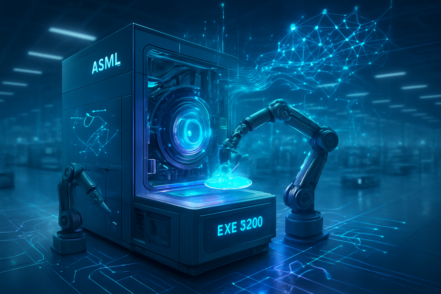
As of January 30, 2026, the global semiconductor landscape is undergoing a tectonic shift. Samsung Electronics (KRX: 005930) has officially reached a critical performance and yield milestone for its 2nm (SF2P) production process, signaling a major challenge to the long-standing dominance of Taiwan Semiconductor Manufacturing Company (NYSE: TSM). Following its Q4 2025 earnings report, Samsung confirmed that its performance-optimized 2nm node, known as SF2P, has successfully hit the 70% yield threshold required for stable mass production—a feat that many industry skeptics thought would take years to master.
This development is more than just a technical victory; it is a strategic lifeline for the world’s largest chip designers. With TSMC’s 2nm capacity currently overwhelmed by exclusive orders from high-priority clients, the emergence of a viable, high-yield alternative from Samsung provides a release valve for a supply chain that has been dangerously bottlenecked. By mastering the intricate Gate-All-Around (GAA) architecture ahead of its rivals, Samsung is positioning itself as the primary destination for the next generation of high-performance AI and mobile processors.
Engineering the Future: The Maturity of 3rd-Gen GAA
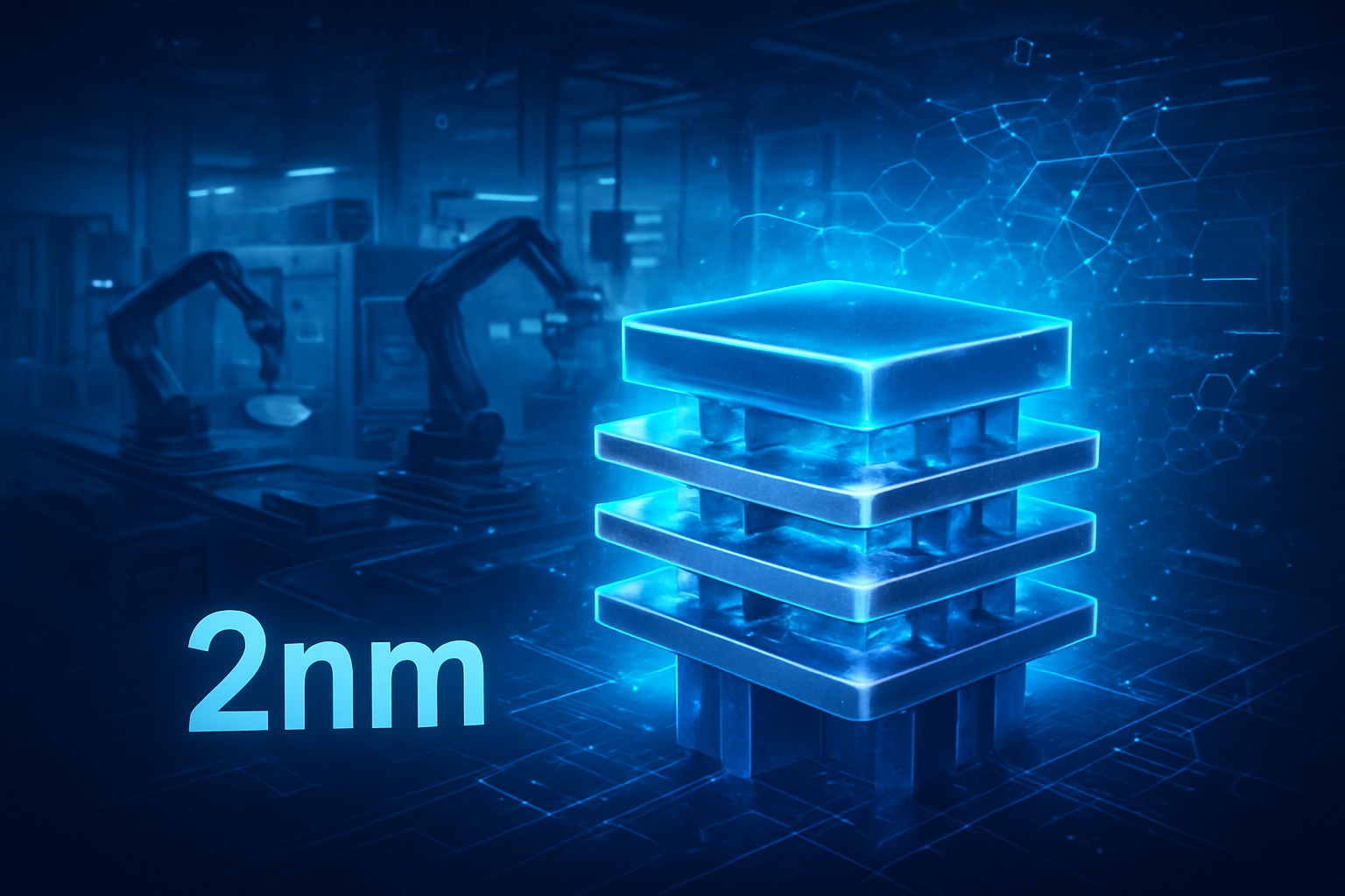
The SF2P node represents the second generation of Samsung’s 2nm platform, specifically optimized for high-performance computing (HPC) and premium mobile devices. Unlike traditional FinFET transistors, which hit physical scaling limits years ago, Samsung’s 2nm utilizes its proprietary Multi-Bridge Channel FET (MBCFET) architecture—a 3rd-generation evolution of GAA technology. This approach allows for a "nanosheet" design where the width of the channel can be adjusted to optimize for either extreme power efficiency or maximum performance. Compared to the first-generation SF2 node, the 2026-era SF2P delivers a 12% boost in clock speeds, a 25% improvement in power efficiency, and an 8% reduction in total die area.
Technical experts note that Samsung’s early gamble on GAA—which it first introduced at the 3nm node while TSMC stuck with FinFET—is finally paying dividends. While competitors are only now navigating the "learning curve" of nanosheet production, Samsung has accumulated four years of telemetry data on GAA manufacturing. This experience has allowed the foundry to refine its extreme ultraviolet (EUV) lithography processes and address the "stochastic" defects that typically plague sub-3nm nodes. The result is a more uniform transistor structure that significantly reduces leakage current, a critical requirement for the power-hungry AI workloads of 2026.
A Strategic Pivot: Qualcomm and AMD Secure Capacity
The immediate beneficiaries of Samsung’s yield breakthrough are Qualcomm (NASDAQ: QCOM) and AMD (NASDAQ: AMD). As of late January 2026, both companies are reportedly in final negotiations to shift significant portions of their 2nm roadmap to Samsung Foundry. The move is driven by a stark reality: TSMC’s 2nm (N2) capacity is nearly 50% reserved by a single customer, leaving other tech giants fighting for leftovers and paying a "wafer premium" that has risen 50% over previous generations. Qualcomm is expected to utilize SF2P for its next-generation Snapdragon series, while AMD is eyeing the node for its "Venice" EPYC server CPUs to ensure supply stability in the face of skyrocketing enterprise demand.
This shift represents a significant competitive disruption. For years, TSMC’s "foundry-only" model gave it a reputation for neutrality and reliability that Samsung, a conglomerate that also makes its own consumer products, struggled to match. However, the sheer scale of the AI boom has forced a "dual-sourcing" strategy among major chip designers. By offering competitive yields and more favorable pricing than TSMC, Samsung is transforming the foundry market from a monopoly into a true duopoly. Furthermore, Samsung’s massive $16.5 billion contract with Tesla (NASDAQ: TSLA) for its AI6 autonomous driving chips has served as a powerful "seal of approval," encouraging other automotive and data center players to reconsider their reliance on a single supplier.
The "One-Stop" AI Solution and the Taylor, Texas Factor
Samsung’s 2nm success is part of a broader "total solution" strategy that integrates logic, memory, and packaging. In January 2026, Samsung began large-scale shipments of its 12-layer HBM4 (High Bandwidth Memory), a key component for AI accelerators used by NVIDIA (NASDAQ: NVDA) and others. By offering 2nm logic manufacturing alongside HBM4 and advanced X-Cube 3D packaging, Samsung provides a vertically integrated stack that reduces latency and power consumption. This "one-stop shop" capability is something neither TSMC nor Intel (NASDAQ: INTC) can currently match with the same level of internal synchronization, making Samsung an attractive partner for startups building custom "Agentic AI" silicon.
The geopolitical dimension of this ramp-up cannot be ignored. Samsung’s Taylor, Texas facility is now 93% complete and is transitioning to a "2nm-first" factory. With trial runs of ASML EUV lithography tools scheduled for March 2026, the Taylor fab is set to become a cornerstone of the "Made in USA" advanced chip initiative. This domestic capacity is a major selling point for U.S.-based companies like AMD and Google, who are under increasing pressure to diversify their manufacturing away from the geopolitical sensitivities of the Taiwan Strait. Samsung’s ability to hit 70% yield in its Korean facilities provides the blueprint for a rapid and successful ramp in the United States.
Looking Ahead: The Road to 1.4nm and Backside Power
While the industry focuses on the SF2P ramp, Samsung’s R&D teams are already moving toward the next frontier. Near-term developments include the introduction of SF2Z in 2027, which will incorporate Backside Power Delivery Network (BSPDN) technology. This innovation moves the power circuitry to the back of the wafer, freeing up the top side for more transistors and further reducing voltage drops. Beyond 2nm, the roadmap points toward the 1.4nm (SF1.4) node, where Samsung expects to apply lessons from its GAA maturity to achieve even more aggressive density gains.
The challenge remains in maintaining these yields as the volume scales to hundreds of thousands of wafers per month. Experts predict that the next 12 months will be a "volume war" as Samsung attempts to match the total output capacity of TSMC’s sprawling "GigaFabs." Additionally, as AI models move from data centers to "on-device" edge environments, the demand for SF2P-class chips will expand into a wider variety of form factors, including wearable AR glasses and advanced robotics. The primary hurdle will be the continued availability of high-NA EUV tools and the specialized gases required for sub-2nm etching.
A New Era for the Semiconductor Industry
Samsung’s achievement of 70% yield on the SF2P node marks a historic comeback for the South Korean giant. After years of trailing TSMC in the transition from 7nm to 5nm and 4nm, Samsung has utilized the radical architecture shift of Gate-All-Around to leapfrog its competition in terms of manufacturing maturity. This development effectively breaks the "TSMC bottleneck," providing the global AI industry with the diversified supply chain it desperately needs to sustain its current pace of innovation.
In the coming weeks, the industry will be watching for the official "tape-out" announcements from Qualcomm and AMD, which will confirm the first commercial products to use this new technology. The successful integration of SF2P into the global supply chain will not only redefine Samsung’s financial trajectory but will also serve as a catalyst for more affordable and efficient AI hardware worldwide. As we move deeper into 2026, the foundry race has officially been reset, and for the first time in a decade, the lead is up for grabs.
This content is intended for informational purposes only and represents analysis of current AI and semiconductor developments.
TokenRing AI delivers enterprise-grade solutions for multi-agent AI workflow orchestration, AI-powered development tools, and seamless remote collaboration platforms.
For more information, visit https://www.tokenring.ai/.