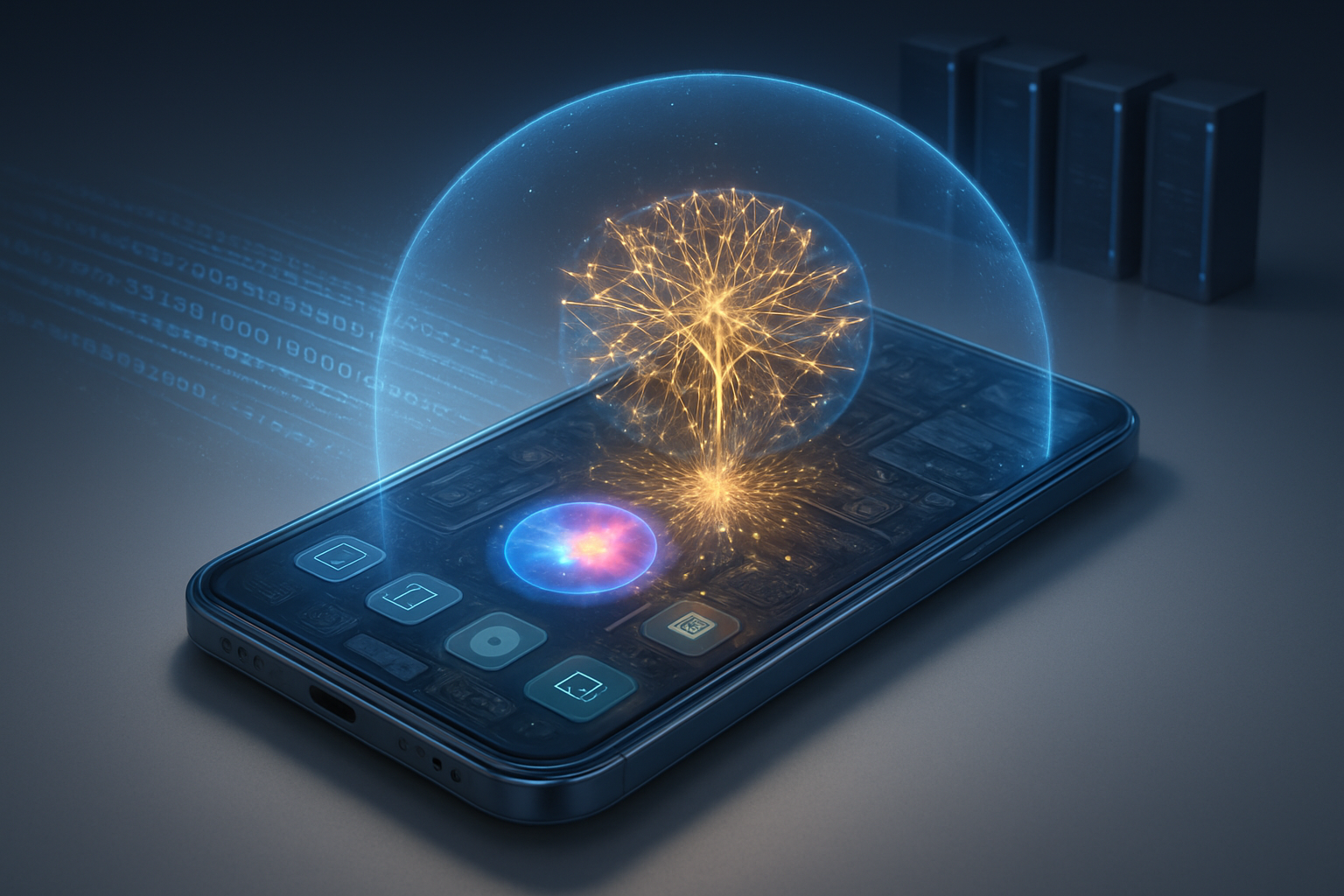
The artificial intelligence industry has reached a pivotal milestone with the widespread adoption of the Model Context Protocol (MCP), an open standard that has effectively solved the "interoperability crisis" that once hindered enterprise AI deployment. Originally introduced by Anthropic in late 2024, the protocol has evolved into the universal language for AI agents, allowing them to move beyond isolated chat interfaces and seamlessly interact with complex data ecosystems including Slack, Google Drive, and GitHub. By January 2026, MCP has become the bedrock of the "Agentic Web," providing a secure, standardized bridge between Large Language Models (LLMs) and the proprietary data silos of the modern corporation.
The significance of this development cannot be overstated; it marks the transition of AI from a curiosity capable of generating text to an active participant in business workflows. Before MCP, developers were forced to build bespoke, non-reusable integrations for every unique combination of AI model and data source—a logistical nightmare known as the "N x M" problem. Today, the protocol has reduced this complexity to a simple plug-and-play architecture, where a single MCP server can serve any compatible AI model, regardless of whether it is hosted by Anthropic, OpenAI, or Google.
Technical Architecture: Bridging the Model-Data Divide
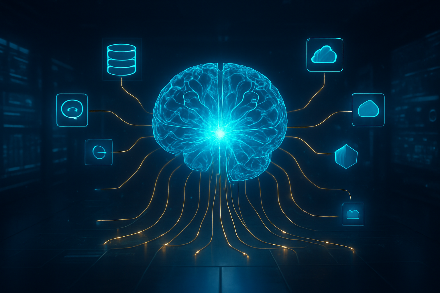
Technically, MCP is a sophisticated framework built on a client-server architecture that utilizes JSON-RPC 2.0-based messaging. At its core, the protocol defines three primary primitives: Resources, which are URI-based data streams like a specific database row or a Slack thread; Tools, which are executable functions like "send an email" or "query SQL"; and Prompts, which act as pre-defined workflow templates that guide the AI through multi-step tasks. This structure allows AI applications to act as "hosts" that connect to various "servers"—lightweight programs that expose specific capabilities of an underlying software or database.
Unlike previous attempts at AI integration, which often relied on rigid API wrappers or fragile "plugin" ecosystems, MCP supports both local communication via standard input/output (STDIO) and remote communication via HTTP with Server-Sent Events (SSE). This flexibility is what has allowed it to scale so rapidly. In late 2025, the protocol was further enhanced with the "MCP Apps" extension (SEP-1865), which introduced the ability for servers to deliver interactive UI components directly into an AI’s chat window. This means an AI can now present a user with a dynamic chart or a fillable form sourced directly from a secure enterprise database, allowing for a collaborative, "human-in-the-loop" experience.
The initial reaction from the AI research community was overwhelmingly positive, as MCP addressed the fundamental limitation of "stale" training data. By providing a secure way for agents to query live data using the user's existing permissions, the protocol eliminated the need to constantly retrain models on new information. Industry experts have likened the protocol’s impact to that of the USB-C standard in hardware or the TCP/IP protocol for the internet—a universal interface that allows diverse systems to communicate without friction.
Strategic Realignment: The Battle for the Enterprise Agent
The shift toward MCP has reshaped the competitive landscape for tech giants. Microsoft (NASDAQ: MSFT) was an early and aggressive adopter, integrating native MCP support into Windows 11 and its Copilot Studio by mid-2025. This allowed Windows itself to function as an MCP server, giving AI agents unprecedented access to local file systems and window management. Similarly, Salesforce (NYSE: CRM) capitalized on the trend by launching official MCP servers for Slack and Agentforce, effectively turning every Slack channel into a structured data source that an AI agent can read from and write to with precision.
Alphabet (NASDAQ: GOOGL) and Amazon (NASDAQ: AMZN) have also realigned their cloud strategies around this standard. Google’s Gemini models now utilize MCP to interface with Google Workspace, while Amazon Web Services has become the primary infrastructure provider for hosting the estimated 10,000+ public and private MCP servers now in existence. This standardization has significantly reduced "vendor lock-in." Enterprises can now swap their underlying LLM provider—moving from a Claude model to a GPT model, for instance—without having to rewrite the complex integration logic that connects their AI to their internal CRM or ERP systems.
Startups have also found a fertile ground within the MCP ecosystem. Companies like Block (NYSE: SQ) and Cloudflare (NYSE: NET) have contributed heavily to the open-source libraries that make building MCP servers easier for small-scale developers. This has led to a democratic expansion of AI capabilities, where even niche software tools can become "AI-ready" overnight by deploying a simple MCP-compliant server.
A Global Standard: The Agentic AI Foundation
The broader significance of MCP lies in its governance. In December 2025, in a move to ensure the protocol remained a neutral industry standard, Anthropic donated MCP to the newly formed Agentic AI Foundation (AAIF) under the umbrella of the Linux Foundation. This move placed the future of AI interoperability in the hands of a consortium that includes Microsoft, OpenAI, and Meta, preventing any single entity from monopolizing the "connective tissue" of the AI economy.
This milestone is frequently compared to the standardization of the web via HTML/HTTP. Just as the web flourished once browsers and servers could communicate through a common language, the "Agentic AI" era has truly begun now that models can interact with data in a predictable, secure manner. However, the rise of MCP has not been without concerns. Security experts have pointed out that while MCP respects existing user permissions, the sheer "autonomy" granted to agents through these connections increases the surface area for potential prompt injection attacks or data leakage if servers are not properly audited.
Despite these challenges, the consensus is that MCP has moved the industry past the "chatbot" phase. We are no longer just talking to models; we are deploying agents that can navigate our digital world. The protocol provides a structured way to audit what an AI did, what data it accessed, and what tools it triggered, providing a level of transparency that was previously impossible with fragmented, ad-hoc integrations.
Future Horizons: From Tools to Teammates
Looking ahead to the remainder of 2026 and beyond, the next frontier for MCP is the development of "multi-agent orchestration." While current implementations typically involve one model connecting to many tools, the AAIF is currently working on standards that allow multiple AI agents—each with their own specialized MCP servers—to collaborate on complex projects. For example, a "Marketing Agent" might use its MCP connection to a creative suite to generate an ad, then pass that asset to a "Legal Agent" with an MCP connection to a compliance database for approval.
Furthermore, we are seeing the emergence of "Personal MCPs," where individuals host their own private servers containing their emails, calendars, and personal files. This would allow a personal AI assistant to operate entirely on the user's local hardware while still possessing the contextual awareness of a cloud-based system. Challenges remain in the realm of latency and the standardization of "reasoning" between different agents, but experts predict that within two years, the majority of enterprise software will be shipped with a built-in MCP server as a standard feature.
Conclusion: The Foundation of the AI Economy
The Model Context Protocol has successfully transitioned from an ambitious proposal by Anthropic to the definitive standard for AI interoperability. By providing a universal interface for resources, tools, and prompts, it has solved the fragmentation problem that threatened to stall the enterprise AI revolution. The protocol’s adoption by giants like Microsoft, Salesforce, and Google, coupled with its governance by the Linux Foundation, ensures that it will remain a cornerstone of the industry for years to come.
As we move into early 2026, the key takeaway is that the "walled gardens" of data are finally coming down—not through the compromise of security, but through the implementation of a better bridge. The impact of MCP is a testament to the power of open standards in driving technological progress. For businesses and developers, the message is clear: the era of the isolated AI is over, and the era of the integrated, agentic enterprise has officially arrived. Watch for an explosion of "agent-first" applications in the coming months as the full potential of this unified ecosystem begins to be realized.
This content is intended for informational purposes only and represents analysis of current AI developments.
TokenRing AI delivers enterprise-grade solutions for multi-agent AI workflow orchestration, AI-powered development tools, and seamless remote collaboration platforms.
For more information, visit https://www.tokenring.ai/.