Blog

  • The Era of ‘Slow AI’: How OpenAI’s o1 and o3 Are Rewriting the Rules of Machine Intelligence

    The Era of ‘Slow AI’: How OpenAI’s o1 and o3 Are Rewriting the Rules of Machine Intelligence

    As of late January 2026, the artificial intelligence landscape has undergone a seismic shift, moving away from the era of "reactive chatbots" to a new paradigm of "deliberative reasoners." This transformation was sparked by the arrival of OpenAI’s o-series models—specifically o1 and the recently matured o3. Unlike their predecessors, which relied primarily on statistical word prediction, these models utilize a "System 2" approach to thinking. By pausing to deliberate and analyze their internal logic before generating a response, OpenAI’s reasoning models have effectively bridged the gap between human-like intuition and PhD-level analytical depth, solving complex scientific and mathematical problems that were once considered the exclusive domain of human experts.

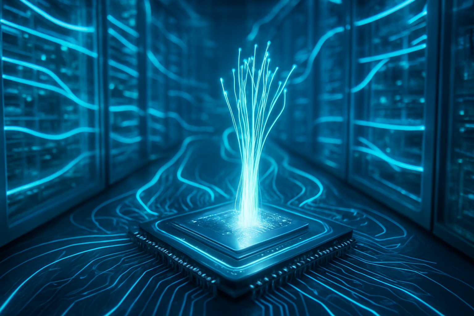
    The immediate significance of the o-series, and the flagship o3-pro model, lies in its ability to scale "test-time compute"—the amount of processing power dedicated to a model while it is thinking. This evolution has moved the industry past the plateau of pre-training scaling laws, demonstrating that an AI can become significantly smarter not just by reading more data, but by taking more time to contemplate the problem at hand.

    The Technical Foundations of Deliberative Cognition

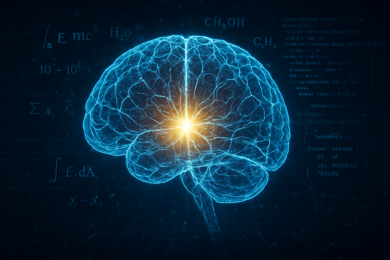
    The technical breakthrough behind OpenAI o1 and o3 is rooted in the psychological framework of "System 1" and "System 2" thinking, popularized by Daniel Kahneman. While previous models like GPT-4o functioned as System 1—intuitive, fast, and prone to "hallucinations" because they predict the very next token without a look-ahead—the o-series engages System 2. This is achieved through a hidden, internal Chain of Thought (CoT). When a user prompts the model with a difficult query, the model generates thousands of internal "thinking tokens" that are never shown to the user. During this process, the model brainstorms multiple solutions, cross-references its own logic, and identifies errors before ever producing a final answer.

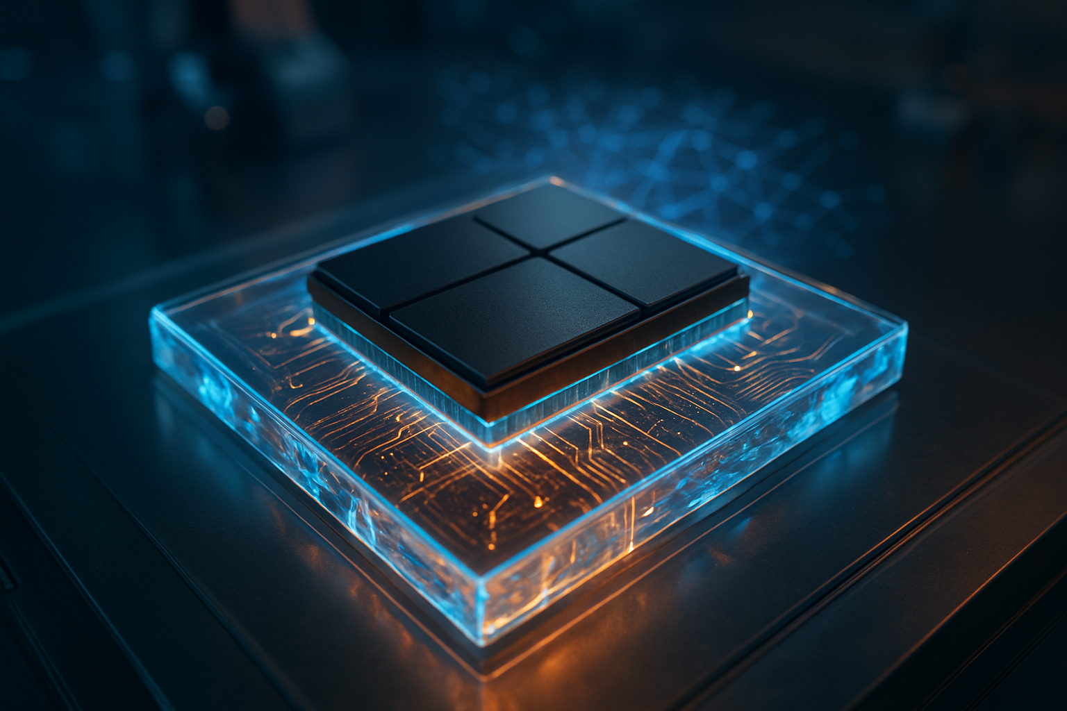
    Underpinning this capability is a massive application of Reinforcement Learning (RL). Unlike standard Large Language Models (LLMs) that are trained to mimic human writing, the o-series was trained using outcome-based and process-based rewards. The model is incentivized to find the correct answer and rewarded for the logical steps taken to get there. This allows o3 to perform search-based optimization, exploring a "tree" of possible reasoning paths (similar to how AlphaGo considers moves in a board game) to find the most mathematically sound conclusion. The results are staggering: on the GPQA Diamond, a benchmark of PhD-level science questions, o3-pro has achieved an accuracy rate of 87.7%, surpassing the performance of human PhDs. In mathematics, o3 has achieved near-perfect scores on the AIME (American Invitational Mathematics Examination), placing it in the top tier of competitive mathematicians globally.

    The Competitive Shockwave and Market Realignment

    The release and subsequent dominance of the o3 model have forced a radical pivot among big tech players and AI startups. Microsoft (NASDAQ:MSFT), OpenAI’s primary partner, has integrated these reasoning capabilities into its "Copilot" ecosystem, effectively turning it from a writing assistant into an autonomous research agent. Meanwhile, Alphabet (NASDAQ:GOOGL), via Google DeepMind, responded with Gemini 2.0 and the "Deep Think" mode, which distills the mathematical rigor of its AlphaProof and AlphaGeometry systems into a commercial LLM. Google’s edge remains in its multimodal speed, but OpenAI’s o3-pro continues to hold the "reasoning crown" for ultra-complex engineering tasks.

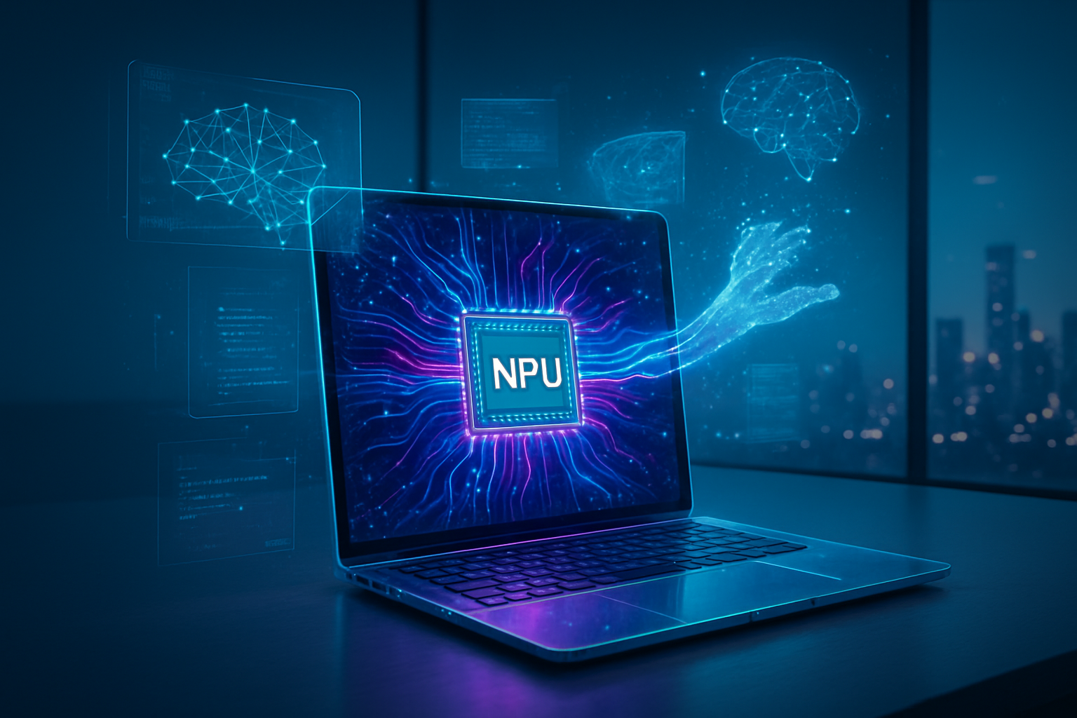
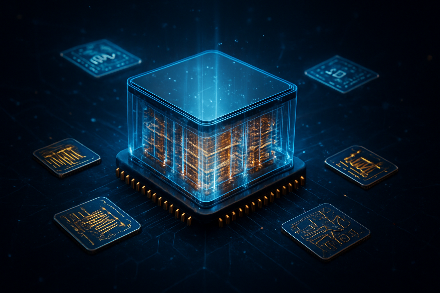
    The hardware sector has also been reshaped by this shift toward test-time compute. NVIDIA (NASDAQ:NVDA) has capitalized on the demand for inference-heavy workloads with its newly launched Rubin (R100) platform, which is optimized for the sequential "thinking" tokens required by reasoning models. Startups are also feeling the heat; the "wrapper" companies that once built simple chat interfaces are being disrupted by "agentic" startups like Cognition AI and others who use the reasoning power of o3 to build autonomous software engineers and scientific researchers. The strategic advantage has shifted from those who have the most data to those who can most efficiently orchestrate "thinking time."

    AGI Milestones and the Ethics of Deliberation

    The wider significance of the o3 model is most visible in its performance on the ARC-AGI benchmark, a test designed to measure "fluid intelligence" or the ability to solve novel problems that the model hasn't seen in its training data. In 2025, o3 achieved a historic score of 87.5%, a feat many researchers believed was years, if not decades, away. This milestone suggests that we are no longer just building sophisticated databases, but are approaching a form of Artificial General Intelligence (AGI) that can reason through logic-based puzzles with human-like adaptability.

    However, this "System 2" shift introduces new concerns. The internal reasoning process of these models is largely a "black box," hidden from the user to prevent the model’s chain-of-thought from being reverse-engineered or used to bypass safety filters. While OpenAI employs "deliberative alignment"—where the model reasons through its own safety policies before answering—critics argue that this internal monologue makes the models harder to audit for bias or deceptive behavior. Furthermore, the immense energy cost of "test-time compute" has sparked renewed debate over the environmental sustainability of scaling AI intelligence through brute-force deliberation.

    The Road Ahead: From Reasoning to Autonomous Agents

    Looking toward the remainder of 2026, the industry is moving toward "Unified Models." We are already seeing the emergence of systems like GPT-5, which act as a reasoning router. Instead of a user choosing between a "fast" model and a "thinking" model, the unified AI will automatically determine how much "effort" a task requires—instantly replying to a greeting, but pausing for 30 seconds to solve a calculus problem. This intelligence will increasingly be deployed in autonomous agents capable of long-horizon planning, such as conducting multi-day market research or managing complex supply chains without human intervention.

    The next frontier for these reasoning models is embodiment. As companies like Tesla (NASDAQ:TSLA) and various robotics labs integrate o-series-level reasoning into humanoid robots, we expect to see machines that can not only follow instructions but reason through physical obstacles and complex mechanical repairs in real-time. The challenge remains in reducing the latency and cost of this "thinking time" to make it viable for edge computing and mobile devices.

    A Historic Pivot in AI History

    OpenAI’s o1 and o3 models represent a turning point that will likely be remembered as the end of the "Chatbot Era" and the beginning of the "Reasoning Era." By moving beyond simple pattern matching and next-token prediction, OpenAI has demonstrated that intelligence can be synthesized through deliberate logic and reinforcement learning. The shift from System 1 to System 2 thinking has unlocked the potential for AI to serve as a genuine collaborator in scientific discovery, advanced engineering, and complex decision-making.

    As we move deeper into 2026, the industry will be watching closely to see how competitors like Anthropic (backed by Amazon (NASDAQ:AMZN)) and Google attempt to bridge the reasoning gap. For now, the "Slow AI" movement has proven that sometimes, the best way to move forward is to take a moment and think.


    This content is intended for informational purposes only and represents analysis of current AI developments.

    TokenRing AI delivers enterprise-grade solutions for multi-agent AI workflow orchestration, AI-powered development tools, and seamless remote collaboration platforms.
    For more information, visit https://www.tokenring.ai/.

  • The $5 Million Miracle: How the ‘DeepSeek-R1 Shock’ Ended the Era of Brute-Force AI Scaling

    The $5 Million Miracle: How the ‘DeepSeek-R1 Shock’ Ended the Era of Brute-Force AI Scaling

    Exactly one year after the release of DeepSeek-R1, the global technology landscape continues to reel from what is now known as the "DeepSeek Shock." In late January 2025, a relatively obscure Chinese laboratory, DeepSeek, released a reasoning model that matched the performance of OpenAI’s state-of-the-art o1 model—but with a staggering twist: it was trained for a mere $5.6 million. This announcement didn't just challenge the dominance of Silicon Valley; it shattered the "compute moat" that had driven hundreds of billions of dollars in infrastructure investment, leading to the largest single-day market cap loss in history for NVIDIA (NASDAQ: NVDA).

    The immediate significance of DeepSeek-R1 lay in its defiance of "Scaling Laws"—the industry-wide belief that superior intelligence could only be achieved through exponential increases in data and compute power. By achieving frontier-level logic, mathematics, and coding capabilities on a budget that represents less than 0.1% of the projected training costs for models like GPT-5, DeepSeek proved that algorithmic efficiency could outpace brute-force hardware. As of January 28, 2026, the industry has fundamentally pivoted, moving away from "cluster-maximalism" and toward the "DeepSeek-style" lean architecture that prioritized architectural ingenuity over massive GPU arrays.

    Breaking the Compute Moat: The Technical Triumph of R1

    DeepSeek-R1 achieved its parity with OpenAI o1 by utilizing a series of architectural innovations that bypassed the traditional bottlenecks of Large Language Models (LLMs). Most notable was the implementation of Multi-head Latent Attention (MLA) and a refined Mixture-of-Experts (MoE) framework. Unlike dense models that activate all parameters for every task, DeepSeek-R1’s MoE architecture only engaged a fraction of its neurons per query, dramatically reducing the energy and compute required for both training and inference. The model was trained on a relatively modest cluster of approximately 2,000 NVIDIA H800 GPUs—a far cry from the 100,000-unit clusters rumored to be in use by major U.S. labs.

    Technically, DeepSeek-R1 focused on "Reasoning-via-Reinforcement Learning," a process where the model was trained to "think out loud" through a chain-of-thought process without requiring massive amounts of human-annotated data. In benchmarks that defined the 2025 AI era, DeepSeek-R1 scored a 79.8% on the AIME 2024 math benchmark, slightly edging out OpenAI o1’s 79.2%. In coding, it achieved a 96.3rd percentile on Codeforces, proving that it wasn't just a budget alternative, but a world-class reasoning engine. The AI research community was initially skeptical, but once the weights were open-sourced and verified, the consensus shifted: the "efficiency wall" had been breached.

    Market Carnage and the Strategic Pivot of Big Tech

    The market reaction to the DeepSeek-R1 revelation was swift and brutal. On January 27, 2025, just days after the model’s full capabilities were understood, NVIDIA (NASDAQ: NVDA) saw its stock price plummet by nearly 18%, erasing roughly $600 billion in market capitalization in a single trading session. This "NVIDIA Shock" was triggered by a sudden realization among investors: if frontier AI could be built for $5 million, the projected multi-billion-dollar demand for NVIDIA’s H100 and Blackwell chips might be an over-leveraged bubble. The "arms race" for hardware suddenly looked like a race to own expensive, soon-to-be-obsolete hardware.

    This disruption sent shockwaves through the "Magnificent Seven." Companies like Microsoft (NASDAQ: MSFT) and Alphabet (NASDAQ: GOOGL), which had committed tens of billions to massive data centers, were forced to defend their capital expenditures to jittery shareholders. Conversely, Meta (NASDAQ: META) and independent developers benefited immensely from the DeepSeek-R1 release, as the model's open-source nature allowed startups to integrate reasoning capabilities into their own products without paying the "OpenAI tax." The strategic advantage shifted from those who owned the most chips to those who could design the most efficient algorithms.

    Redefining the Global AI Landscape

    The "DeepSeek Shock" is now viewed as the most significant AI milestone since the release of ChatGPT. It fundamentally altered the geopolitical landscape of AI, proving that Chinese firms could achieve parity with U.S. labs despite heavy export restrictions on high-end semiconductors. By utilizing the aging H800 chips—specifically designed to comply with U.S. export controls—DeepSeek demonstrated that ingenuity could circumvent political barriers. This has led to a broader re-evaluation of AI "scaling laws," with many researchers now arguing that we are entering an era of "Diminishing Returns on Compute" and "Exponential Returns on Architecture."

    However, the shock also raised concerns regarding AI safety and alignment. Because DeepSeek-R1 was released with open weights and minimal censorship, it sparked a global debate on the democratization of powerful reasoning models. Critics argued that the ease of training such models could allow bad actors to create sophisticated cyber-threats or biological weapons for a fraction of the cost previously imagined. Comparisons were drawn to the "Sputnik Moment," as the U.S. government scrambled to reassess its lead in the AI sector, realizing that the "compute moat" was a thinner defense than previously thought.

    The Horizon: DeepSeek V4 and the Rise of mHC

    As we look forward from January 2026, the momentum from the R1 shock shows no signs of slowing. Current leaks regarding the upcoming DeepSeek V4 (internally known as Project "MODEL1") suggest that the lab is now targeting the dominance of Claude 3.5 and the unreleased GPT-5. Reports indicate that V4 utilizes a new "Manifold-Constrained Hyper-Connections" (mHC) architecture, which supposedly allows for even deeper model layers without the traditional training instabilities that plague current LLMs. This could theoretically allow for models with trillions of parameters that still run on consumer-grade hardware.

    Experts predict that the next 12 months will see a "race to the bottom" in terms of inference costs, making AI intelligence a cheap, ubiquitous commodity. The focus is shifting toward "Agentic Workflows"—where models like DeepSeek-R1 don't just answer questions but autonomously execute complex software engineering and research tasks. The primary challenge remaining is "Reliability at Scale"; while DeepSeek-R1 is a logic powerhouse, it still occasionally struggles with nuanced linguistic instruction-following compared to its more expensive American counterparts—a gap that V4 is expected to close.

    A New Era of Algorithmic Supremacy

    The DeepSeek-R1 shock will be remembered as the moment the AI industry grew up. It ended the "Gold Rush" phase of indiscriminate hardware spending and ushered in a "Renaissance of Efficiency." The key takeaway from the past year is that intelligence is not a function of how much electricity you can burn, but how elegantly you can structure information. DeepSeek's $5.6 million miracle proved that the barrier to entry for "God-like AI" is much lower than Silicon Valley wanted to believe.

    In the coming weeks and months, the industry will be watching for the official launch of DeepSeek V4 and the response from OpenAI and Anthropic. If the trend of "more for less" continues, we may see a massive consolidation in the chip industry and a total reimagining of the AI business model. The "DeepSeek Shock" wasn't just a market event; it was a paradigm shift that ensured the future of AI would be defined by brains, not just brawn.


    This content is intended for informational purposes only and represents analysis of current AI developments.

    TokenRing AI delivers enterprise-grade solutions for multi-agent AI workflow orchestration, AI-powered development tools, and seamless remote collaboration platforms. For more information, visit https://www.tokenring.ai/.

  • The Brain in the Box: Intel’s Billion-Neuron Breakthroughs Signal the End of the Power-Hungry AI Era

    The Brain in the Box: Intel’s Billion-Neuron Breakthroughs Signal the End of the Power-Hungry AI Era

    In a landmark shift for the semiconductor industry, the dawn of 2026 has brought the "neuromorphic revolution" from the laboratory to the front lines of enterprise computing. Intel (NASDAQ: INTC) has officially transitioned its Loihi architecture into a new era of scale, moving beyond experimental prototypes to massive, billion-neuron systems that mimic the human brain’s biological efficiency. These systems, led by the flagship Hala Point cluster, are now demonstrating the ability to process complex AI sensory data and optimization workloads using 100 times less power than traditional high-end CPUs, marking a critical turning point in the global effort to make artificial intelligence sustainable.

    This development arrives at a pivotal moment. As traditional data centers struggle under the massive energy demands of Large Language Models (LLMs) and generative AI, Intel’s neuromorphic advancements offer a radically different path. By processing information using "spikes"—discrete pulses of electricity that occur only when data changes—these chips eliminate the constant power draw inherent in conventional Von Neumann architectures. This efficiency isn't just a marginal gain; it is a fundamental reconfiguration of how machines think, allowing for real-time, continuous learning in devices ranging from autonomous drones to industrial robotics without the need for massive cooling systems or grid-straining power supplies.

    The technical backbone of this breakthrough lies in the evolution of the Loihi 2 processor and its successor, the newly unveiled Loihi 3. While traditional chips are built around synchronized clocks and constant data movement between memory and the CPU, the Loihi 2 architecture integrates memory directly with processing logic at the "neuron" level. Each chip supports up to 1 million neurons and 120 million synapses, but the true innovation is in its "graded spikes." Unlike earlier neuromorphic designs that used simple binary on/off signals, these graded spikes allow for multi-dimensional data to be transmitted in a single pulse, vastly increasing the information density of the network while maintaining a microscopic power footprint.

    The scaling of these chips into the Hala Point system represents the pinnacle of current neuromorphic engineering. Hala Point integrates 1,152 Loihi 2 processors into a chassis no larger than a microwave oven, supporting a staggering 1.15 billion neurons and 128 billion synapses. This system achieves a performance metric of 20 quadrillion operations per second (petaops) with a peak power draw of only 2,600 watts. For comparison, achieving similar throughput on a traditional GPU-based cluster would require nearly 100 times that energy, often necessitating specialized liquid cooling.

    Industry experts have been quick to note the departure from "brute-force" AI. Dr. Mike Davies, director of Intel’s Neuromorphic Computing Lab, highlighted that while traditional AI models are essentially static after training, the Hala Point system supports "on-device learning," allowing the system to adapt to new environments in real-time. This capability has been validated by initial research from Sandia National Laboratories, where the hardware was used to solve complex optimization problems—such as real-time logistics and satellite pathfinding—at speeds that left modern server-grade processors in the dust.

    The implications for the technology sector are profound, particularly for companies focused on "Edge AI" and robotics. Intel’s advancement places it in a unique competitive position against NVIDIA (NASDAQ: NVDA), which currently dominates the AI landscape through its high-powered H100 and B200 GPUs. While NVIDIA focuses on massive training clusters for LLMs, Intel is carving out a near-monopoly on high-efficiency inference and physical AI. This shift is likely to benefit firms specializing in autonomous systems, such as Tesla (NASDAQ: TSLA) and Boston Dynamics, who require immense on-board processing power without the weight and heat of traditional hardware.

    Furthermore, the emergence of IBM (NYSE: IBM) as a key player in the neuromorphic space with its NorthPole architecture and 3D Analog In-Memory Computing (AIMC) creates a two-horse race for the future of "Green AI." IBM's 2026 production-ready NorthPole chips are specifically targeting computer vision and Mixture-of-Experts (MoE) models, claiming energy efficiency gains of up to 1,000x for specific tasks. This competition is forcing a strategic pivot across the industry: major AI labs, once obsessed solely with model size, are now prioritizing "efficiency-first" architectures to lower the Total Cost of Ownership (TCO) for their enterprise clients.

    Startups like BrainChip (ASX: BRN) are also finding a foothold in this new ecosystem. By focusing on ultra-low-power "Akida" processors for IoT and automotive monitoring, these smaller players are proving that neuromorphic technology can be commercialized today, not just in a decade. As these efficient chips become more widely available, we can expect a disruption in the cloud service provider market; companies like Amazon (NASDAQ: AMZN) and Microsoft (NASDAQ: MSFT) may soon offer "Neuromorphic-as-a-Service" for clients whose workloads are too sensitive to latency or power costs for traditional cloud setups.

    The wider significance of the billion-neuron breakthrough cannot be overstated. For the past decade, the AI industry has been criticized for its "compute-at-any-cost" mentality, where the environmental impact of training a single model can equal the lifetime emissions of several automobiles. Neuromorphic computing directly addresses the "energy wall" that many predicted would stall AI progress. By proving that a system can simulate over a billion neurons with the power draw of a household appliance, Intel has demonstrated that AI growth does not have to be synonymous with environmental degradation.

    This milestone mirrors previous historic shifts in computing, such as the transition from vacuum tubes to transistors. In the same way that transistors allowed computers to move from entire rooms to desktops, neuromorphic chips are allowing high-level intelligence to move from massive data centers to the "edge" of the network. There are, however, significant hurdles. The software stack for neuromorphic chips—primarily Spiking Neural Networks (SNNs)—is fundamentally different from the backpropagation algorithms used in today’s deep learning. This creates a "programming gap" that requires a new generation of developers trained in event-based computing rather than traditional frame-based processing.

    Societal concerns also loom, particularly regarding privacy and security. If highly capable AI can run locally on a drone or a pair of glasses with 100x efficiency, the need for data to be sent to a central, regulated cloud diminishes. This could lead to a proliferation of untraceable, "always-on" AI surveillance tools that operate entirely off the grid. As the barrier to entry for high-performance AI drops, regulatory bodies will likely face new challenges in governing distributed, autonomous intelligence that doesn't rely on massive, easily-monitored data centers.

    Looking ahead, the next two years are expected to see the convergence of neuromorphic hardware with "Foundation Models." Researchers are already working on "Analog Foundation Models" that can run on Loihi 3 or IBM’s NorthPole with minimal accuracy loss. By 2027, experts predict we will see the first "Human-Scale" neuromorphic computer. Projects like DeepSouth at Western Sydney University are already aiming for 100 billion neurons—the approximate count of a human brain—using neuromorphic architectures to achieve real-time simulation speeds that were previously thought to be decades away.

    In the near term, the most immediate applications will be in scientific supercomputing and robotics. The development of the "NeuroFEM" algorithm allows these chips to solve partial differential equations (PDEs), which are used in everything from weather forecasting to structural engineering. This transforms neuromorphic chips from "AI accelerators" into general-purpose scientific tools. We can also expect to see "Hybrid AI" systems, where a traditional GPU handles the heavy lifting of training a model, while a neuromorphic chip like Loihi 3 handles the high-efficiency, real-time deployment and adaptation of that model in the physical world.

    Challenges remain, particularly in the standardization of hardware. Currently, an SNN designed for Intel hardware cannot easily run on IBM’s architecture. Industry analysts predict that the next 18 months will see a push for a "Universal Neuromorphic Language," similar to how CUDA standardized GPU programming. If the industry can agree on a common framework, the adoption of these billion-neuron systems could accelerate even faster than the current GPU-based AI boom.

    In summary, the advancements in Intel’s Loihi 2 and Loihi 3 architectures, and the operational success of the Hala Point system, represent a paradigm shift in artificial intelligence. By mimicking the architecture of the brain, Intel has solved the energy crisis that threatened to cap the potential of AI. The move to billion-neuron systems provides the scale necessary for truly intelligent, autonomous machines that can interact with the world in real-time, learning and adapting without the tether of a power cord or a data center connection.

    The significance of this development in AI history is likely to be viewed as the moment AI became "embodied." No longer confined to the digital vacuum of the cloud, intelligence is now moving into the physical fabric of our world. As we look toward the coming weeks, the industry will be watching for the first third-party benchmarks of the Loihi 3 chip and the announcement of more "Brain-Scale" systems. The era of brute-force AI is ending; the era of efficient, biological-scale intelligence has begun.


    This content is intended for informational purposes only and represents analysis of current AI developments.

    TokenRing AI delivers enterprise-grade solutions for multi-agent AI workflow orchestration, AI-powered development tools, and seamless remote collaboration platforms.
    For more information, visit https://www.tokenring.ai/.

  • The Photonic Pivot: Silicon Photonics and CPO Slash AI Power Demands by 50% as the Copper Era Ends

    The Photonic Pivot: Silicon Photonics and CPO Slash AI Power Demands by 50% as the Copper Era Ends

    The transition from moving data via electricity to moving it via light—Silicon Photonics—has officially moved from the laboratory to the backbone of the world's largest AI clusters. By integrating optical engines directly into the processor package through Co-Packaged Optics (CPO), the industry is achieving a staggering 50% reduction in total networking energy consumption, effectively dismantling the "Power Wall" that threatened to stall AI progress.

    This technological leap comes at a critical juncture where the scale of AI training clusters has surged to over one million GPUs. At these "Gigascale" densities, traditional copper-based interconnects have hit a physical limit known as the "Copper Wall," where the energy required to push electrons through metal generates more heat than usable signal. The emergence of CPO in 2026 represents a fundamental reimagining of how computers talk to each other, replacing power-hungry copper cables and discrete optical modules with light-based interconnects that reside on the same silicon substrate as the AI chips themselves.

    The End of the Digital Signal Processor (DSP) Dominance

    The technical catalyst for this revolution is the successful commercialization of 1.6-Terabit (1.6T) per second networking speeds. Previously, data centers relied on "pluggable" optical modules—small boxes that converted electrical signals to light at the edge of a switch. However, at 2026 speeds of 224 Gbps per lane, these pluggables required massive amounts of power for Digital Signal Processors (DSPs) to maintain signal integrity. By contrast, Co-Packaged Optics (CPO) eliminates the long electrical traces between the switch chip and the optical module, allowing for "DSP-lite" or even "DSP-less" architectures.

    The technical specifications of this shift are profound. In early 2024, the energy intensity of moving a bit of data across a network was approximately 15 picojoules per bit (pJ/bit). Today, in January 2026, CPO-integrated systems from industry leaders have slashed that figure to just 5–6 pJ/bit. This 70% reduction in the optical layer translates to an overall networking power saving of up to 50% when factoring in reduced cooling requirements and simplified circuit designs. Furthermore, the adoption of TSMC (NYSE: TSM) Compact Universal Photonic Engine (COUPE) technology has allowed manufacturers to 3D-stack optical components directly onto electrical silicon, increasing bandwidth density to over 1 Tbps per millimeter—a feat previously thought impossible.

    The New Hierarchy: Semiconductors Giants vs. Traditional Networking

    The shift to light has fundamentally reshaped the competitive landscape, shifting power away from traditional networking equipment providers toward semiconductor giants with advanced packaging capabilities. NVIDIA (NASDAQ: NVDA) has solidified its dominance in early 2026 with the mass shipment of its Quantum-X800 and Spectrum-X800 platforms. These are the world's first 3D-stacked CPO switches, designed to save individual data centers tens of megawatts of power—enough to power a small city.

    Broadcom (NASDAQ: AVGO) has similarly asserted its leadership with the launch of the Tomahawk 6, codenamed "Davisson." This 102.4 Tbps switch is the first to achieve volume production for 200G/lane connectivity, a milestone that Meta (NASDAQ: META) validated earlier this quarter by documenting over one million link hours of flap-free operation. Meanwhile, Marvell (NASDAQ: MRVL) has integrated "Photonic Fabric" technology into its custom accelerators following its strategic acquisitions in late 2025, positioning itself as a key rival in the specialized "AI Factory" market. Intel (NASDAQ: INTC) has also pivoted, moving away from pluggable modules to focus on its Optical Compute Interconnect (OCI) chiplets, which are now being sampled for the upcoming "Jaguar Shores" architecture expected in 2027.

    Solving the Power Wall and the Sustainability Crisis

    The broader significance of Silicon Photonics cannot be overstated; it is the "only viable path" to sustainable AI growth, according to recent reports from IDC and Tirias Research. As global AI infrastructure spending is projected to exceed $2 trillion in 2026, the industry is moving away from an "AI at any cost" mentality. Performance-per-watt has replaced raw FLOPS as the primary metric for procurement. The "Power Wall" was not just a technical hurdle but a financial and environmental one, as the energy costs of cooling massive copper-based clusters began to rival the cost of the hardware itself.

    This transition is also forcing a transformation in data center design. Because CPO-integrated switches like NVIDIA’s X800-series generate such high thermal density in a small area, liquid cooling has officially become the industry standard for 2026 deployments. This shift has marginalized traditional air-cooling vendors while creating a massive boom for thermal management specialists. Furthermore, the ability of light to travel hundreds of meters without signal degradation allows for "disaggregated" data centers, where GPUs can be spread across multiple racks or even rooms while still functioning as a single, cohesive processor.

    The Horizon: From CPO to Optical Computing

    Looking ahead, the roadmap for Silicon Photonics suggests that CPO is only the beginning. Near-term developments are expected to focus on bringing optical interconnects even closer to the compute core—moving from the "side" of the chip to the "top" of the chip. Experts at the 2026 HiPEAC conference predicted that by 2028, we will see the first commercial "optical chip-to-chip" communication, where the traces between a GPU and its High Bandwidth Memory (HBM) are replaced by light, potentially reducing energy consumption by another order of magnitude.

    However, challenges remain. The industry is still grappling with the complexities of testing and repairing co-packaged components; unlike a pluggable module, if an optical engine fails in a CPO system, the entire switch or processor may need to be replaced. This has spurred a new market for "External Laser Sources" (ELS), which allow the most failure-prone part of the system—the laser—to remain a hot-swappable component while the photonics stay integrated.

    A Milestone in the History of Computing

    The widespread adoption of Silicon Photonics and CPO in 2026 will likely be remembered as the moment the physical limits of electricity were finally bypassed. By cutting networking energy consumption by 50%, the industry has bought itself at least another decade of the scaling laws that have defined the AI revolution. The move to light is not just an incremental upgrade; it is a foundational change in how humanity builds its most powerful tools.

    In the coming weeks, watch for further announcements from the Open Compute Project (OCP) regarding standardized testing protocols for CPO, as well as the first revenue reports from the 1.6T deployment cycle. As the "Copper Era" fades, the "Photonic Era" is proving that the future of artificial intelligence is not just faster, but brighter and significantly more efficient.


    This content is intended for informational purposes only and represents analysis of current AI developments.

    TokenRing AI delivers enterprise-grade solutions for multi-agent AI workflow orchestration, AI-powered development tools, and seamless remote collaboration platforms.
    For more information, visit https://www.tokenring.ai/.

  • The Silicon Sovereignty: How the AI PC Revolution Redefined Computing in 2026

    The Silicon Sovereignty: How the AI PC Revolution Redefined Computing in 2026

    As of January 2026, the long-promised "AI PC" has transitioned from a marketing catchphrase into the dominant paradigm of personal computing. Driven by the massive hardware refresh cycle following the retirement of Windows 10 in late 2025, over 55% of all new laptops and desktops hitting the market today feature dedicated Neural Processing Units (NPUs) capable of at least 40 Trillion Operations Per Second (TOPS). This shift represents the most significant architectural change to the personal computer since the introduction of the Graphical User Interface (GUI), moving the "brain" of the computer away from general-purpose processing and toward specialized, local artificial intelligence.

    The immediate significance of this revolution is the death of "cloud latency" for daily tasks. In early 2026, users no longer wait for a remote server to process their voice commands, summarize their meetings, or generate high-resolution imagery. By performing inference locally on specialized silicon, devices from Intel (NASDAQ: INTC), AMD (NASDAQ: AMD), and Qualcomm (NASDAQ: QCOM) have unlocked a level of privacy, speed, and battery efficiency that was technically impossible just 24 months ago.

    The NPU Arms Race: Technical Sovereignty on the Desktop

    The technical foundation of the 2026 AI PC rests on three titan architectures that matured throughout 2024 and 2025: Intel’s Lunar Lake (and the newly released Panther Lake), AMD’s Ryzen AI 300 "Strix Point," and Qualcomm’s Snapdragon X Elite series. While previous generations of processors relied on the CPU for logic and the GPU for graphics, these modern chips dedicate significant die area to the NPU. This specialized hardware is designed specifically for the matrix multiplication required by Large Language Models (LLMs) and Diffusion models, allowing them to run at a fraction of the power consumption required by a traditional GPU.

    Intel’s Lunar Lake, which served as the mainstream baseline throughout 2025, pioneered the 48-TOPS NPU that set the standard for Microsoft’s (NASDAQ: MSFT) Copilot+ PC designation. However, as of January 2026, the focus has shifted to Intel’s Panther Lake, built on the cutting-edge Intel 18A process, which pushes NPU performance to 50 TOPS and total platform throughput to 180 TOPS. Meanwhile, AMD’s Strix Point and its 2026 successor, "Gorgon Point," have carved out a niche for "unplugged performance." These chips utilize a multi-die approach that allows for superior multi-threaded performance, making them the preferred choice for developers running local model fine-tuning or heavy "Agentic" workflows.

    Qualcomm has arguably seen the most dramatic rise, with its Snapdragon X2 Elite currently leading the market in raw NPU throughput at a staggering 80 TOPS. This leap is critical for the "Agentic AI" era, where an AI is not just a chatbot but a persistent background process that can see the screen, manage a user’s inbox, and execute complex cross-app tasks autonomously. Unlike the 2024 era of AI, which struggled with high power draw, the 2026 Snapdragon chips enable these background "agents" to run for over 25 hours on a single charge, a feat that has finally validated the "Windows on ARM" ecosystem.

    Market Disruptions: Silicon Titans and the End of Cloud Dependency

    The shift toward local AI inference has fundamentally altered the strategic positioning of the world's largest tech companies. Intel, AMD, and Qualcomm are no longer just selling "faster" chips; they are selling "smarter" chips that reduce a corporation's reliance on expensive cloud API credits. This has created a competitive friction with cloud giants who previously controlled the AI narrative. As local models like Meta’s Llama 4 and Google’s (NASDAQ: GOOGL) Gemma 3 become the standard for on-device processing, the business model of charging per-token for basic AI tasks is rapidly eroding.

    Major software vendors have been forced to adapt. Adobe (NASDAQ: ADBE), for instance, has integrated its Firefly generative engine directly into the NPU-accelerated path of Creative Cloud. In 2026, "Generative Fill" in Photoshop can be performed entirely offline on an 80-TOPS machine, eliminating the need for cloud credits and ensuring that sensitive creative assets never leave the user's device. This "local-first" approach has become a primary selling point for enterprise customers who are increasingly wary of the data privacy implications and spiraling costs of centralized AI.

    Furthermore, the rise of the AI PC has forced Apple (NASDAQ: AAPL) to accelerate its own M-series silicon roadmap. While Apple was an early pioneer of the "Neural Engine," the aggressive 2026 targets set by Qualcomm and Intel have challenged Apple’s perceived lead in efficiency. The market is now witnessing a fierce battle for the "Pro" consumer, where the definition of a high-end machine is no longer measured by core count, but by how many billions of parameters a laptop can process per second without spinning up a fan.

    Privacy, Agency, and the Broader AI Landscape

    The broader significance of the 2026 AI PC revolution lies in the democratization of privacy. In the "Cloud AI" era (2022–2024), users had to trade their data for intelligence. In 2026, the AI PC has decoupled the two. Personal assistants can now index a user’s entire life—emails, photos, browsing history, and documents—to provide hyper-personalized assistance without that data ever touching a third-party server. This has effectively mitigated the "privacy paradox" that once threatened to slow AI adoption in sensitive sectors like healthcare and law.

    This development also marks the transition from "Generative AI" to "Agentic AI." Previous AI milestones focused on the ability to generate text or images; the 2026 milestone is about action. With 80-TOPS NPUs, PCs can now host "Physical AI" models that understand the spatial and temporal context of what a user is doing. If a user mentions a meeting in a video call, the local AI agent can automatically cross-reference their calendar, draft a summary, and file a follow-up task in a project management tool, all through local inference.

    However, this revolution is not without concerns. The "AI Divide" has become a reality, as users on legacy, non-NPU hardware are increasingly locked out of the modern software ecosystem. Developers are now optimizing "NPU-first," leaving those with 2023-era machines with a degraded, slower, and more expensive experience. Additionally, the rise of local AI has sparked new debates over "local misinformation," where highly realistic deepfakes can be generated at scale on consumer hardware without the safety filters typically found in cloud-based AI platforms.

    The Road Ahead: Multimodal Agents and the 100-TOPS Barrier

    Looking toward 2027 and beyond, the industry is already eyeing the 100-TOPS barrier as the next major hurdle. Experts predict that the next generation of AI PCs will move beyond text and image generation toward "World Models"—AI that can process real-time video feeds from the PC’s camera to provide contextual help in the physical world. For example, an AI might watch a student solve a physics problem on paper and provide real-time, local tutoring via an Augmented Reality (AR) overlay.

    We are also likely to see the rise of "Federated Local Learning," where a fleet of AI PCs in a corporate environment can collectively improve their internal models without sharing sensitive data. This would allow an enterprise to have an AI that gets smarter every day based on the specific jargon and workflows of that company, while maintaining absolute data sovereignty. The challenge remains in software fragmentation; while frameworks like Google’s LiteRT and AMD’s Ryzen AI Software 1.7 have made strides in unifying NPU access, the industry still lacks a truly universal "AI OS" that treats the NPU as a first-class citizen alongside the CPU and GPU.

    A New Chapter in Computing History

    The AI PC revolution of 2026 represents more than just an incremental hardware update; it is a fundamental shift in the relationship between humans and their machines. By embedding dedicated neural silicon into the heart of the consumer PC, Intel, AMD, and Qualcomm have turned the computer from a passive tool into an active, intelligent partner. The transition from "Cloud AI" to "Local Intelligence" has addressed the critical barriers of latency, cost, and privacy that once limited the technology's reach.

    As we look forward, the significance of 2026 will likely be compared to 1984 or 1995—years where the interface and capability of the personal computer changed so radically that there was no going back. For the rest of 2026, the industry will be watching for the first "killer app" that mandates an 80-TOPS NPU, potentially a fully autonomous personal agent that changes the very nature of white-collar work. The silicon is here; the agents have arrived; and the PC has finally become truly personal.


    This content is intended for informational purposes only and represents analysis of current AI developments.

    TokenRing AI delivers enterprise-grade solutions for multi-agent AI workflow orchestration, AI-powered development tools, and seamless remote collaboration platforms.
    For more information, visit https://www.tokenring.ai/.

  • The Great Decoupling: How Cloud Giants are Breaking the NVIDIA Monopoly with Custom 3nm Silicon

    The Great Decoupling: How Cloud Giants are Breaking the NVIDIA Monopoly with Custom 3nm Silicon

    As of January 2026, the artificial intelligence industry has reached a historic turning point dubbed "The Great Decoupling." For the last several years, the world’s largest cloud providers—Alphabet Inc. (NASDAQ: GOOGL), Amazon.com Inc. (NASDAQ: AMZN), and Microsoft Corp. (NASDAQ: MSFT)—were locked in a fierce bidding war for NVIDIA Corp. (NASDAQ: NVDA) hardware, effectively funding the GPU giant’s meteoric rise to a multi-trillion dollar valuation. However, new data from early 2026 reveals a structural shift: hyperscalers are no longer just buyers; they are now NVIDIA's most formidable architectural rivals.

    By vertically integrating their own hardware, these tech titans are successfully bypassing the "NVIDIA tax"—the massive 70-75% gross margins commanded by the Blackwell and subsequent Ruby GPU architectures. The deployment of custom Application-Specific Integrated Circuits (ASICs) like Google’s TPU v7, Amazon’s unified Trainium3, and Microsoft’s newly launched Maia 200 series has begun to reshape the economics of AI. This shift marks the end of the "Training Era," where general-purpose GPUs were king, and the beginning of the "Agentic Inference Era," where specialized, cost-efficient silicon is the prerequisite for scaling autonomous AI agents to billions of users.

    The 3nm Arms Race: TPU v7, Trainium3, and Maia 200

    The technical specifications of the 2026 silicon crop highlight a move toward extreme specialization. Google recently began the phased rollout of its TPU v7 series, specifically the v7E flagship, targeted at high-performance "reasoning" models. This follows the massive success of its TPU v6 (Trillium) chips, which reached a projected shipment volume of 1.6 million units this year. The v7 architecture integrates Google’s custom Axion ARM-based CPUs as "head nodes," creating a vertically optimized stack that Google claims offers 67% better energy efficiency than previous generations.

    Amazon has taken a different approach by consolidating its hardware roadmap. At re:Invent 2025, AWS unveiled Trainium3, its first chip built on a cutting-edge 3nm process. In a surprising strategic pivot, AWS has halted the standalone development of its Inferentia line, merging training and inference capabilities into the single Trainium3 architecture. This unified silicon delivers 4.4x the compute performance of its predecessor and powers "UltraServers" that house 144 chips, allowing for clusters that scale up to 1 million interconnected processors via the proprietary NeuronSwitch fabric.

    Microsoft, meanwhile, has hit its stride with the Maia 200, announced on January 26, 2026. Unlike the limited rollout of the first-generation Maia, the 200 series is already live in major data center hubs like US Central (Iowa). Built on TSMC 3nm technology with a staggering 216GB of HBM3e memory, the Maia 200 is specifically tuned for the FP4 and FP8 precision formats required by OpenAI’s latest GPT-5.2 models. Early benchmarks suggest the Maia 200 delivers 3x the FP4 throughput of Amazon’s Trainium3, positioning it as the most performant first-party inference chip in the cloud today.

    Bypassing the "NVIDIA Tax" and Reshaping the Market

    The strategic driver behind this silicon explosion is purely financial. An individual NVIDIA Blackwell (B200) card currently commands between $30,000 and $45,000, creating an unsustainable cost structure for cloud providers seeking to provide affordable AI at scale. By moving to in-house designs, hyperscalers report a 30% to 40% reduction in Total Cost of Ownership (TCO). Microsoft recently noted that Maia 200 provides 30% better performance-per-dollar than any commercial hardware currently available in the Azure fleet.

    This trend is causing a significant divergence in the semiconductor market. While NVIDIA still dominates the revenue share of the AI sector due to its high ASPs (Average Selling Prices), custom ASICs are winning the volume war. According to late 2025 reports from TrendForce, custom AI processor shipments grew by 44% over the past year, far outpacing the 16% growth seen in traditional GPUs. Google’s TPU ecosystem alone now accounts for over 52% of the global AI Server ASIC volume.

    For NVIDIA, the challenge is no longer just manufacturing enough chips, but defending its "moat." Hyperscalers are developing proprietary interconnects to avoid being locked into NVIDIA’s NVLink ecosystem. By controlling the silicon, the fabric, and the software stack (such as AWS’s Neuron SDK or Google’s JAX-optimized compilers), cloud giants are creating "walled garden" architectures where their own chips perform better for their specific internal workloads than NVIDIA's general-purpose alternatives.

    The Shift to the Agentic Inference Era

    The broader significance of this silicon shift lies in the changing nature of AI workloads. We are moving away from the era of "frontier training," which required the massive raw power of tens of thousands of GPUs linked together for months. We are now entering the Agentic Inference Era, where the primary cost and technical challenge is running millions of autonomous agents simultaneously. These agents require "fast" and "cheap" tokens, which favors the streamlined, low-latency architectures of ASICs over the more complex, power-hungry instruction sets of traditional GPUs.

    Even companies without their own public cloud, like Meta Platforms Inc. (NASDAQ: META), are following this playbook. Meta’s MTIA v2 is currently powering the massive ranking and recommendation engines for Facebook and Instagram. However, indicating how competitive the market has become, reports suggest Meta is negotiating to purchase Google TPUs by 2027 to further diversify its infrastructure. Meta remains NVIDIA’s largest customer with over 1.3 million GPUs, but the "hybrid" strategy of using custom silicon for high-volume tasks is becoming the industry standard.

    This movement toward sovereign silicon also addresses supply chain vulnerabilities. By designing their own chips, hyperscalers can secure direct long-term contracts with foundries like TSMC, bypassing the allocation bottlenecks that have plagued the industry since 2023. This "silicon sovereignty" allows for more predictable product cycles and the ability to customize hardware for emerging model architectures, such as State Space Models (SSMs) or Liquid Neural Networks, which may not run optimally on standard GPU hardware.

    The Road to 2nm and Beyond

    Looking ahead to 2027 and 2028, the battle for silicon supremacy will move to the 2nm process node. Experts predict that the next generation of custom chips will incorporate integrated optical interconnects, allowing for "optical TBU" (Tensor Processing Units) that use light instead of electricity for chip-to-chip communication, drastically reducing power consumption. This will be critical as data centers face increasing scrutiny over their massive energy footprints.

    We also expect to see these custom chips move "to the edge." As the need for privacy and low latency grows, cloud giants may begin licensing their silicon designs for use in on-premise hardware or specialized "AI appliances." The challenge remains the software; while NVIDIA’s CUDA remains the gold standard for developers, the massive investment by AWS and Google into making their compilers "transparent" is slowly eroding CUDA’s dominance. Analysts project that by 2028, custom ASIC shipments will surpass data center GPU shipments for the first time in history.

    A New Hierarchy in the AI Stack

    The trend of custom silicon marks the most significant architectural shift in computing since the transition from mainframe to client-server. The "Great Decoupling" of 2026 has proven that the world’s largest tech companies are no longer willing to outsource the most critical component of their infrastructure to a single vendor. By owning the silicon, Google, Amazon, and Microsoft have secured their margins and their futures.

    As we look toward the middle of the decade, the industry's focus will shift from "who has the most GPUs" to "who has the most efficient tokens." The winner of the AI race will likely be the company that can provide the highest "intelligence-per-watt," a metric that is now firmly in the hands of the custom silicon designers. In the coming months, keep a close eye on the performance benchmarks of the first GPT-5.2 models running on Maia 200—they will be the ultimate litmus test for whether proprietary hardware can truly outshine the industry’s favorite GPU.


    This content is intended for informational purposes only and represents analysis of current AI developments.

    TokenRing AI delivers enterprise-grade solutions for multi-agent AI workflow orchestration, AI-powered development tools, and seamless remote collaboration platforms.
    For more information, visit https://www.tokenring.ai/.

  • The Backside Revolution: How BS-PDN is Unlocking the Next Era of AI Supercomputing

    The Backside Revolution: How BS-PDN is Unlocking the Next Era of AI Supercomputing

    As of late January 2026, the semiconductor industry has reached a pivotal inflection point in the race for artificial intelligence supremacy. The transition to Backside Power Delivery Network (BS-PDN) technology—once a theoretical dream—has become the defining battlefield for chipmakers. With the recent high-volume rollout of Intel Corporation (NASDAQ: INTC) 18A process and the impending arrival of Taiwan Semiconductor Manufacturing Company (NYSE: TSM) A16 node, the "front-side" of the silicon wafer, long the congested highway for both data and electricity, is finally being decluttered to make way for the massive data throughput required by trillion-parameter AI models.

    This architectural shift is more than a mere incremental update; it is a fundamental reimagining of chip design. By moving the power delivery wires to the literal "back" of the silicon wafer, manufacturers are solving the "voltage droop" (IR drop) problem that has plagued the industry as transistors shrunk toward the 1nm scale. For the first time, power and signal have their own dedicated real estate, allowing for a 10% frequency boost and a substantial reduction in power loss—gains that are critical as the energy consumption of data centers remains the primary bottleneck for AI expansion in 2026.

    The Technical Duel: Intel’s PowerVia vs. TSMC’s Super Power Rail

    The technical challenge behind BS-PDN involves flipping the traditional manufacturing process on its head. Historically, transistors were built first, followed by layers of metal interconnects for both power and signals. As these layers became increasingly dense, they acted like a bottleneck, causing electrical resistance that lowered the voltage reaching the transistors. Intel’s PowerVia, which debuted on the Intel 20A node and is now being mass-produced on 18A, utilizes Nano-Through Silicon Vias (nTSVs) to shuttle power from the backside directly to the transistor layer. These nTSVs are roughly 500 times smaller than traditional TSVs, minimizing the footprint and allowing for a reported 30% reduction in voltage droop.

    In contrast, TSMC is preparing its A16 node (1.6nm), which features the "Super Power Rail." While Intel uses vias to bridge the gap, TSMC’s approach involves connecting the power network directly to the transistor’s source and drain. This "direct contact" method is technically more complex to manufacture but promises a 15% to 20% power reduction at the same speed compared to their 2nm (N2) offerings. By eliminating the need for power to weave through the "front-end-of-line" metal stacks, both companies have effectively decoupled the power and signal paths, reducing crosstalk and allowing for much wider, less resistive power wires on the back.

    A New Arms Race for AI Giants and Foundry Customers

    The implications for the competitive landscape of 2026 are profound. Intel’s first-mover advantage with PowerVia on the 18A node has allowed it to secure early foundry wins with major players like Microsoft Corporation (NASDAQ: MSFT) and Amazon.com, Inc. (NASDAQ: AMZN), who are eager to optimize their custom AI silicon. For Intel, 18A is a "make or break" moment to prove it can out-innovate TSMC in the foundry space. The 65% to 75% yields reported this month suggest that Intel is finally stabilizing its manufacturing, potentially reclaiming the process leadership it lost a decade ago.

    However, TSMC remains the preferred partner for NVIDIA Corporation (NASDAQ: NVDA). Earlier this month at CES 2026, NVIDIA teased its future "Feynman" GPU architecture, which is expected to be the "alpha" customer for TSMC’s A16 Super Power Rail. While NVIDIA's current "Rubin" platform relies on existing 2nm tech, the leap to A16 is predicted to deliver a 3x performance-per-watt improvement. This competition isn't just about speed; it's about the "Joule-per-Token" metric. As AI companies face mounting pressure over energy costs and environmental impact, the chipmaker that can deliver the most tokens for the least amount of electricity will win the lion's share of the enterprise market.

    Beyond the Transistor: Scaling the Broader AI Landscape

    BS-PDN is not just a solution for congestion; it is the enabler for the next generation of 1,000-watt "Superchips." As AI accelerators push toward and beyond the 1kW power envelope, traditional cooling and power delivery methods have reached their physical limits. The introduction of backside power allows for "double-sided cooling," where heat can be efficiently extracted from both the front and back of the silicon. This is a game-changer for the high-density liquid-cooled racks being deployed by specialized AI clouds.

    When compared to previous milestones like the introduction of FinFET in 2011, BS-PDN is arguably more disruptive because it changes the entire physical flow of chip manufacturing. The industry is moving away from a 2D "printing" mindset toward a truly 3D integrated circuit (3DIC) paradigm. This transition does raise concerns, however; the complexity of thinning wafers and bonding them back-to-back increases the risk of mechanical failure and reduces initial yields. Yet, for the AI research community, these hardware breakthroughs are the only way to sustain the scaling laws that have fueled the explosion of generative AI.

    The Horizon: 1nm and the Era of Liquid-Metal Delivery

    Looking ahead to late 2026 and 2027, the focus will shift from simply implementing BS-PDN to optimizing it for 1nm nodes. Experts predict that the next evolution will involve integrating capacitors and voltage regulators directly onto the backside of the wafer, further reducing the distance power must travel. We are also seeing early research into liquid-metal power delivery systems that could theoretically allow for even higher current densities without the resistive heat of copper.

    The main challenge remains the cost. High-NA EUV lithography from ASML Holding N.V. (NASDAQ: ASML) is required for these advanced nodes, and the machines currently cost upwards of $350 million each. Only a handful of companies can afford to design chips at this level. This suggests a future where the gap between "the haves" (those with access to BS-PDN silicon) and "the have-nots" continues to widen, potentially centralizing AI power even further among the largest tech conglomerates.

    Closing the Loop on the Backside Revolution

    The move to Backside Power Delivery marks the end of the "Planar Power" era. As Intel ramps up 18A and TSMC prepares the A16 Super Power Rail, the semiconductor industry has successfully bypassed one of its most daunting physical barriers. The key takeaways for 2026 are clear: power delivery is now as important as logic density, and the ability to manage thermal and electrical resistance at the atomic scale is the new currency of the AI age.

    This development will go down in AI history as the moment hardware finally caught up with the ambitions of software. In the coming months, the industry will be watching the first benchmarks of Intel's Panther Lake and the final tape-outs of NVIDIA’s A16-based designs. If these chips deliver on their promises, the "Backside Revolution" will have provided the necessary oxygen for the AI fire to continue burning through the end of the decade.


    This content is intended for informational purposes only and represents analysis of current AI developments.

    TokenRing AI delivers enterprise-grade solutions for multi-agent AI workflow orchestration, AI-powered development tools, and seamless remote collaboration platforms.
    For more information, visit https://www.tokenring.ai/.

  • The Glass Revolution: Intel and Samsung Pivot to Glass Substrates for the Next Era of AI Super-Packages

    The Glass Revolution: Intel and Samsung Pivot to Glass Substrates for the Next Era of AI Super-Packages

    As the artificial intelligence revolution accelerates into 2026, the semiconductor industry is undergoing its most significant material shift in decades. The traditional organic materials that have anchored chip packaging for nearly thirty years—plastic resins and laminate-based substrates—have finally hit a physical limit, often referred to by engineers as the "warpage wall." In response, industry leaders Intel (NASDAQ:INTC) and Samsung (KRX:005930) have accelerated their transition to glass-core substrates, launching high-volume manufacturing lines that promise to reshape the physical architecture of AI data centers.

    This transition is not merely a material upgrade; it is a fundamental architectural pivot required to build the massive "super-packages" that power next-generation AI workloads. By early 2026, these glass-based substrates have moved from experimental research to the backbone of frontier hardware. Intel has officially debuted its first commercial glass-core processors, while Samsung has synchronized its display and electronics divisions to create a vertically integrated supply chain. The implications are profound: glass allows for larger, more stable, and more efficient chips that can handle the staggering power and bandwidth demands of the world's most advanced large language models.

    Engineering the "Warpage Wall": The Technical Leap to Glass

    For decades, the industry relied on Ajinomoto Build-up Film (ABF) and organic substrates, but as AI chips grow to "reticle-busting" sizes, these materials tend to flex and bend—a phenomenon known as "potato-chipping." As of January 2026, the technical specifications of glass substrates have rendered organic materials obsolete for high-end AI accelerators. Glass provides a superior flatness with warpage levels measured at less than 20μm across a 100mm area, compared to the >50μm deviation typical of organic cores. This precision is critical for the ultra-fine lithography required to stitch together dozens of chiplets on a single module.

    Furthermore, glass boasts a Coefficient of Thermal Expansion (CTE) that nearly matches silicon (3–5 ppm/°C). This alignment is vital for reliability; as chips heat and cool, organic substrates expand at a different rate than the silicon chips they carry, causing mechanical stress that can crack microscopic solder bumps. Glass eliminates this risk, enabling the creation of "super-packages" exceeding 100mm x 100mm. These massive modules integrate logic, networking, and HBM4 (High Bandwidth Memory) into a unified system. The introduction of Through-Glass Vias (TGVs) has also increased interconnect density by 10x, while the dielectric properties of glass have reduced power loss by up to 50%, allowing data to move faster and with less waste.

    The Battle for Packaging Supremacy: Intel vs. Samsung vs. TSMC

    The shift to glass has ignited a high-stakes competitive race between the world’s leading foundries. Intel (NASDAQ:INTC) has claimed the first-mover advantage, utilizing its advanced facility in Chandler, Arizona, to launch the Xeon 6+ "Clearwater Forest" processor. This marks the first time a mass-produced CPU has utilized a glass core. By pivoting early, Intel is positioning its "Foundry-first" model as a superior alternative for companies like NVIDIA (NASDAQ:NVDA) and Apple (NASDAQ:AAPL), who are currently facing supply constraints at other foundries. Intel’s strategy is to use glass as a differentiator to lure high-value customers who need the stability of glass for their 2027 and 2028 roadmaps.

    Meanwhile, Samsung (KRX:005930) has leveraged its internal "Triple Alliance"—the combined expertise of Samsung Electro-Mechanics, Samsung Electronics, and Samsung Display. By repurposing high-precision glass-handling technology from its Gen-8.6 OLED production lines, Samsung has fast-tracked its pilot lines in Sejong, South Korea. Samsung is targeting full mass production by the second half of 2026, with a specific focus on AI ASICs (Application-Specific Integrated Circuits). In contrast, TSMC (NYSE:TSM) has maintained a more cautious approach, continuing to expand its organic CoWoS (Chip-on-Wafer-on-Substrate) capacity while developing its own Glass-based Fan-Out Panel-Level Packaging (FOPLP). While TSMC remains the ecosystem leader, the aggressive moves by Intel and Samsung represent the first serious threat to its packaging dominance in years.

    Reshaping the Global AI Landscape and Supply Chain

    The broader significance of the glass transition lies in its ability to unlock the "super-package" era. These are not just chips; they are entire systems-in-package (SiP) that would be physically impossible to manufacture on plastic. This development allows AI companies to pack more compute power into a single server rack, effectively extending the lifespan of current data center cooling and power infrastructures. However, this transition has not been without growing pains. Early 2026 has seen a "Glass Cloth Crisis," where a shortage of high-grade "T-glass" cloth from specialized suppliers like Nitto Boseki has led to a bidding war between tech giants, momentarily threatening the supply of even traditional high-end substrates.

    This shift also carries geopolitical weight. The establishment of glass substrate facilities in the United States, such as the Absolics plant in Georgia (a subsidiary of SK Group), represents a significant step in "re-shoring" advanced packaging. For the first time in decades, a critical part of the semiconductor value chain is moving closer to the AI designers in Silicon Valley and Seattle. This reduces the strategic dependency on Taiwanese packaging facilities and provides a more resilient supply chain for the US-led AI sector, though experts warn that initial yields for glass remain lower (75–85%) than the mature organic processes (95%+).

    The Road Ahead: Silicon Photonics and Integrated Optics

    Looking toward 2027 and beyond, the adoption of glass substrates paves the way for the next great leap: integrated silicon photonics. Because glass is inherently transparent, it can serve as a medium for optical interconnects, allowing chips to communicate via light rather than copper wiring. This would virtually eliminate the heat generated by electrical resistance and reduce latency to near-zero. Research is already underway at Intel and Samsung to integrate laser-based communication directly into the glass core, a development that could revolutionize how large-scale AI clusters operate.

    However, challenges remain. The industry must still standardize glass panel sizes—transitioning from the current 300mm format to larger 515mm x 510mm panels—to achieve better economies of scale. Additionally, the handling of glass requires a complete overhaul of factory automation, as glass is more brittle and prone to shattering during the manufacturing process than organic laminates. As these technical hurdles are cleared, analysts predict that glass substrates will capture nearly 30% of the advanced packaging market by the end of the decade.

    Summary: A New Foundation for Artificial Intelligence

    The transition to glass substrates marks the end of the organic era and the beginning of a new chapter in semiconductor history. By providing a platform that matches the thermal and physical properties of silicon, glass enables the massive, high-performance "super-packages" that the AI industry desperately requires to continue its current trajectory of growth. Intel (NASDAQ:INTC) and Samsung (KRX:005930) have emerged as the early leaders in this transition, each betting that their glass-core technology will define the next five years of compute.

    As we move through 2026, the key metrics to watch will be the stabilization of manufacturing yields and the expansion of the glass supply chain. While the "Glass Cloth Crisis" serves as a reminder of the fragility of high-tech manufacturing, the momentum behind glass is undeniable. For the AI industry, glass is not just a material choice; it is the essential foundation upon which the next generation of digital intelligence will be built.


    This content is intended for informational purposes only and represents analysis of current AI developments.

    TokenRing AI delivers enterprise-grade solutions for multi-agent AI workflow orchestration, AI-powered development tools, and seamless remote collaboration platforms.
    For more information, visit https://www.tokenring.ai/.

  • The Silicon Lego Revolution: How 3.5D Packaging and UCIe are Building the Next Generation of AI Superchips

    The Silicon Lego Revolution: How 3.5D Packaging and UCIe are Building the Next Generation of AI Superchips

    As of early 2026, the semiconductor landscape has reached a historic turning point, moving definitively away from the monolithic chip designs that defined the last fifty years. In their place, a new architecture known as 3.5D Advanced Packaging has emerged, powered by the Universal Chiplet Interconnect Express (UCIe) 3.0 standard. This development is not merely an incremental upgrade; it represents a fundamental shift in how artificial intelligence hardware is conceived, manufactured, and scaled, effectively turning the world’s most advanced silicon into a "plug-and-play" ecosystem.

    The immediate significance of this transition is staggering. By moving away from "all-in-one" chips toward a modular "Silicon Lego" approach, the industry is overcoming the physical limits of traditional lithography. AI giants are no longer constrained by the maximum size of a single wafer exposure (the reticle limit). Instead, they are assembling massive "superchips" that combine specialized compute tiles, memory, and I/O from various sources into a single, high-performance package. This breakthrough is the engine behind the quadrillion-parameter AI models currently entering training cycles, providing the raw bandwidth and thermal efficiency necessary to sustain the next era of generative intelligence.

    The 1,000x Leap: Hybrid Bonding and 3.5D Architectures

    At the heart of this revolution is the commercialization of Copper-to-Copper (Cu-Cu) Hybrid Bonding. Traditional 2.5D packaging, which places chips side-by-side on a silicon interposer, relies on microbumps for connectivity. These bumps typically have a pitch of 40 to 50 micrometers. However, early 2026 has seen the mainstream adoption of Hybrid Bonding with pitches as low as 1 to 6 micrometers. Because interconnect density scales with the square of the pitch reduction, moving from a 50-micrometer bump to a 5-micrometer hybrid bond results in a 100x increase in area density. At the sub-micrometer level being pioneered for ultra-high-end accelerators, the industry is realizing a 1,000x increase in interconnect density compared to 2023 standards.

    This 3.5D architecture combines the lateral scalability of 2.5D with the vertical density of 3D stacking. For instance, Broadcom (NASDAQ: AVGO) recently introduced its XDSiP (Extreme Dimension System in Package) architecture, which enables over 6,000 mm² of silicon in a single package. By stacking accelerator logic dies vertically before placing them on a horizontal interposer surrounded by 16 stacks of HBM4 memory, Broadcom has managed to reduce latency by up to 60% while cutting die-to-die power consumption by a factor of ten. This gapless connection eliminates the parasitic resistance of traditional solder, allowing for bandwidth densities exceeding 10 Tbps/mm.

    The UCIe 3.0 specification, released in late 2025, serves as the "glue" for this hardware. Supporting data rates up to 64 GT/s—double that of the previous generation—UCIe 3.0 introduces a standardized Management Transport Protocol (MTP). This allows for "plug-and-play" interoperability, where an NPU tile from one vendor can be verified and initialized alongside an I/O tile from another. This standardization has been met with overwhelming support from the AI research community, as it allows for the rapid prototyping of specialized hardware configurations tailored to specific neural network architectures.

    The Business of "Systems Foundries" and Chiplet Marketplaces

    The move toward 3.5D packaging is radically altering the competitive strategies of the world’s largest tech companies. TSMC (NYSE: TSM) remains the dominant force, with its CoWoS-L and SoIC-X technologies being the primary choice for NVIDIA’s (NASDAQ: NVDA) new "Vera Rubin" architecture. However, Intel (NASDAQ: INTC) has successfully positioned itself as a "Systems Foundry" with its 18A-PT (Performance-Tuned) node and Foveros Direct 3D technology. By offering advanced packaging services to external customers like Apple (NASDAQ: AAPL) and Qualcomm (NASDAQ: QCOM), Intel is challenging the traditional foundry model, proving that packaging is now as strategically important as transistor fabrication.

    This shift also benefits specialized component makers and EDA (Electronic Design Automation) firms. Companies like Synopsys (NASDAQ: SNPS) and Siemens (ETR: SIE) have released "Digital Twin" modeling tools that allow designers to simulate UCIe 3.0 links before physical fabrication. This is critical for mitigating the risk of "known good die" (KGD) failures, where one faulty chiplet could ruin an entire expensive 3.5D assembly. For startups, this ecosystem is a godsend; a small AI chip firm can now focus on designing a single, world-class NPU chiplet and rely on a standardized ecosystem to integrate it with industry-standard I/O and memory, rather than having to design a massive, risky monolithic chip from scratch.

    Strategic advantages are also shifting toward those who control the memory supply chain. Samsung (KRX: 005930) is leveraging its unique position as both a memory manufacturer and a foundry to integrate HBM4 directly with custom logic dies using its X-Cube 3D technology. By moving logic dies to a 2nm process for tighter integration with memory stacks, Samsung is aiming to eliminate the "memory wall" that has long throttled AI performance. This vertical integration allows for a more cohesive design process, potentially offering higher yields and lower costs for high-volume AI accelerators.

    Beyond Moore’s Law: A New Era of AI Scalability

    The wider significance of 3.5D packaging and UCIe cannot be overstated; it represents the "End of the Monolithic Era." For decades, the industry followed Moore’s Law by shrinking transistors. While that continues, the primary driver of performance has shifted to interconnect architecture. By disaggregating a massive 800mm² GPU into eight smaller 100mm² chiplets, manufacturers can significantly increase wafer yields. A single defect that would have ruined a massive "superchip" now only ruins one small tile, drastically reducing waste and cost.

    Furthermore, this modularity allows for "node mixing." High-performance logic can be restricted to the most expensive 2nm or 1.4nm nodes, while less sensitive components like I/O and memory controllers can be "back-ported" to cheaper, more mature 6nm or 5nm nodes. This optimizes the total cost per transistor and ensures that leading-edge fab capacity is reserved for the most critical components. This pragmatic approach to scaling mirrors the evolution of software from monolithic applications to microservices, suggesting a permanent change in how we think about compute hardware.

    However, the rise of the chiplet ecosystem does bring concerns, particularly regarding thermal management. Stacking high-power logic dies vertically creates intense heat pockets that traditional air cooling cannot handle. This has sparked a secondary boom in liquid-cooling technologies and "rack-scale" integration, where the chip, the package, and the cooling system are designed as a single unit. As AMD (NASDAQ: AMD) prepares its Instinct MI400 for release later in 2026, the focus is as much on the liquid-cooled "CDNA 5" architecture as it is on the raw teraflops of the silicon.

    The Future: HBM5, 1.4nm, and the Chiplet Marketplace

    Looking ahead, the industry is already eyeing the transition to HBM5 and the integration of 1.4nm process nodes into 3.5D stacks. We expect to see the emergence of a true "chiplet marketplace" by 2027, where hardware designers can browse a catalog of verified UCIe-compliant dies for various functions—cryptography, video encoding, or specific AI kernels—and have them assembled into a custom ASIC in a fraction of the time it takes today. This will likely lead to a surge in "domain-specific" AI hardware, where chips are optimized for specific tasks like real-time translation or autonomous vehicle edge-processing.

    The long-term challenges remain significant. Standardizing test and assembly processes across different foundries will require unprecedented cooperation between rivals. Furthermore, the complexity of 3.5D power delivery—getting electricity into the middle of a stack of chips—remains a major engineering hurdle. Experts predict that the next few years will see the rise of "backside power delivery" (BSPD) as a standard feature in 3.5D designs to address these power and thermal constraints.

    A Fundamental Paradigm Shift

    The convergence of 3.5D packaging, Hybrid Bonding, and the UCIe 3.0 standard marks the beginning of a new epoch in computing. We have moved from the era of "scaling down" to the era of "scaling out" within the package. This development is as significant to AI history as the transition from CPUs to GPUs was a decade ago. It provides the physical infrastructure necessary to support the transition from generative AI to "Agentic AI" and beyond, where models require near-instantaneous access to massive datasets.

    In the coming weeks and months, the industry will be watching the first production yields of NVIDIA’s Rubin and AMD’s MI400. These products will serve as the litmus test for the viability of 3.5D packaging at massive scale. If successful, the "Silicon Lego" model will become the default blueprint for all high-performance computing, ensuring that the limits of AI are defined not by the size of a single piece of silicon, but by the creativity of the architects who assemble them.


    This content is intended for informational purposes only and represents analysis of current AI developments.

    TokenRing AI delivers enterprise-grade solutions for multi-agent AI workflow orchestration, AI-powered development tools, and seamless remote collaboration platforms.
    For more information, visit https://www.tokenring.ai/.

  • India’s Silicon Dawn: Micron and Tata Lead the Charge as India Enters the Global Semiconductor Elite

    India’s Silicon Dawn: Micron and Tata Lead the Charge as India Enters the Global Semiconductor Elite

    The global semiconductor map is undergoing a seismic shift as India officially transitions from a design powerhouse to a high-volume manufacturing hub. In a landmark moment for the India Semiconductor Mission (ISM), Micron Technology, Inc. (NASDAQ: MU) is set to begin full-scale commercial production at its Sanand, Gujarat facility in the third week of February 2026. This $2.75 billion investment marks the first major global success of the Indian government’s $10 billion incentive package, signaling that the "Make in India" initiative has successfully breached the high-entry barriers of the silicon industry.

    Simultaneously, the ambitious mega-fab project by Tata Electronics, part of the multi-billion dollar Tata conglomerate (NSE: TATASTEEL), has reached a critical inflection point. As of late January 2026, the Dholera facility has commenced high-volume trial runs and process validation for 300mm wafers. These twin developments represent the first tangible outputs of a multi-year strategy to de-risk global supply chains and establish a "third pole" for semiconductor manufacturing, sitting alongside East Asia and the United States.

    Technical Milestones: From ATMP to Front-End Fabrication

    The Micron Sanand facility is an Assembly, Test, Marking, and Packaging (ATMP) unit, a sophisticated "back-end" manufacturing site that transforms raw silicon wafers into finished memory components. Spanning over 93 acres, the facility features a massive 500,000-square-foot cleanroom. Technically, the plant is optimized for high-density DRAM and NAND flash memory chips, employing advanced modular construction techniques that allowed Micron to move from ground-breaking to commercial readiness in under 30 months. This facility is not merely a packaging plant; it is equipped with high-speed electrical testing and thermal reliability zones capable of meeting the stringent requirements of AI data centers and 5G infrastructure.

    In contrast, the Tata Electronics "Mega-Fab" in Dholera is a front-end fabrication plant, representing a deeper level of technical complexity. In partnership with Powerchip Semiconductor Manufacturing Corporation (TPE: 6770), also known as PSMC, Tata is currently running trials on technology nodes ranging from 28nm to 110nm. Utilizing state-of-the-art lithography equipment from ASML (NASDAQ: ASML), the fab is designed for a total capacity of 50,000 wafer starts per month (WSPM). This facility focuses on high-demand mature nodes, which are the backbone of the automotive, power management, and consumer electronics industries, providing a domestic alternative to the legacy chips currently imported in massive quantities.

    Industry experts have noted that the speed of execution at both Sanand and Dholera has defied historical skepticism regarding India's infrastructure. The successful deployment of 28nm pilot runs at Tata’s fab is particularly significant, as it demonstrates the ability to manage the precise environmental controls and ultra-pure water systems required for semiconductor fabrication. Initial reactions from the AI research community have been overwhelmingly positive, with many seeing these facilities as the hardware foundation for India’s "Sovereign AI" ambitions, ensuring that the country’s compute needs can be met with locally manufactured silicon.

    Reshaping the Global Supply Chain

    The operationalization of these facilities has immediate strategic implications for tech giants and startups alike. Micron (NASDAQ: MU) stands to benefit from a significantly lower cost of production and closer proximity to the burgeoning Indian electronics market, which is projected to reach $300 billion by late 2026. For major AI labs and tech companies, the Sanand plant offers a crucial diversification point for memory supply, reducing the reliance on facilities in regions prone to geopolitical tension.

    The Tata-PSMC partnership is already disrupting traditional procurement models in India. In January 2026, the Indian government announced that the Dholera fab would begin offering "domestic tape-out support" for Indian chip startups. This allows local designers to send their intellectual property (IP) to Dholera for prototyping rather than waiting months for slots at overseas foundries. This strategic advantage is expected to catalyze a wave of domestic hardware innovation, particularly in the EV and IoT sectors, where companies like Analog Devices, Inc. (NASDAQ: ADI) and Renesas Electronics Corporation (TSE: 6723) are already forming alliances with Indian entities to secure future capacity.

    Geopolitics and the Sovereign AI Landscape

    The emergence of India as a semiconductor hub fits into the broader "China Plus One" trend, where global corporations are seeking to diversify their manufacturing footprints away from China. Unlike previous failed attempts to build fabs in India during the early 2000s, the current push is backed by a robust "pari-passu" funding model, where the central government provides 50% of the project cost upfront. This fiscal commitment has turned India from a speculative market into a primary destination for semiconductor capital.

    However, the significance extends beyond economics into the realm of national security. By controlling the manufacturing of its own chips, India is building a "Sovereign AI" stack that includes both software and hardware. This mirrors the trajectory of other semiconductor milestones, such as the growth of TSMC in Taiwan, but at a speed that reflects the urgency of the current AI era. Potential concerns remain regarding the long-term sustainability of water and power resources for these massive plants, but the government’s focus on the Dholera Special Investment Region (SIR) indicates a planned, ecosystem-wide approach rather than isolated projects.

    The Future: ISM 2.0 and Advanced Nodes

    Looking ahead, the India Semiconductor Mission is already pivoting toward its next phase, dubbed ISM 2.0. This new framework, active as of early 2026, shifts focus toward "Advanced Nodes" below 28nm and the development of compound semiconductors like Silicon Carbide (SiC) and Gallium Nitride (GaN). These materials are critical for the next generation of electric vehicles and 6G telecommunications. Projects such as the joint venture between CG Power and Industrial Solutions Ltd (NSE: CGPOWER) and Renesas (TSE: 6723) are expected to scale to 15 million chips per day by the end of 2026.

    Future developments will likely include the expansion of Micron’s Sanand facility into a second phase, potentially doubling its capacity. Furthermore, the government is exploring equity-linked incentives, where the state takes a strategic stake in the IP created by domestic startups. Challenges still remain, particularly in building a deep sub-supplier network for specialty chemicals and gases, but experts predict that by 2030, India will account for nearly 10% of global semiconductor production capacity.

    A New Chapter in Industrial History

    The commencement of commercial production at Micron and the trial runs at Tata Electronics represent a "coming of age" for the Indian technology sector. What was once a nation of software service providers has evolved into a high-tech manufacturing power. The success of the ISM in such a short window will likely be remembered as a pivotal moment in 21st-century industrial history, marking the end of the era where semiconductor manufacturing was concentrated in just a handful of geographic locations.

    In the coming weeks and months, the focus will shift to the first export shipments from Micron’s Sanand plant and the results of the 28nm wafer yields at Tata’s fab. As these chips begin to find their way into smartphones, cars, and data centers around the world, the reality of India as a semiconductor hub will be firmly established. For the global tech industry, 2026 is the year the "Silicon Dream" became a physical reality on the shores of the Arabian Sea.


    This content is intended for informational purposes only and represents analysis of current AI developments.

    TokenRing AI delivers enterprise-grade solutions for multi-agent AI workflow orchestration, AI-powered development tools, and seamless remote collaboration platforms.
    For more information, visit https://www.tokenring.ai/.