PHOENIX, AZ — January 28, 2026 — The "Silicon Desert" has officially bloomed. Marking the most significant shift in the global technology supply chain in four decades, the U.S. Department of Commerce today announced that the execution of the CHIPS and Science Act has reached its critical "High-Volume Manufacturing" (HVM) milestone. With over $30 billion in finalized federal awards now flowing into the coffers of industry titans, the massive mega-fabs of Intel, TSMC, and Samsung are no longer mere construction sites of steel and concrete; they are active, revenue-generating engines of American economic and national security.
In early 2026, the domestic semiconductor landscape has been fundamentally redrawn. In Arizona, TSMC (NYSE: TSM) and Intel Corporation (Nasdaq: INTC) have both reached HVM status on leading-edge nodes, while Samsung Electronics (KRX: 005930) prepares to bring its Texas-based 2nm capacity online to complete a trifecta of domestic advanced logic production. As the first "Made in USA" 1.8nm and 4nm chips begin shipping to customers like Apple (Nasdaq: AAPL) and NVIDIA (Nasdaq: NVDA), the era of American chip dependence on East Asian fabs has begun its slow, strategic sunset.
The Angstrom Era Arrives: Inside the Mega-Fabs
The technical achievement of the last 24 months is centered on Intel’s Ocotillo campus in Chandler, Arizona, where Fab 52 has officially achieved High-Volume Manufacturing on the Intel 18A (1.8-nanometer) node. This milestone represents more than just a successful ramp; it is the debut of PowerVia backside power delivery and RibbonFET gate-all-around (GAA) transistors at scale—technologies that have allowed Intel to reclaim the process leadership crown it lost nearly a decade ago. Early yield reports suggest 18A is performing at or above expectations, providing the backbone for the new Panther Lake and Clearwater Forest AI-optimized processors.
Simultaneously, TSMC’s Fab 1 in Phoenix has successfully stabilized its 4nm (N4P) production line, churning out 20,000 wafers per month. While this node is not the "bleeding edge" currently produced in Hsinchu, it is the workhorse for current-generation AI accelerators and high-performance computing (HPC) chips. The significance lies in the geographical proximity: for the first time, an AMD (Nasdaq: AMD) or NVIDIA chip can be designed in California, manufactured in Arizona, and packaged in a domestic advanced facility, drastically reducing the "transit risk" that has haunted the industry since the 2021 supply chain crisis.
In the "Silicon Forest" of Oregon, Intel’s D1X expansion has transitioned into a full-scale High-NA EUV (Extreme Ultraviolet) lithography center. This facility is currently the only site in the world operating the newest generation of ASML tools at production density, serving as the blueprint for the massive "Silicon Heartland" project in Ohio. While the Licking County, Ohio complex has faced well-documented delays—now targeting a 2030 production start—the shell completion of its first two fabs in early 2026 serves as a strategic reserve for the next decade of American silicon dominance.
Shifting the Power: Market Impact and the AI Advantage
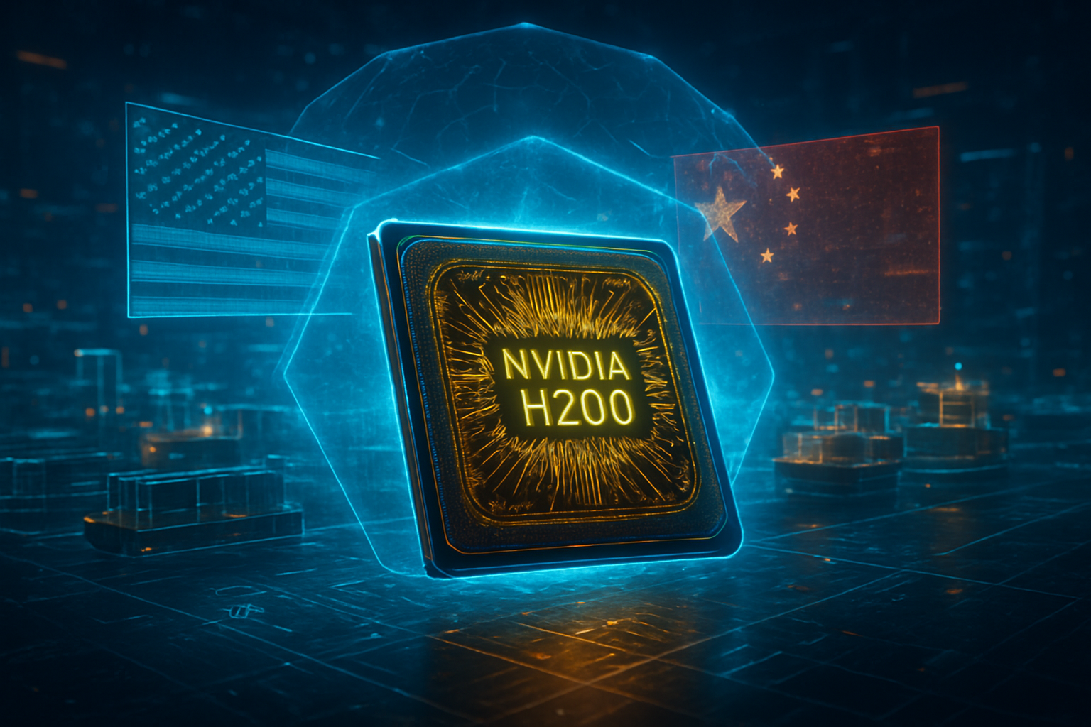
The market implications of these HVM milestones are profound. For years, the AI revolution led by Microsoft (Nasdaq: MSFT) and Alphabet (Nasdaq: GOOGL) was bottlenecked by a single point of failure: the Taiwan Strait. By January 2026, that bottleneck has been partially bypassed. Leading-edge AI startups now have the option to secure "Sovereign AI" capacity—chips manufactured entirely on U.S. soil—a requirement that is increasingly becoming standard in Department of Defense and high-security enterprise contracts.
Which companies stand to benefit most? Intel Foundry is the clear winner in the near term. By opening its 18A node to third-party customers and securing a 9.9% equity stake from the U.S. government as part of a "national champion" model, Intel has transformed from a struggling IDM into a formidable domestic foundry rival to TSMC. Conversely, TSMC has utilized its $6.6 billion in CHIPS Act grants to solidify its relationship with its largest U.S. customers, proving it can successfully replicate its legendary "Taiwan Ecosystem" in the harsh climate of the American Southwest.
However, the transition is not without friction. Industry analysts at Nomura and SEMI note that U.S.-made chips currently carry a 20–30% "resiliency premium" due to higher labor and operational costs. While the $30 billion in subsidies has offset initial capital expenditures, the long-term market positioning of these fabs will depend on whether the U.S. government introduces further protectionist measures, such as the widely discussed 100% tariff on mature-node legacy chips from non-allied nations, to ensure the new mega-fabs remain price-competitive.
The Global Chessboard: A New AI Reality
The broader significance of the CHIPS Act execution cannot be overstated. We are witnessing the first successful "industrial policy" initiative in the U.S. in recent history. In 2022, the U.S. produced 0% of the world’s most advanced logic chips; by the close of 2025, that number has climbed to 15%. This shift fits into a wider trend of "techno-nationalism," where AI hardware is viewed not just as a commodity, but as the foundational layer of national power.
Comparison to previous milestones, like the 1950s interstate highway system or the 1960s Space Race, are frequent among policy experts. Yet, the semiconductor race is arguably more complex. The potential concerns center on "subsidy addiction." If the $30 billion in funding is not followed by sustained private investment and a robust talent pipeline—Arizona alone faces a 3,000-engineer shortfall this year—the mega-fabs risk becoming "white elephants" that require perpetual government lifelines.
Furthermore, the environmental impact of these facilities has sparked local debates. The Phoenix mega-fabs consume millions of gallons of water daily, a challenge that has forced Intel and TSMC to pioneer world-leading water reclamation technologies that recycle over 90% of their intake. These environmental breakthroughs are becoming as essential to the semiconductor industry as the lithography itself.
The Horizon: 2nm and Beyond
Looking forward to the remainder of 2026 and 2027, the focus shifts from "production" to "scaling." Samsung’s Taylor, Texas facility is slated to begin its trial runs for 2nm production in late 2026, aiming to steal the lead for next-generation AI processors used in autonomous vehicles and humanoid robotics. Meanwhile, TSMC is already breaking ground on its third Phoenix fab, which is designated for the 2nm era by 2028.
The next major challenge will be the "packaging gap." While the U.S. has successfully re-shored the making of chips, the assembly and packaging of those chips still largely occur in Malaysia, Vietnam, and Taiwan. Experts predict that the next phase of CHIPS Act funding—or a potential "CHIPS 2.0" bill—will focus almost exclusively on advanced back-end packaging to ensure that a chip never has to leave U.S. soil from sand to server.
Summary: A Historic Pivot for the Industry
The early 2026 HVM milestones in Arizona, Oregon, and the construction progress in Ohio represent a historic pivot in the story of artificial intelligence. The execution of the CHIPS Act has moved from a legislative gamble to an operational reality. We have entered an era where "Made in America" is no longer a slogan for heavy machinery, but a standard for the most sophisticated nanostructures ever built by humanity.
As we watch the first 18A wafers roll off the line in Ocotillo, the takeaway is clear: the U.S. has successfully bought its way back into the semiconductor game. The long-term impact will be measured in the stability of the AI market and the security of the digital world. For the coming months, keep a close eye on yield rates and customer announcements; the hardware that will power the 2030s is being born today in the American heartland.
This content is intended for informational purposes only and represents analysis of current AI developments.
TokenRing AI delivers enterprise-grade solutions for multi-agent AI workflow orchestration, AI-powered development tools, and seamless remote collaboration platforms.
For more information, visit https://www.tokenring.ai/.