As of January 2026, the scorched earth of Phoenix, Arizona, has officially become the most strategically significant piece of real estate in the global technology sector. Taiwan Semiconductor Manufacturing Company (NYSE: TSM), the world’s most advanced chipmaker, has successfully transitioned its Arizona "Gigafab" complex from a contentious multi-billion dollar bet into a high-yield production powerhouse. Following a landmark January 15, 2026, earnings call, TSMC confirmed it has expanded its total committed investment in the site to a staggering $165 billion, with long-term internal projections suggesting a decade-long expansion toward a $465 billion 12-fab cluster.
The immediate significance of this development cannot be overstated: for the first time in the history of the modern artificial intelligence era, the most complex silicon in the world is being forged at scale on American soil. With Fab 1 (Phase 21) now reaching high-volume manufacturing (HVM) for 4nm and 5nm nodes, the "Made in USA" label is no longer a symbolic gesture but a logistical reality for the hardware that powers the world's most advanced Large Language Models. This milestone marks the definitive end of the "efficiency-only" era of semiconductor manufacturing, giving way to a new paradigm of supply chain resilience and geopolitical security.
The Technical Blueprint: Reaching Yield Parity in the Desert
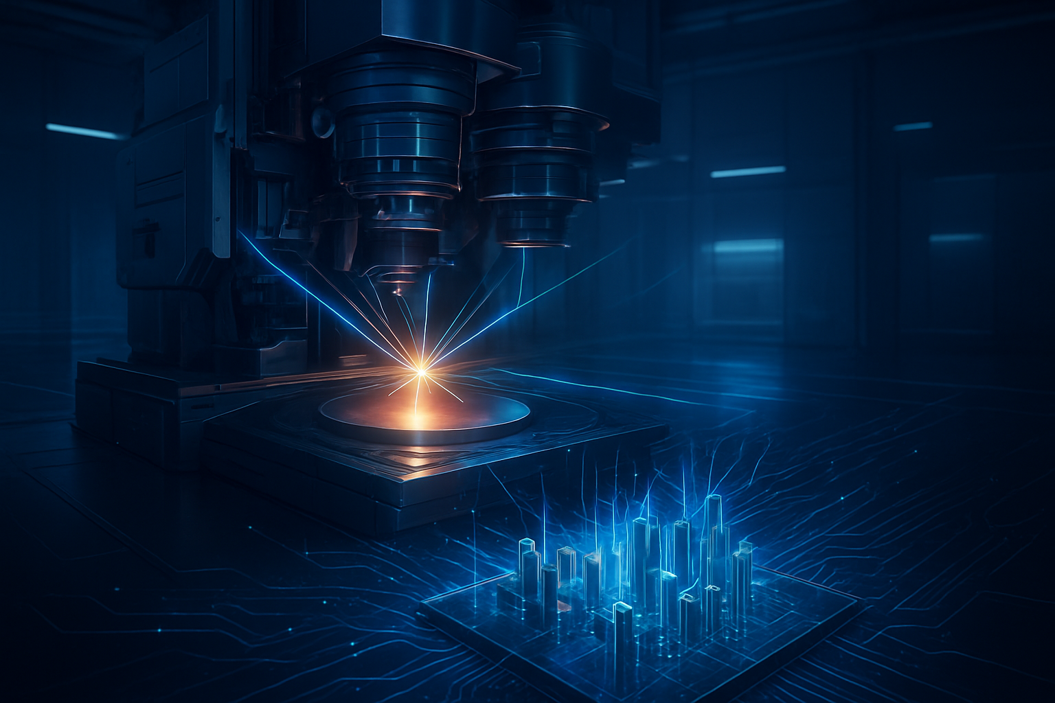
Technical specifications from the Arizona site as of early 2026 indicate a performance level that many industry experts thought impossible just two years ago. Fab 1, utilizing the N4P (4nm) process, has reached a silicon yield of 88–92%, effectively matching the efficiency of TSMC’s flagship "GigaFabs" in Tainan. This achievement silences long-standing skepticism regarding the compatibility of Taiwanese high-precision manufacturing with U.S. labor and environmental conditions. Meanwhile, construction on Fab 2 has been accelerated to meet "insatiable" demand for 3nm (N3) technology, with equipment move-in currently underway and mass production scheduled for the second half of 2027.
Beyond the logic gates, the most critical technical advancement in Arizona is the 2026 groundbreaking of the AP1 and AP2 facilities—TSMC’s dedicated domestic advanced packaging plants. Previously, even "U.S.-made" chips had to be shipped back to Taiwan for Chip-on-Wafer-on-Substrate (CoWoS) packaging, creating a "logistical loop" that critics argued compromised the very security the Arizona project was meant to provide. By late 2026, the Arizona cluster will offer a "turnkey" solution, where a raw silicon wafer enters the Phoenix site and emerges as a fully packaged, ready-to-deploy AI accelerator.
The technical gap between TSMC and its competitors remains a focal point of the industry. While Intel Corporation (NASDAQ: INTC) has successfully launched its 18A (1.8nm) node at its own Arizona and Ohio facilities, TSMC continues to lead in commercial yield and customer confidence. Samsung Electronics (KSE: 005930) has pivoted its Taylor, Texas, strategy to focus exclusively on 2nm (SF2) by late 2026, but the sheer scale of the TSMC Arizona cluster—which now includes plans for Fab 3 to handle 2nm and the future "A16" angstrom-class nodes—keeps the Taiwanese giant firmly in the dominant position for AI-grade silicon.
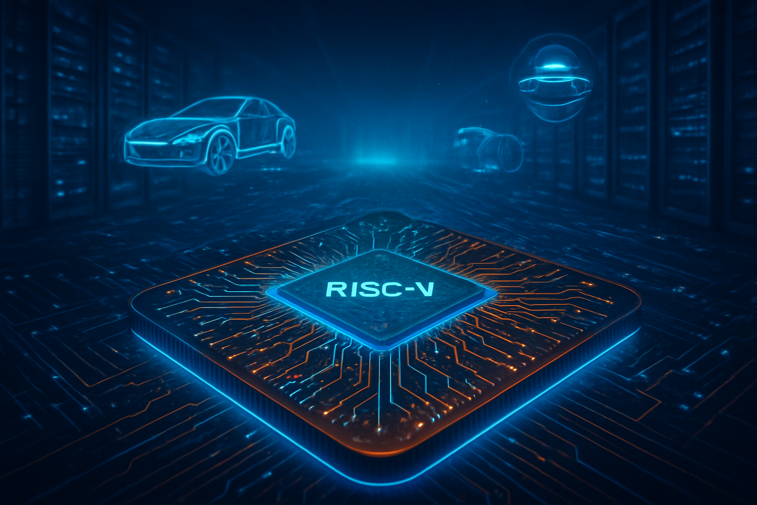
The Power Players: Why NVIDIA and Apple are Anchoring in the Desert
In a historic market realignment confirmed this month, NVIDIA (NASDAQ: NVDA) has officially overtaken Apple (NASDAQ: AAPL) as TSMC’s largest customer by revenue. This shift is vividly apparent in Arizona, where the Phoenix fab has become the primary production hub for NVIDIA’s Blackwell-series GPUs, including the B200 and B300 accelerators. For NVIDIA, the Arizona Gigafab is more than a factory; it is a hedge against escalating tensions in the Taiwan Strait, ensuring that the critical hardware required for global AI workloads remains shielded from regional conflict.
Apple, while now the second-largest customer, remains a primary anchor for the site’s 3nm and 2nm future. The Cupertino giant was the first to utilize Fab 1 for its A-series and M-series chips, and is reportedly competing aggressively with Advanced Micro Devices (NASDAQ: AMD) for early capacity in the upcoming Fab 2. This surge in demand has forced other tech giants like Microsoft (NASDAQ: MSFT) and Meta (NASDAQ: META) to negotiate their own long-term supply agreements directly with the Arizona site, rather than relying on global allocations from Taiwan.
The market positioning is clear: TSMC Arizona has become the "high-rent district" of the semiconductor world. While manufacturing costs in the U.S. remain roughly 10% higher than in Taiwan—largely due to a 200% premium on skilled labor—the strategic advantage of geographic proximity to Silicon Valley and the political stability of the U.S. has turned a potential cost-burden into a premium service. For companies like Qualcomm (NASDAQ: QCOM) and Amazon (NASDAQ: AMZN), having a "domestic source" is increasingly viewed as a requirement for government contracts and infrastructure security, further solidifying TSMC’s dominant 75% market share in advanced nodes.
Geopolitical Resilience: The $6.6 Billion CHIPS Act Catalyst
The wider significance of the Arizona Gigafab is inextricably linked to the landmark US-Taiwan Trade Agreement signed in early January 2026. This pact reduced technology export tariffs from 20% to 15%, a "preferential treatment" designed to reward the massive onshoring of fabrication. This agreement acts as a diplomatic shield, fostering a "40% Supply Chain" goal where U.S. officials aim to have 40% of Taiwan’s critical chip supply chain physically located on American soil by 2029.
The U.S. government’s role, through the CHIPS and Science Act, has been the primary engine for this acceleration. TSMC has already begun receiving its first major tranches of the $6.6 billion in direct grants and $5 billion in federal loans. Furthermore, the company is expected to claim nearly $8 billion in investment tax credits by the end of 2026. However, this funding comes with strings: TSMC is currently navigating the "upside sharing" clause, which requires it to return a portion of its Arizona profits to the U.S. government if returns exceed specific projections—a likely scenario given the current AI boom.
Despite the triumphs, the project has faced significant headwinds. A "99% profit collapse" reported at the Arizona site in late 2025 followed a catastrophic gas supplier outage, highlighting that the local supply chain ecosystem is still maturing. The talent shortage remains the most persistent concern, with TSMC continuing to import thousands of engineers from its Hsinchu headquarters to bridge the gap until local training programs at Arizona State University and other institutions can supply a steady flow of specialized technicians.
Future Horizons: The 12-Fab Vision and the 2nm Transition
Looking toward 2030, the Arizona project is poised for an expansion that would dwarf any other industrial project in U.S. history. Internal TSMC documents and January 2026 industry reports suggest the Phoenix site could eventually house 12 fabs, representing a total investment of nearly half a trillion dollars. This roadmap includes the transition to 2nm (N2) production at Fab 3 by 2028, and the introduction of High-NA EUV (Extreme Ultraviolet) lithography machines—the most precise tools ever made—into the Arizona desert by 2027.
The next critical milestone for investors and analysts to watch is the resolution of the U.S.-Taiwan double-taxation pact. Experts predict that once this final legislative hurdle is cleared, it will trigger a secondary wave of investment from dozens of TSMC’s key suppliers (such as chemical and material providers), creating a self-sustaining "Silicon Desert" ecosystem. Furthermore, the integration of AI-powered automation within the fabs themselves is expected to continue narrowing the cost gap between U.S. and Asian manufacturing, potentially making the Arizona site more profitable than its Taiwanese counterparts by the turn of the decade.
A Legacy in Silicon
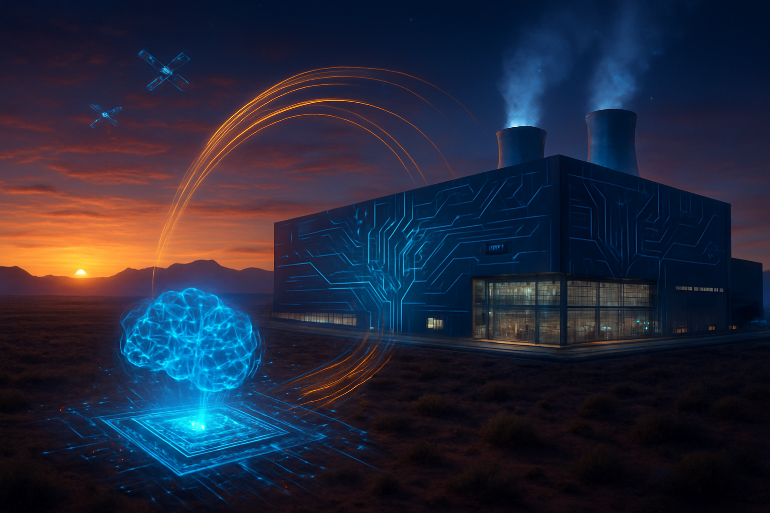
The operational success of TSMC's Arizona Gigafab in 2026 represents a historic pivot in the story of human technology. It is a testament to the fact that with enough capital, political will, and engineering brilliance, the world’s most complex supply chain can be re-anchored. For the AI industry, this development provides the physical foundation for the next decade of growth, ensuring that the "brains" of the digital revolution are manufactured in a stable, secure, and increasingly integrated global environment.
The coming months will be defined by the rapid ramp-up of Fab 2 and the first full-scale integration of the Arizona-based advanced packaging plants. As the AI arms race intensifies, the desert outside Phoenix is no longer just a construction site; it is the heartbeat of the modern world.
This content is intended for informational purposes only and represents analysis of current AI developments.
TokenRing AI delivers enterprise-grade solutions for multi-agent AI workflow orchestration, AI-powered development tools, and seamless remote collaboration platforms.
For more information, visit https://www.tokenring.ai/.