In an era defined by the frantic release of iterative chatbots and commercial AI wrappers, Safe Superintelligence Inc. (SSI) stands as a stark, multibillion-dollar anomaly. Founded by Ilya Sutzkever, the former Chief Scientist of OpenAI, SSI has eschewed the traditional Silicon Valley trajectory of "move fast and break things" in favor of a singular, monolithic goal: the development of a superintelligent system that is safe by design. Since its high-profile launch in mid-2024, the company has transformed from a provocative concept into a powerhouse of elite research, commanding a staggering $32 billion valuation as of January 2026 without having released a single public product.
The significance of SSI lies in its refusal to participate in the "product-first" arms race. While competitors like OpenAI and Anthropic have focused on scaling user bases and securing enterprise contracts, SSI has operated in a state of "scaling in peace." This strategy, championed by Sutzkever, posits that the path to true Artificial General Intelligence (AGI) requires an environment insulated from the quarterly earnings pressure of tech giants like Microsoft (NASDAQ: MSFT) or the immediate demand for consumer-facing features. By focusing exclusively on the technical hurdles of alignment and reasoning, SSI is attempting to leapfrog the "data wall" that many experts believe is currently slowing the progress of traditional Large Language Models (LLMs).
The Technical Rebellion: Scaling Reasoning Over Raw Data
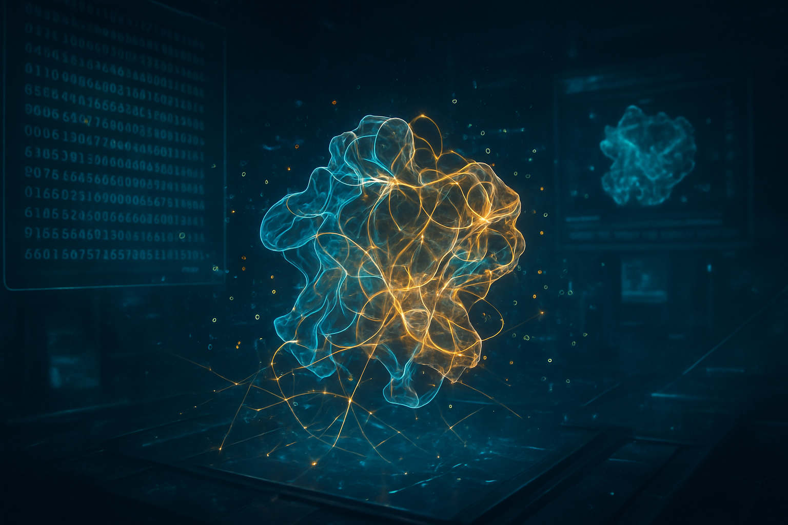
Technically, SSI represents a pivot away from the brute-force scaling laws that dominated the early 2020s. While the industry previously focused on feeding more raw internet data into increasingly massive clusters of Nvidia (NASDAQ: NVDA) GPUs, SSI has moved toward "conceptual alignment" and synthetic reasoning. Under the leadership of Sutzkever and President Daniel Levy, the company has reportedly prioritized the development of models that can verify their own logic and internalize safety constraints at a fundamental architectural level, rather than through post-training fine-tuning. This "Safety-First" architecture is designed to prevent the emergent unpredictable behaviors that have plagued earlier iterations of AGI research.
Initial reactions from the AI research community have been a mix of reverence and skepticism. Leading researchers from academic institutions have praised SSI for returning to "pure" science, noting that the company's team—estimated at 50 to 70 "cracked" engineers across Palo Alto and Tel Aviv—is perhaps the highest-density collection of AI talent in history. However, critics argue that the lack of iterative deployment makes it difficult to stress-test safety measures in real-world scenarios. Unlike the feedback loops generated by millions of ChatGPT users, SSI relies on internal adversarial benchmarks, a method that some fear could lead to a "black box" development cycle where flaws are only discovered once the system is too powerful to contain.
Shifting the Power Dynamics of Silicon Valley
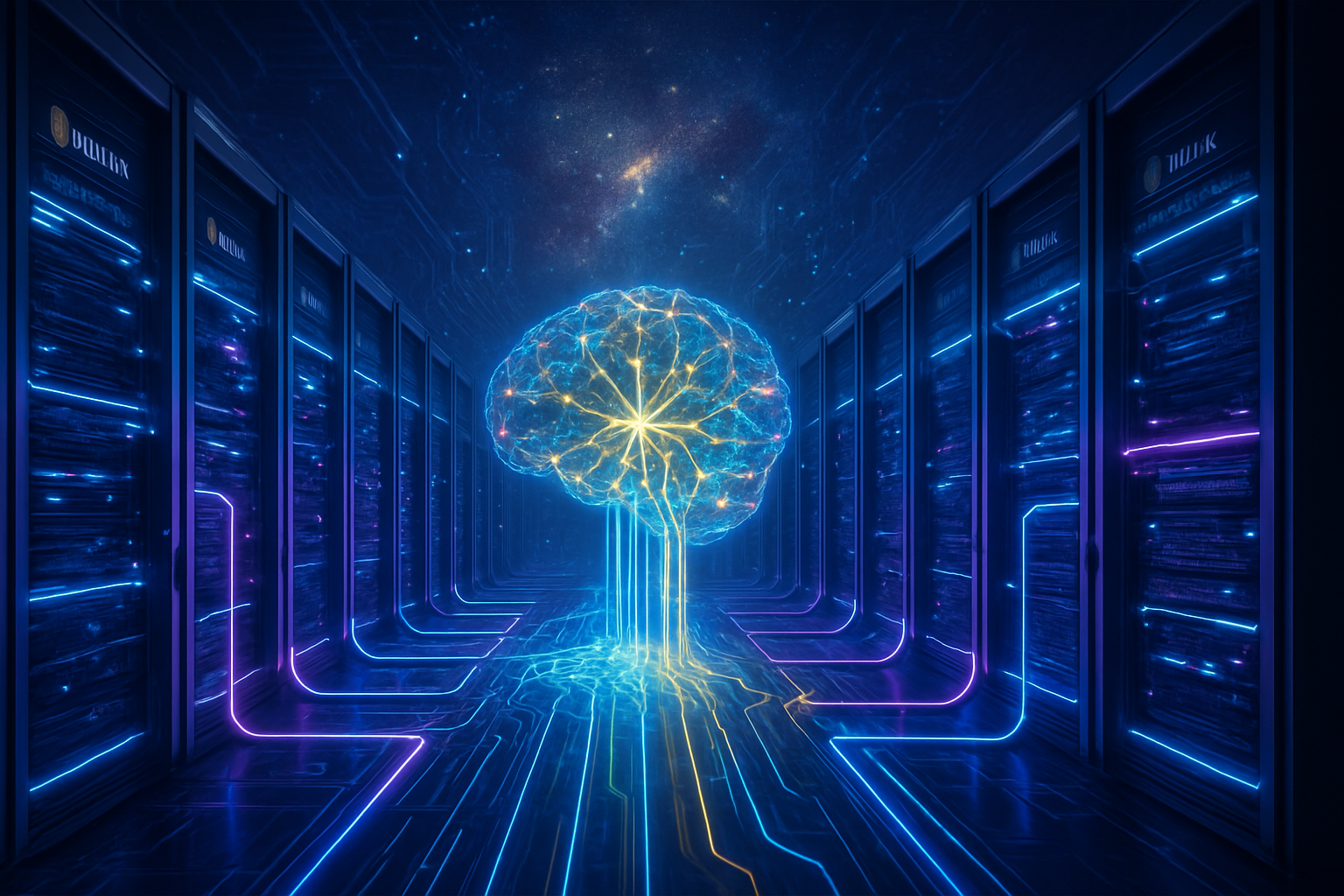
The emergence of SSI has sent ripples through the corporate landscape, forcing tech giants to reconsider their own R&D structures. Alphabet (NASDAQ: GOOGL), which serves as SSI’s primary infrastructure provider through Google Cloud’s TPU clusters, finds itself in a strategic paradox: it is fueling a potential competitor while benefiting from the massive compute spend. Meanwhile, the talent war has intensified. The mid-2025 departure of SSI co-founder Daniel Gross to join Meta (NASDAQ: META) underscored the high stakes, as Mark Zuckerberg’s firm reportedly attempted an outright acquisition of SSI to bolster its own superintelligence ambitions.
For startups, SSI serves as a new model for "deep tech" financing. By raising over $3 billion in total funding from heavyweights like Andreessen Horowitz, Sequoia Capital, and Greenoaks Capital without a revenue model, SSI has proven that venture capital still has an appetite for high-risk, long-horizon moonshots. This has pressured other labs to justify their commercial distractions. If SSI succeeds in reaching superintelligence first, the existing product lines of many AI companies—from coding assistants to customer service bots—could be rendered obsolete overnight by a system that possesses vastly superior general reasoning capabilities.
A Moral Compass in the Age of Acceleration
The wider significance of SSI is rooted in the existential debate over AI safety. By making "Safe" the first word in its name, the company has successfully reframed the AGI conversation from "when" to "how." This fits into a broader trend where the "doomer" vs. "effective accelerationist" (e-acc) divide has stabilized into a more nuanced discussion about institutional design. SSI’s existence is a direct critique of the "move fast" culture at OpenAI, suggesting that the current commercial structures are fundamentally ill-equipped to handle the transition to superintelligence without risking catastrophic misalignment.
However, the "stealth" nature of SSI has raised concerns about transparency and democratic oversight. As the company scales its compute power—rumored to be among the largest private clusters in the world—the lack of public-facing researchers or open-source contributions creates a "fortress of solitude" effect. Comparisons have been made to the Manhattan Project; while the goal is the betterment of humanity, the development is happening behind closed doors, protected by extreme operational security including Faraday-caged interview rooms. The concern remains that a private corporation, however well-intentioned, holds the keys to a technology that could redefine the human experience.
The Path Forward: Breaking the Data Wall
Looking toward the near-term future, SSI is expected to remain in stealth mode while it attempts to solve the "reasoning bottleneck." Experts predict that 2026 will be the year SSI reveals whether its focus on synthetic reasoning and specialized Google TPUs can actually outperform the massive, data-hungry clusters of its rivals. If the company can demonstrate a model that learns more efficiently from less data—essentially "thinking" its way to intelligence—it will validate Sutzkever's hypothesis and likely trigger another massive wave of capital flight toward safety-centric labs.
The primary challenge remains the "deployment gap." As SSI continues to scale, the pressure to prove its safety benchmarks will grow. We may see the company begin to engage with international regulatory bodies or "red-teaming" consortiums to validate its progress without a full commercial launch. There is also the lingering question of a business model; while the $32 billion valuation suggests investor patience, any sign that AGI is further than a decade away could force SSI to pivot toward high-end scientific applications, such as autonomous drug discovery or materials science, to sustain its burn rate.
Conclusion: The Ultimate High-Stakes Experiment
The launch and subsequent ascent of Safe Superintelligence Inc. mark a pivotal moment in the history of technology. It is a gamble on the idea that the most important invention in human history cannot be built in the back of a retail shop. By stripping away the distractions of product cycles and profit margins, Ilya Sutzkever has created a laboratory dedicated to the purest form of the AI challenge. Whether this isolation leads to a breakthrough in human-aligned intelligence or becomes a cautionary tale of "ivory tower" research remains to be seen.
As we move through 2026, the industry will be watching SSI’s recruitment patterns and compute acquisitions for clues about their progress. The company’s success would not only redefine our technical capabilities but also prove that a mission-driven, non-commercial approach can survive in the world’s most competitive industry. For now, SSI remains the most expensive and most important "stealth" project in the world, a quiet giant waiting for the right moment to speak.
This content is intended for informational purposes only and represents analysis of current AI developments.
TokenRing AI delivers enterprise-grade solutions for multi-agent AI workflow orchestration, AI-powered development tools, and seamless remote collaboration platforms.
For more information, visit https://www.tokenring.ai/.