CUPERTINO, CA — Apple (NASDAQ: AAPL) has officially ushered in what it calls the "Intelligence Era" with the full-scale launch of Apple Intelligence across its latest software ecosystem. While the transition from iOS 18 to the current iOS 26 numbering system initially surprised the industry, the milestone commonly referred to as the "iOS 20" generational leap has finally arrived, bringing a sophisticated, privacy-first AI architecture to hundreds of millions of users. This release represents a fundamental shift in computing, moving away from a collection of apps and toward an integrated, agent-based operating system powered by on-device foundation models.
The significance of this launch lies in Apple’s unique approach to generative AI: a hybrid architecture that prioritizes local processing while selectively utilizing high-capacity cloud models. By launching the highly anticipated Foundation Models API, Apple is now allowing third-party developers to tap into the same 3-billion parameter on-device models that power Siri, effectively commoditizing high-end AI features for the entire App Store ecosystem.
Technical Mastery on the Edge: The 3-Billion Parameter Powerhouse
The technical backbone of this update is the Apple Foundation Model (AFM), a proprietary transformer model specifically optimized for the Neural Engine in the A19 and A20 Pro chips. Unlike cloud-heavy competitors, Apple’s model utilizes advanced 2-bit and 4-bit quantization techniques to run locally with sub-second latency. This allows for complex tasks—such as text generation, summarization, and sentiment analysis—to occur entirely on the device without the need for an internet connection. Initial benchmarks from the AI research community suggest that while the 3B model lacks the broad "world knowledge" of larger LLMs, its efficiency in task-specific reasoning and "On-Screen Awareness" is unrivaled in the mobile space.
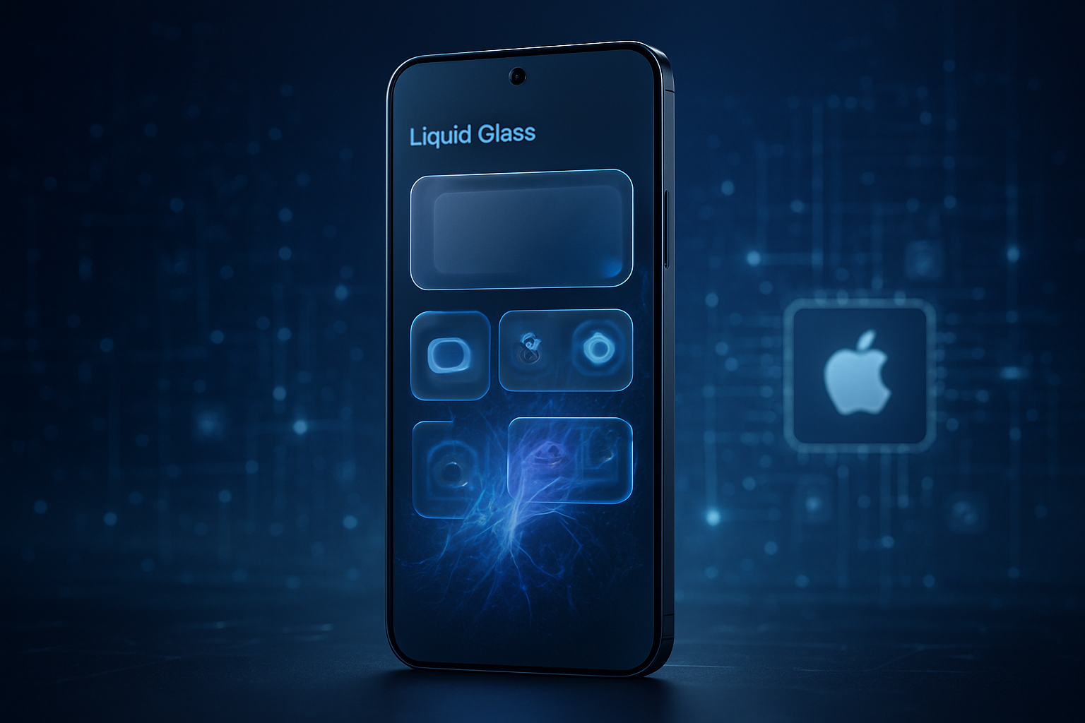
The launch also introduces the "Liquid Glass" design system, a new UI paradigm where interface elements react dynamically to the AI's processing. For example, when a user asks Siri to "send the document I was looking at to Sarah," the OS uses computer vision and semantic understanding to identify the open file and the correct contact, visually highlighting the elements as they are moved between apps. Experts have noted that this "semantic intent" layer is what truly differentiates Apple from existing "chatbot" approaches; rather than just talking to a box, users are interacting with a system that understands the context of their digital lives.
Market Disruptions: The End of the "AI Wrapper" Era
The release of the Foundation Models API has sent shockwaves through the tech industry, particularly affecting AI startups. By offering "Zero-Cost Inference," Apple has effectively neutralized the business models of many "wrapper" apps—services that previously charged users for simple AI tasks like PDF summarization or email drafting. Developers can now implement these features with as few as three lines of Swift code, leveraging the on-device hardware rather than paying for expensive tokens from providers like OpenAI or Anthropic.
Strategically, Apple’s partnership with Alphabet Inc. (NASDAQ: GOOGL) to integrate Google Gemini as a "world knowledge" fallback has redefined the competitive landscape. By positioning Gemini as an opt-in tool for high-level reasoning, Apple (NASDAQ: AAPL) has successfully maintained its role as the primary interface for the user, while offloading the most computationally expensive and "hallucination-prone" tasks to Google’s infrastructure. This positioning strengthens Apple's market power, as it remains the "curator" of the AI experience, deciding which third-party models get access to its massive user base.
A New Standard for Privacy: The Private Cloud Compute Model
Perhaps the most significant aspect of the launch is Apple’s commitment to "Private Cloud Compute" (PCC). Recognizing that some tasks remain too complex for even the A20 chip, Apple has deployed a global network of "Baltra" servers—custom Apple Silicon-based hardware designed as stateless enclaves. When a request is too heavy for the device, it is sent to PCC, where the data is processed without ever being stored or accessible to Apple employees.
This architecture addresses the primary concern of the modern AI landscape: the trade-off between power and privacy. Unlike traditional cloud AI, where user prompts often become training data, Apple's system is built for "verifiable privacy." Independent security researchers have already begun auditing the PCC source code, a move that has been praised by privacy advocates as a landmark in corporate transparency. This shift forces competitors like Microsoft (NASDAQ: MSFT) and Meta (NASDAQ: META) to justify their own data collection practices as the "Apple standard" becomes the new baseline for consumer expectations.
The Horizon: Siri 2.0 and the Road to iOS 27
Looking ahead, the near-term roadmap for Apple Intelligence is focused on the "Siri 2.0" rollout, currently in beta for the iOS 26.4 cycle. This update is expected to fully integrate the "Agentic AI" capabilities of the Foundation Models API, allowing Siri to execute multi-step actions across dozens of third-party apps autonomously. For instance, a user could soon say, "Book a table for four at a nearby Italian place and add it to the shared family calendar," and the system will handle the reservation, confirmation, and scheduling without further input.
Predicting the next major milestone, experts anticipate the launch of the iPhone 16e in early spring, which will serve as the entry-point device for these AI features. Challenges remain, particularly regarding the "aggressive guardrails" Apple has placed on its models. Developers have noted that the system's safety layers can sometimes be over-cautious, refusing to summarize certain types of content. Apple will need to fine-tune these parameters to ensure the AI remains helpful without becoming frustratingly restrictive.
Conclusion: A Definitive Turning Point in AI History
The launch of Apple Intelligence and the transition into the iOS 20/26 era marks the moment AI moved from a novelty to a fundamental utility. By prioritizing on-device processing and empowering developers through the Foundation Models API, Apple has created a scalable, private, and cost-effective ecosystem that its competitors will likely be chasing for years.
Key takeaways from this launch include the normalization of edge-based AI, the rise of the "agentic" interface, and a renewed industry focus on verifiable privacy. As we look toward the upcoming WWDC and the eventual transition to iOS 27, the tech world will be watching closely to see how the "Liquid Glass" experience evolves and whether the partnership with Google remains a cornerstone of Apple’s cloud strategy. For now, one thing is certain: the era of the "smart" smartphone has officially been replaced by the era of the "intelligent" companion.
This content is intended for informational purposes only and represents analysis of current AI developments.
TokenRing AI delivers enterprise-grade solutions for multi-agent AI workflow orchestration, AI-powered development tools, and seamless remote collaboration platforms.
For more information, visit https://www.tokenring.ai/.