As the global artificial intelligence race shifts its focus from massive data centers to the "intelligent edge," a new hardware paradigm is emerging to challenge the dominance of traditional silicon. In a major move to bridge the widening gap between cutting-edge research and industrial application, neuromorphic chipmaker Innatera has announced a landmark partnership with VLSI Expert to train the next generation of semiconductor engineers. This collaboration aims to formalize the study of brain-mimicking architectures, ensuring a steady pipeline of talent capable of designing the ultra-low-power, event-driven systems that will define the next decade of "always-on" AI.
The partnership arrives at a critical juncture for the semiconductor industry, directly addressing two of the most pressing challenges in technology today: the technical plateau of traditional Von Neumann architectures (Item 15: Neuromorphic Computing) and the crippling global shortage of specialized engineering expertise (Item 25: The Talent War). By integrating Innatera’s proprietary Spiking Neural Processor (SNP) technology into VLSI Expert’s worldwide training modules, the two companies are positioning themselves at the vanguard of a shift toward "Ambient Intelligence"—where sensors can see, hear, and feel with a power budget smaller than a single grain of rice.
The Pulse of Innovation: Inside the Spiking Neural Processor
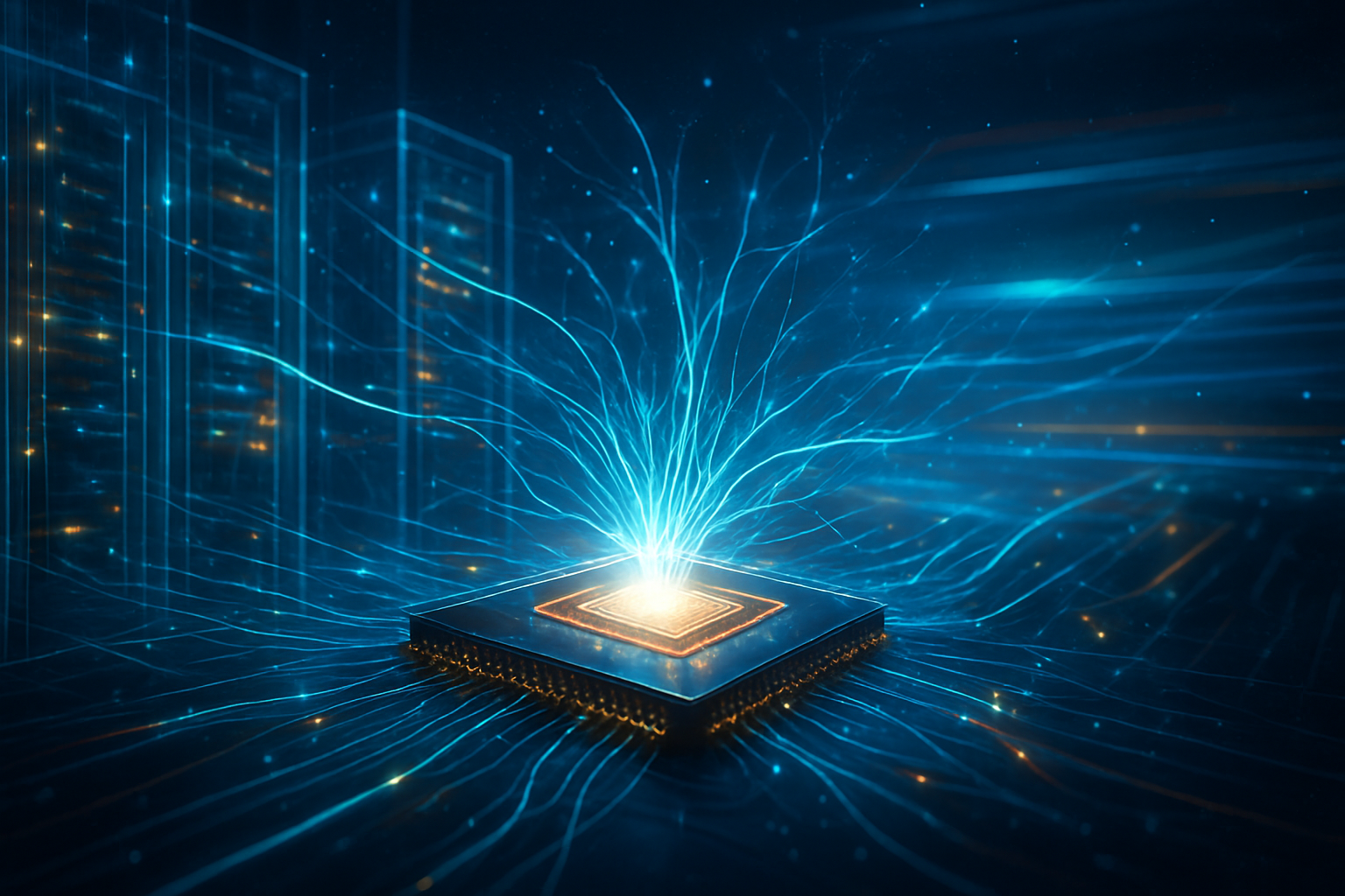
At the heart of this development is Innatera’s Pulsar chip, a revolutionary piece of hardware that abandons the continuous data streams used by companies like NVIDIA Corporation (NASDAQ: NVDA) in favor of "spikes." Much like the human brain, the Pulsar processor only consumes energy when it detects a change in its environment, such as a specific sound pattern or a sudden movement. This event-driven approach allows the chip to operate within a microwatt power envelope, often achieving 100 times lower latency and 500 times greater energy efficiency than conventional digital signal processors or edge-AI microcontrollers.
Technically, the Pulsar architecture is a hybrid marvel. It combines an analog-mixed signal Spiking Neural Network (SNN) engine with a digital RISC-V CPU and a dedicated Convolutional Neural Network (CNN) accelerator. This allows developers to utilize the high-speed efficiency of neuromorphic "spikes" while maintaining compatibility with traditional AI frameworks. The recently unveiled 2026 iterations of the platform include integrated power management and an FFT/IFFT engine, specifically designed to process complex frequency-domain data for industrial sensors and wearable medical devices without ever needing to wake up a primary system-on-chip (SoC).
Unlike previous attempts at neuromorphic computing that remained confined to academic labs, Innatera’s platform is designed for mass-market production. The technical leap here isn't just in the energy savings; it is in the "sparsity" of the computation. By processing only the most relevant "events" in a data stream, the SNP ignores 99% of the noise that typically drains the batteries of mobile and IoT devices. This differs fundamentally from traditional architectures that must constantly cycle through data, regardless of whether that data contains meaningful information.
Initial reactions from the AI research community have been overwhelmingly positive, with many experts noting that the biggest hurdle for neuromorphic adoption hasn't been the hardware, but the software stack and developer familiarity. Innatera’s Talamo SDK, which is a core component of the new VLSI Expert training curriculum, bridges this gap by allowing engineers to map workloads from familiar environments like PyTorch and TensorFlow directly onto spiking hardware. This "democratization" of neuromorphic design is seen by many as the "missing link" for edge AI.
Strategic Maneuvers in the Silicon Trenches
The strategic partnership between Innatera and VLSI Expert has sent ripples through the corporate landscape, particularly among tech giants like Intel Corporation (NASDAQ: INTC) and International Business Machines Corporation (NYSE: IBM). Intel has long championed neuromorphic research through its Loihi chips, and IBM has pushed the boundaries with its NorthPole architecture. However, Innatera’s focus on the sub-milliwatt power range targets a highly lucrative "ultra-low power" niche that is vital for the consumer electronics and industrial IoT sectors, potentially disrupting the market positioning of established edge-AI players.
Competitive implications are also mounting for specialized firms like BrainChip Holdings Ltd (ASX: BRN). While BrainChip has found success with its Akida platform in automotive and aerospace sectors, the Innatera-VLSI Expert alliance focuses heavily on the "Talent War" by upskilling thousands of engineers in India and the United States. By securing the minds of future designers, Innatera is effectively creating a "moat" built on human capital. If an entire generation of VLSI engineers is trained on the Pulsar architecture, Innatera becomes the default choice for any startup or enterprise building "always-on" sensing products.
Major AI labs and semiconductor firms stand to benefit immensely from this initiative. As the demand for privacy-preserving, local AI processing grows, companies that can deploy neuromorphic-ready teams will have a significant time-to-market advantage. We are seeing a shift where strategic advantage is no longer just about who has the fastest chip, but who has the workforce capable of programming complex, asynchronous systems. This partnership could force other major players to launch similar educational initiatives to avoid being left behind in the specialized talent race.
Furthermore, the disruption extends to existing products in the "smart home" and "wearable" categories. Current devices that rely on cloud-based voice or gesture recognition face latency and privacy hurdles. Innatera’s push into the training sector suggests a future where localized, "dumb" sensors are replaced by autonomous, "neuromorphic" ones. This shift could marginalize existing low-power microcontroller lines that lack specialized AI acceleration, forcing a consolidation in the mid-tier semiconductor market.
Addressing the Talent War and the Neuromorphic Horizon
The broader significance of this training initiative cannot be overstated. It directly connects to Item 15 and Item 25 of our industry analysis, highlighting a pivot point in the AI landscape. For years, the industry has focused on "Generative AI" and "Large Language Models" running on massive power grids. However, as we enter 2026, the trend of "Ambient Intelligence" requires a different kind of breakthrough. Neuromorphic computing is the only viable path to achieving human-like perception in devices that lack a constant power source.
The "Talent War" described in Item 25 is currently the single greatest bottleneck in the semiconductor industry. Reports from late 2025 indicated a shortage of over one million semiconductor specialists globally. Neuromorphic engineering is even more specialized, requiring knowledge of biology, physics, and computer science. By formalizing this curriculum, Innatera and VLSI Expert are treating "designing intelligence" as a separate discipline from traditional "chip design." This milestone mirrors the early days of GPU development, where the creation of CUDA by NVIDIA transformed how software interacted with hardware.
However, the transition is not without concerns. The move toward brain-mimicking chips raises questions about the "black box" nature of AI. As these chips become more autonomous and capable of real-time learning at the edge, ensuring they remain predictable and secure is paramount. Critics also point out that while neuromorphic chips are efficient, the ecosystem for "event-based" software is still in its infancy compared to the decades of optimization poured into traditional digital logic.
Despite these challenges, the comparison to previous AI milestones is striking. Just as the transition from CPUs to GPUs enabled the deep learning revolution of the 2010s, the transition to neuromorphic SNP architectures is poised to enable the "Sensory AI" revolution of the late 2020s. This is the moment where AI leaves the server rack and enters the physical world in a meaningful, persistent way.
The Future of Edge Intelligence: What’s Next?
In the near term, we expect to see a surge in "neuromorphic-first" consumer devices. By late 2026, it is likely that the first wave of engineers trained through the VLSI Expert program will begin delivering commercial products. These will likely include hearables with unparalleled noise cancellation, industrial sensors that can predict mechanical failure through vibration analysis alone, and medical wearables that monitor heart health with medical-grade precision for months on a single charge.
Longer-term, the applications expand into autonomous robotics and smart infrastructure. Experts predict that as neuromorphic chips become more sophisticated, they will begin to incorporate "on-chip learning," allowing devices to adapt to their specific user or environment without ever sending data to the cloud. This solves the dual problems of privacy and bandwidth that have plagued the IoT industry for a decade. The challenge remains in scaling these architectures to handle more complex reasoning tasks, but for sensing and perception, the path is clear.
The next year will be telling. We should watch for the integration of Innatera’s IP into larger SoC designs through licensing agreements, as well as the potential for a major acquisition as tech giants look to swallow up the most successful neuromorphic startups. The "Talent War" will continue to escalate, and the success of this training partnership will serve as a blueprint for how other hardware niches might solve their own labor shortages.
A New Chapter in AI History
The partnership between Innatera and VLSI Expert marks a definitive moment in AI history. It signals that neuromorphic computing has moved beyond the "hype cycle" and into the "execution phase." By focusing on the human element—the engineers who will actually build the future—these companies are addressing the most critical infrastructure of all: knowledge.
The key takeaway for 2026 is that the future of AI is not just larger models, but smarter, more efficient hardware. The significance of brain-mimicking chips lies in their ability to make intelligence invisible and ubiquitous. As we move forward, the metric for AI success will shift from "FLOPS" (Floating Point Operations Per Second) to "SOPS" (Synaptic Operations Per Second), reflecting a deeper understanding of how both biological and artificial minds actually work.
In the coming months, keep a close eye on the rollout of the Pulsar-integrated developer kits in India and the US. Their adoption rates among university labs and industrial design houses will be the primary indicator of how quickly neuromorphic computing will become the new standard for the edge. The talent war is far from over, but for the first time, we have a clear map of the battlefield.
This content is intended for informational purposes only and represents analysis of current AI developments.
TokenRing AI delivers enterprise-grade solutions for multi-agent AI workflow orchestration, AI-powered development tools, and seamless remote collaboration platforms.
For more information, visit https://www.tokenring.ai/.