Blog

  • OpenAI’s ‘Stargate’ to $830 Billion: Historic $100 Billion Funding Round Reshapes the AI Super-Cycle

    OpenAI’s ‘Stargate’ to $830 Billion: Historic $100 Billion Funding Round Reshapes the AI Super-Cycle

    OpenAI has shattered the record for private capital raises, reportedly entering the final stages of a monumental $100 billion funding round that values the artificial intelligence leader at a staggering $830 billion. This capital injection, led by a surprising alliance between Amazon (NASDAQ: AMZN), SoftBank (TYO: 9984), and existing partners like Microsoft (NASDAQ: MSFT), marks a pivotal moment in the global AI arms race. The sheer scale of the investment underscores a fundamental shift in the industry: the transition from software optimization to the massive, physical infrastructure required to sustain the next generation of artificial general intelligence (AGI).

    This unprecedented infusion of cash is not merely a balance sheet expansion; it is the fuel for "Project Stargate," OpenAI’s ambitious multi-year initiative to build a global network of AI supercomputing clusters. As the company moves toward a highly anticipated initial public offering (IPO) expected in late 2026, the $830 billion valuation positions OpenAI not just as a startup, but as a systemic pillar of the global economy, rivaling the market caps of the world's most established tech giants.

    The Architecture of AGI: Project Stargate and Technical Scaling

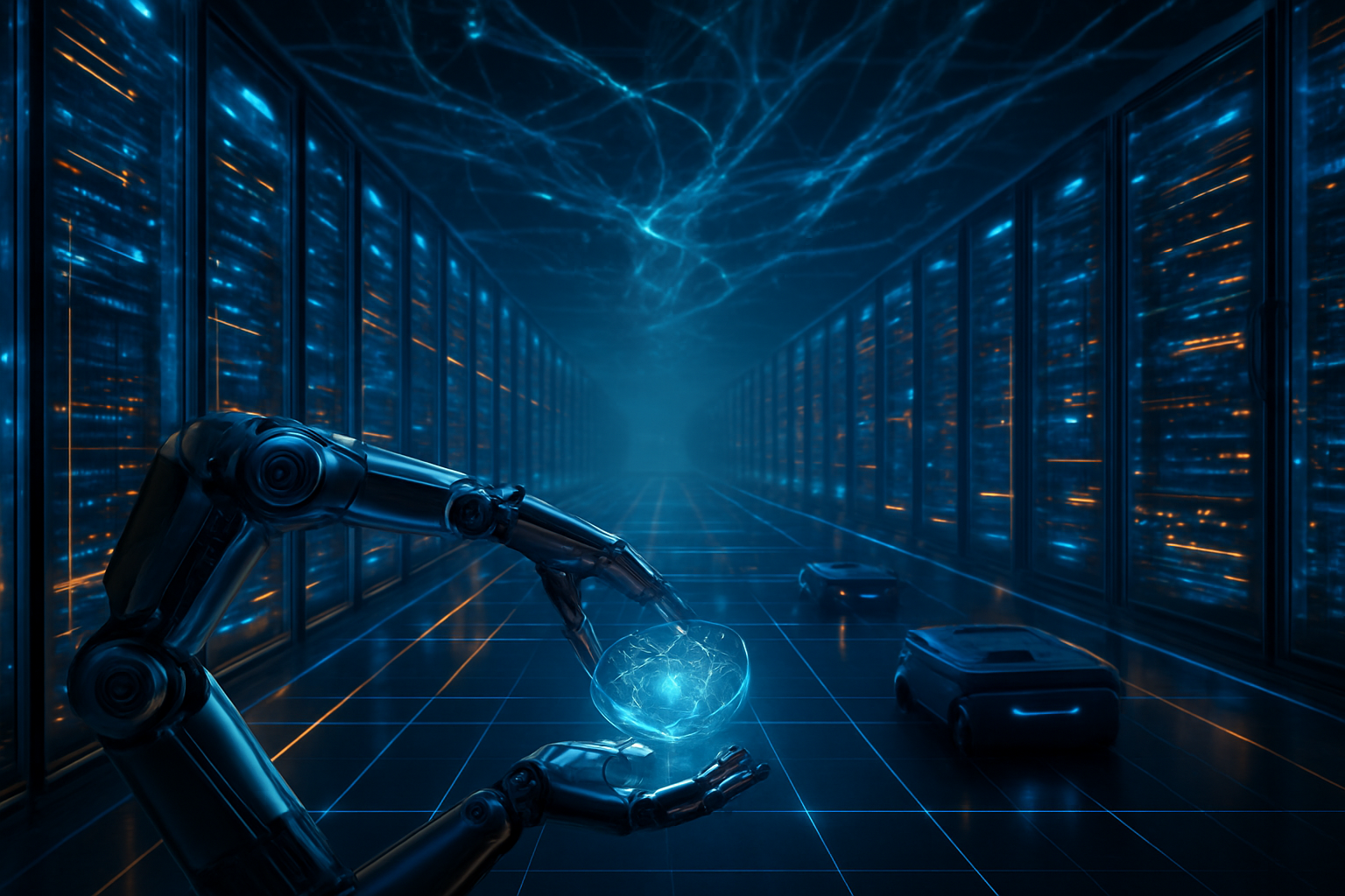
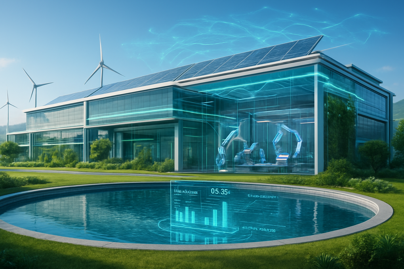
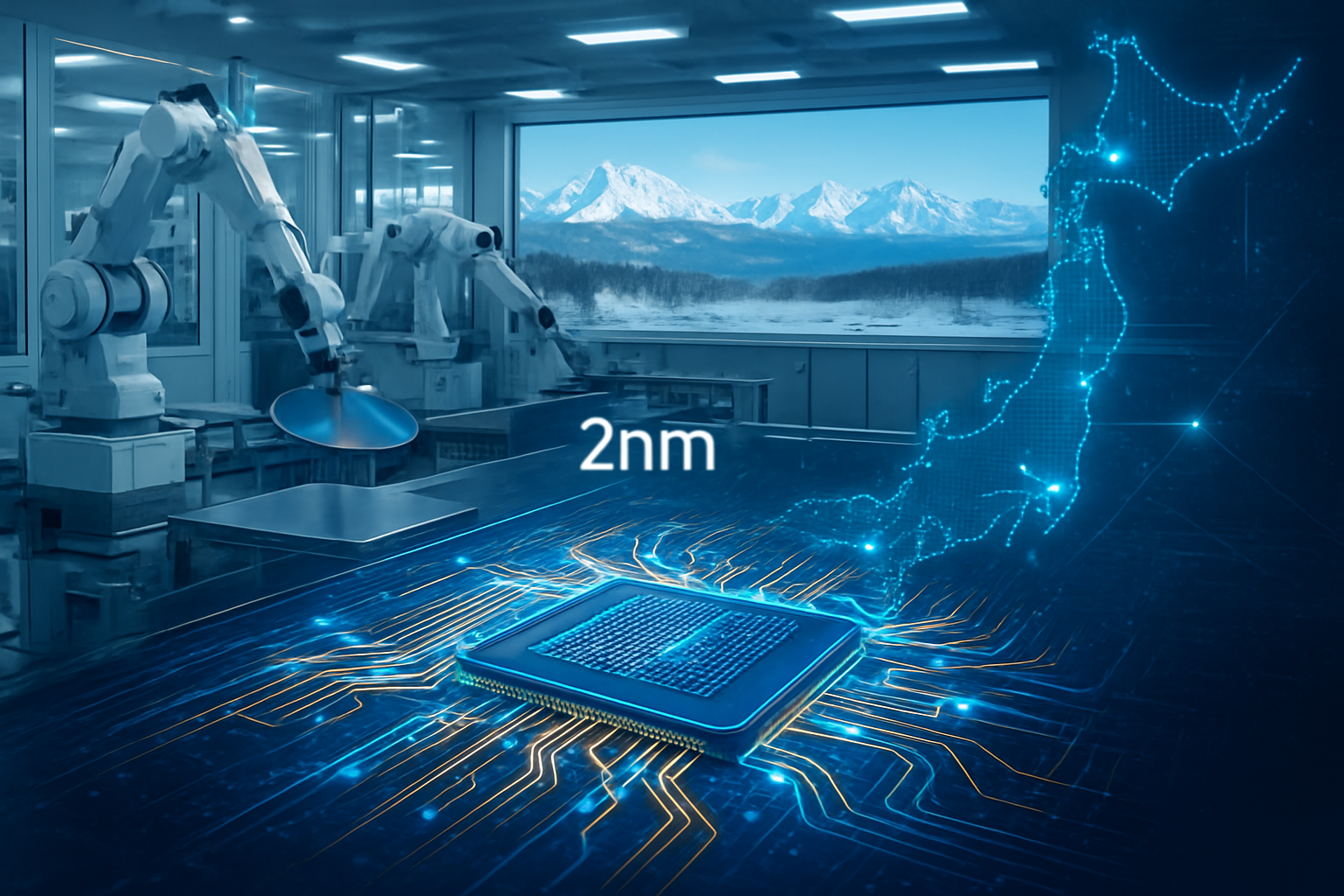
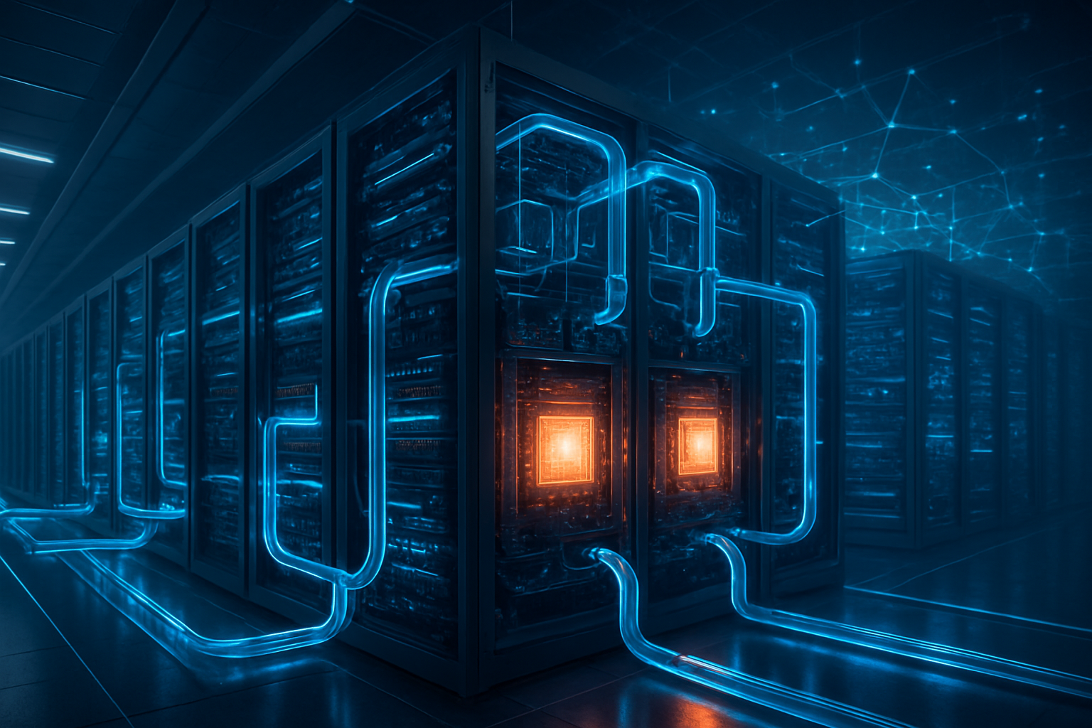
    At the heart of this funding round is the "Stargate" project, a joint infrastructure venture between OpenAI and its primary backers. As of February 2026, construction is already well underway at "Stargate One," a 4-million-square-foot flagship campus in Abilene, Texas. Unlike previous data centers, Stargate One is designed to operate on a scale previously thought impossible, utilizing the latest NVIDIA (NASDAQ: NVDA) Blackwell and "Rubin" GPU architectures alongside custom silicon developed in partnership with Amazon. The facility is pioneering the use of "behind-the-meter" nuclear power, aiming to bypass the strained public electrical grid by tapping directly into small modular reactors (SMRs).

    Technical specifications for the Stargate network are breathtaking. The roadmap aims to secure 10 gigawatts of power capacity by 2029, with international nodes already breaking ground in Abu Dhabi, Norway, and the United Kingdom. This differs from previous approaches by treating compute as a sovereign resource; rather than relying on distributed cloud instances, OpenAI is building a centralized, high-density compute monolith designed specifically for training "Orion," the rumored successor to its current frontier models. The industry consensus is that this level of dedicated hardware is necessary to overcome the "scaling laws" plateau, providing the raw FLOPS required for reasoning capabilities that mimic human intuition.

    Initial reactions from the AI research community have been a mixture of awe and caution. Dr. Elena Rossi, a senior researcher at the AI Ethics Lab, noted that "OpenAI is no longer just a research lab; they are becoming a global utility provider for intelligence." While some experts worry about the environmental impact of such massive energy consumption, others argue that the efficiency gains from custom-designed Stargate hardware could eventually lower the carbon footprint per inference compared to today’s fragmented infrastructure.

    A New Power Dynamic: Competitive Implications for the Tech Titan Hierarchy

    The participation of Amazon in this round is perhaps the most significant strategic shift of the year. Historically, Amazon had placed its primary bets on OpenAI’s rival, Anthropic. By contributing a reported $50 billion to this round—partly in the form of compute credits and custom "Trainium" chip integration—Amazon has effectively hedged its position in the AI landscape. This move places Amazon in a unique dual-partnership role, ensuring its AWS infrastructure remains the backbone for the world’s most dominant AI models while gaining a seat at the table of OpenAI's board as an observer.

    For other major players like Alphabet (NASDAQ: GOOGL) and Meta (NASDAQ: META), the $830 billion valuation raises the stakes for their own internal AI investments. The capital allows OpenAI to outbid any competitor for top-tier engineering talent and secure long-term supply chain priority for specialized chips. Startups, meanwhile, face an increasingly bifurcated market. While the "Big Three" (OpenAI, Anthropic, and Google) consolidate the foundation model space with massive capital moats, smaller labs are being pushed toward niche, vertical-specific AI applications where they can compete on efficiency rather than raw power.

    The strategic advantage for OpenAI also extends to its upcoming IPO. By securing $100 billion in private capital now, the company has removed the immediate pressure to go public in a volatile market, allowing it to complete its transition into a Public Benefit Corporation (PBC) without the quarterly scrutiny of public shareholders. This restructuring, finalized in late 2025, removed the profit caps that previously limited investor returns, clearing a path for a potential $1 trillion valuation once the company eventually lists on the Nasdaq.

    The $830 Billion Question: Wider Significance and Global Implications

    The massive valuation and the "Stargate" project represent more than just a corporate milestone; they signal the beginning of the "Sovereign AI" era. With sovereign wealth funds like Abu Dhabi’s MGX participating in the infrastructure build-out, AI is being treated with the same geopolitical importance as oil or semiconductor manufacturing. The move toward 10 gigawatts of power capacity also places OpenAI at the center of the global energy transition, forcing a rapid acceleration in nuclear and renewable energy policy to meet the insatiable demands of high-density compute.

    However, the $830 billion valuation has also drawn intense scrutiny from regulators and economists. Concerns regarding "AI hyper-concentration" are mounting in both Washington and Brussels, with some lawmakers arguing that the capital requirements for AGI are creating a natural monopoly that no new entrant could ever challenge. Comparisons are being drawn to the early 20th-century build-out of the electrical grid or the telecommunications boom of the 1990s, where the entities that controlled the physical infrastructure held immense power over the digital economy.

    Furthermore, the sheer size of the "Stargate" project has sparked a debate about the "intelligence-to-power" ratio. As OpenAI pushes the limits of physical scaling, the industry is watching closely to see if doubling the compute will continue to yield proportional improvements in model capability. If the scaling laws begin to show diminishing returns, the $100 billion investment could represent one of the most expensive experiments in human history.

    Looking Ahead: The Road to the $1 Trillion IPO

    In the near term, the focus remains on "steel in the ground." Over the next 12 to 18 months, OpenAI is expected to activate the first phase of the Texas Stargate facility, which will reportedly host the training run for its first truly multimodal, agentic system capable of autonomous software engineering and complex scientific discovery. These "Agentic Workflows" are predicted to be the primary revenue driver leading into the 2026 IPO, shifting ChatGPT from a chatbot into a comprehensive productivity operating system.

    The primary challenges ahead are logistical and regulatory. Securing the necessary permits for nuclear-powered data centers and navigating antitrust inquiries from the FTC and European Commission will be the main hurdles for OpenAI’s leadership team, led by CEO Sam Altman and CFO Sarah Friar. Market analysts predict that if OpenAI can demonstrate a clear path to $50 billion in annual recurring revenue (ARR) through its enterprise and infrastructure services, a 2026 IPO could see the company debut at a valuation exceeding $1.2 trillion, making it one of the most valuable entities on the planet.

    Summary: A Defining Chapter in AI History

    The $100 billion funding round and the $830 billion valuation mark the end of the "startup" era for OpenAI. By securing the capital necessary to build the world’s most advanced physical infrastructure, the company has effectively declared its intention to lead the transition to AGI. The involvement of tech giants like Amazon and SoftBank signals a consolidation of power, where the line between cloud providers, chip makers, and AI researchers is becoming increasingly blurred.

    As we watch the development of the Stargate network over the coming months, the key indicators of success will be the successful activation of new power sources and the deployment of models that can justify this historic level of investment. For now, OpenAI has set a new high-water mark for what it means to be a "tech company" in the age of artificial intelligence, turning the world’s eyes toward a future where intelligence is as ubiquitous and essential as electricity.


    This content is intended for informational purposes only and represents analysis of current AI developments.

    TokenRing AI delivers enterprise-grade solutions for multi-agent AI workflow orchestration, AI-powered development tools, and seamless remote collaboration platforms.
    For more information, visit https://www.tokenring.ai/.

  • Amazon’s $200 Billion AI Gambit: Andy Jassy Charges into the ‘Arms Race’ Despite Market Backlash

    Amazon’s $200 Billion AI Gambit: Andy Jassy Charges into the ‘Arms Race’ Despite Market Backlash

    In a move that has sent shockwaves through both Silicon Valley and Wall Street, Amazon.com Inc. (NASDAQ: AMZN) has officially confirmed a staggering $200 billion capital expenditure plan for the 2026 fiscal year. The announcement, delivered during the company’s Q4 earnings call on February 5, 2026, marks the single largest one-year investment by a private enterprise in history. Focused heavily on a "triple-threat" strategy of AI infrastructure, custom silicon, and advanced robotics, the plan signals CEO Andy Jassy’s absolute commitment to winning what he describes as a "generational arms race" against Alphabet Inc. (NASDAQ: GOOGL) and Microsoft Corp. (NASDAQ: MSFT).

    The immediate market reaction, however, was one of "sticker shock." Shares of Amazon plummeted 10% in after-hours trading and early morning sessions as investors grappled with the sheer scale of the spending. Despite AWS posting a robust 24% year-over-year revenue growth, the massive outlay has stoked fears regarding near-term margin compression and the timeline for a return on investment. Jassy remained undeterred during the call, framing the $200 billion figure not as a speculative bet, but as a necessary response to a "seminal inflection point" in the global economy.

    Silicon and Steel: The Technical Core of the $200 Billion Plan

    The lion’s share of the $200 billion investment is earmarked for AWS’s physical and digital foundation, with a significant pivot toward custom hardware. Central to this strategy is the general availability of Trainium 3, Amazon’s latest AI-specialized chip. Fabricated on a cutting-edge 3nm process by Taiwan Semiconductor Manufacturing Company (NYSE: TSM), Trainium 3 reportedly offers a 4.4x increase in compute performance and 4x better energy efficiency compared to its predecessor. By deploying these chips in "UltraServer" clusters capable of scaling up to one million interconnected units, Amazon aims to provide the massive compute required to train the next generation of trillion-parameter models, such as those being developed by its lead partner, Anthropic.

    In addition to silicon, Amazon is aggressively scaling its "Physical AI" capabilities within its logistics network. The company revealed the rollout of Vulcan, a new tactile robotic arm equipped with advanced force-feedback sensors. Unlike previous iterations, Vulcan possesses a "sense of touch," allowing it to handle fragile items and pick-and-pack approximately 75% of Amazon's diverse inventory—a threshold that has long been the "holy grail" of warehouse automation. This is supported by DeepFleet AI, a generative AI orchestration layer that manages the movement of over 1.2 million autonomous robots, including the fully mobile Proteus units, across hundreds of fulfillment centers globally.

    The technical shift represents a departure from the industry’s heavy reliance on Nvidia Corp. (NASDAQ: NVDA). While Amazon remains a major purchaser of Blackwell and subsequent Nvidia architectures, the $200 billion plan places a heavy emphasis on vertical integration. By designing the chips, the servers, and the robotic controllers in-house, Amazon claims it can reduce the total cost of ownership for AI workloads by up to 40%, offering a price-to-performance ratio that third-party hardware providers may struggle to match as the "arms race" intensifies.

    The Cloud Hierarchy: Competitive Implications for the Big Three

    Amazon's aggressive spending redefines the competitive landscape for cloud dominance. For years, Microsoft and Google have leveraged their early leads in generative AI to challenge AWS's market share. However, Jassy’s 2026 plan is an attempt to use Amazon’s massive scale to outbuild the competition. While Microsoft has leaned heavily on its partnership with OpenAI and Google has integrated Gemini across its ecosystem, Amazon is positioning itself as the "foundational layer" for all AI development. By offering the most cost-effective training environment via Trainium 3, Amazon hopes to lure startups and enterprises away from Azure and Google Cloud.

    The $200 billion commitment also serves as a strategic defensive move. As Google and Microsoft continue to report multi-billion dollar capex increases, Amazon’s decision to double down ensures it will not be "out-provisioned" in the race for data center capacity. This has significant implications for AI labs; with Anthropic already scaling its workloads to nearly one million Trainium chips, Amazon is effectively securing its position as the primary host for the world’s most advanced models. This "infrastructure-first" approach may force competitors to either match the spending—further straining their own margins—or risk losing high-value enterprise clients who require guaranteed compute availability.

    Furthermore, the integration of robotics gives Amazon a unique edge that its cloud-only competitors lack. While Google and Microsoft focus on digital intelligence, Amazon is applying AI to the physical world at a scale no other company can match. This dual-track strategy—leading in both virtual cloud services and physical logistics automation—creates a "flywheel" effect where gains in AI efficiency directly lower the cost of retail operations, which in turn provides more capital to reinvest in AI infrastructure.

    A New Milestone in the Global AI Landscape

    The scale of Amazon's 2026 plan reflects a broader shift in the AI landscape from experimentation to industrial-scale deployment. We are moving past the era of "chatbots" and entering an age where AI is a fundamental utility, akin to electricity or the internet itself. Amazon’s $200 billion bet is the largest signal to date that the tech industry views AI as the definitive backbone of future global commerce. Comparing this to previous milestones, such as the initial build-out of the 4G/5G networks or the early internet backbone, the current AI infrastructure boom is significantly more capital-intensive and concentrated among a few "hyper-scalers."

    However, this massive expansion brings significant concerns, most notably regarding energy consumption and environmental impact. Building out the data center capacity to support $200 billion in hardware requires an immense amount of power. Amazon has stated it is investing heavily in small modular reactors (SMRs) and other carbon-free energy sources, but the sheer speed of the build-out has raised questions about the strain on local power grids and the company’s ability to meet its "Net Zero" commitments by 2040.

    The 10% stock drop also highlights a growing tension between Silicon Valley’s long-term vision and Wall Street’s demand for quarterly discipline. There is a palpable fear that the industry is entering a "capex bubble" where the cost of building AI far outstrips the immediate revenue it generates. Jassy’s insistence that this is a "demand-led" investment will be put to the test throughout 2026. If AWS cannot maintain its 24%+ growth rate, the pressure from institutional investors to pull back on spending will become deafening.

    The Horizon: What Comes Next for the AI Titan?

    Looking ahead, the next 12 to 18 months will be a proving ground for Amazon’s "Physical AI" vision. The successful integration of the Vulcan tactile arms across the fulfillment network is expected to be a major catalyst for margin expansion in the retail sector, potentially offsetting the high costs of the infrastructure build-out. Experts predict that if Amazon can successfully automate 75% of its picking and stowing operations by the end of 2026, it could see a permanent 15-20% reduction in fulfillment costs, a move that would fundamentally alter the economics of e-commerce.

    In the near term, all eyes will be on the performance of Trainium 3 in real-world benchmarks. If Amazon’s custom silicon can indeed outperform Nvidia’s offerings on a price-per-watt basis, we may see a significant shift in how AI models are trained. We also expect to see the "DeepFleet" orchestration model being offered as a standalone service for other logistics and manufacturing companies, potentially opening a new multibillion-dollar revenue stream for AWS in the industrial AI sector.

    Challenges remain, particularly in the realm of regulatory scrutiny. As Amazon becomes the dominant provider of both the "brains" (AI chips) and the "brawn" (logistics robotics) of the modern economy, antitrust regulators in both the U.S. and E.U. are likely to take a closer look at its vertical integration. Balancing this rapid expansion with global regulatory compliance will be one of Jassy’s most difficult tasks in the coming years.

    Conclusion: A Generational Bet on the Future of Intelligence

    Amazon’s $200 billion capital expenditure plan for 2026 is a watershed moment in the history of technology. It is a bold, high-stakes declaration that the company intends to own the foundational infrastructure of the AI era, from the silicon wafers in the data center to the robotic fingers in the warehouse. While the 10% drop in stock price reflects immediate investor anxiety, it does little to dampen the long-term strategic trajectory set by Andy Jassy.

    The significance of this development cannot be overstated; it marks the transition of AI from a software-driven innovation to a hardware-and-infrastructure-dominated industry. As the "arms race" with Google and Microsoft reaches its zenith, Amazon is betting that the company with the most efficient, most integrated, and most massive physical footprint will ultimately win. In the coming months, the performance of AWS and the successful rollout of the Vulcan robotics system will be the key metrics to watch. For now, Amazon has made its move—and it is the largest the world has ever seen.


    This content is intended for informational purposes only and represents analysis of current AI developments.

    TokenRing AI delivers enterprise-grade solutions for multi-agent AI workflow orchestration, AI-powered development tools, and seamless remote collaboration platforms.
    For more information, visit https://www.tokenring.ai/.

  • The Great Decoupling: How RISC-V Achieved Architecture Sovereignty in 2026

    The Great Decoupling: How RISC-V Achieved Architecture Sovereignty in 2026

    As of February 2026, the global semiconductor landscape has undergone a tectonic shift, marking the end of the long-standing x86 and ARM duopoly. RISC-V, the open-standard Instruction Set Architecture (ISA), has matured from a promising academic project into a dominant industrial powerhouse. This evolution is most visible in the automotive and Internet of Things (IoT) sectors, where the architecture now commands a staggering 25% and 55% of new design wins respectively. By offering a royalty-free, highly customizable alternative, RISC-V has become the cornerstone of the "Software-Defined Everything" era, enabling a new level of hardware-software co-design that was previously impossible under restrictive proprietary licenses.

    The significance of this milestone cannot be overstated. For decades, chip designers were forced to choose between the high-performance but power-hungry x86 architecture or the efficient but strictly controlled ARM ecosystem. Today, RISC-V provides a third pillar that balances performance with unprecedented flexibility. This "architecture sovereignty" allows tech giants and startups alike to bake their own proprietary AI accelerators and safety features directly into the processor core. As the industry moves toward 2027, the "ARM Tax"—the multi-million dollar licensing fees and per-chip royalties—has shifted from a standard business expense to a competitive liability, driving a massive migration toward the open-source frontier.

    Technical Maturity: From Embedded Controllers to High-Performance AI

    The technical breakthrough that defined 2025 and 2026 was the finalization and widespread implementation of the RVA23 profile. Previously, RISC-V faced criticism for "fragmentation," where different chip makers implemented features in incompatible ways. The RVA23 standard unified the ecosystem, providing a stable baseline for operating systems like Android and enterprise Linux distributions. In April 2026, the release of Ubuntu 26.04 LTS became a landmark event, offering the first long-term supported enterprise OS with native, high-performance optimization for RISC-V, effectively putting it on equal footing with x86 for server and edge applications.

    A key technical differentiator in 2026 is the RISC-V Vector (RVV) 1.0 extension. Unlike ARM (Nasdaq: ARM) or Intel (Nasdaq: INTC) architectures, which often require separate, specialized AI chips, RISC-V’s vector extensions allow for massive parallel processing of AI workloads directly within the CPU. Companies like Tenstorrent and SiFive have released "Ascalon-class" cores that rival the performance of ARM’s Neoverse V3. These chips use 512-bit vector widths to handle complex sensor fusion and machine learning telemetry in real-time, which has proven critical for the low-latency requirements of autonomous systems.

    Furthermore, the rise of "Shift-Left" development methodologies has been accelerated by RISC-V’s open nature. Automakers are now using "Digital Twins" of RISC-V hardware—fully functional software models of the chip—to begin writing and testing vehicle code years before a physical chip is even manufactured. This has reduced the development cycle for new vehicle platforms from the traditional five years down to just three. Because the ISA is open, developers can inspect every instruction, ensuring that safety-critical "Zero Trust" security protocols are hard-coded into the silicon, a level of transparency that proprietary architectures cannot match.

    The software ecosystem has finally caught up to the hardware. In late 2025, Google (Nasdaq: GOOGL) designated RISC-V as a "Tier 1" architecture for Android, finalizing the Native Development Kit (NDK) and Application Binary Interface (ABI). This move has paved the way for the first wave of commercial RISC-V smartphones appearing in early 2026. While these devices currently target the mid-range and budget markets in Asia, the technical foundation is now in place for RISC-V to challenge ARM’s 95% dominance of the mobile processor market by the end of the decade.

    The Economic Earthquake: Challenging the ARM and x86 Giants

    The maturation of RISC-V has sent shockwaves through the boardrooms of established chip giants. Qualcomm (Nasdaq: QCOM), once one of ARM’s largest customers, has aggressively pivoted toward RISC-V following high-profile licensing disputes. By acquiring Ventana Micro Systems in 2025, Qualcomm has begun integrating its own high-performance RISC-V cores into its Snapdragon automotive and IoT platforms. This strategic move allows Qualcomm to bypass ARM’s restrictive licensing terms and potentially save billions in royalty payments over the next decade, while gaining the freedom to innovate at the instruction level.

    In the automotive sector, the Quintauris joint venture—a powerhouse consortium including Bosch, Infineon (OTC: IFNNY), Nordic Semiconductor, NXP (Nasdaq: NXPI), and Qualcomm—has successfully established a standardized RISC-V platform for Software-Defined Vehicles (SDVs). By early 2026, this venture has turned RISC-V into the industry standard for zonal controllers, the "brains" that manage everything from power steering to infotainment. This collective approach has effectively neutralized ARM’s historical advantage in the automotive space, as manufacturers now prefer a communal, open-source architecture that no single company can gatekeep or monopolize.

    The impact on the IoT market has been even more dramatic. With over 55% of new IoT designs now utilizing RISC-V, the architecture has become the default choice for connected devices. The royalty-free model has reduced bill-of-materials (BOM) costs by as much as 50% for high-volume sensors and smart home devices. This cost advantage has allowed companies to reinvest savings into more robust on-device AI and security features. For startups, the low barrier to entry provided by RISC-V has sparked a renaissance in "bespoke silicon," where small teams can design custom chips for niche industrial applications without the $10 million+ upfront licensing costs associated with proprietary ISAs.

    Legacy players are reacting with varying degrees of urgency. While Intel has embraced RISC-V through its foundry services (IFS), offering to manufacture RISC-V chips for others, it faces a long-term threat to its x86 dominance in the data center. Meta (Nasdaq: META) and NVIDIA (Nasdaq: NVDA) have already integrated millions of RISC-V cores into their internal infrastructure—Meta for its MTIA AI inference accelerators and NVIDIA for managing telemetry and secure boot across its entire GPU lineup. For these giants, RISC-V isn't just a cost-saving measure; it’s a strategic tool for vertical integration, allowing them to control the entire stack from the silicon to the cloud.

    A New Era of Open-Source Infrastructure and Global Resilience

    The rise of RISC-V in 2026 represents a broader trend toward technological de-globalization and national self-reliance. As trade tensions continue to influence the tech sector, RISC-V has emerged as a "neutral" architecture. Because no single nation or company owns the ISA, it serves as a common language for global innovation that is immune to specific export bans or entity-list restrictions. This has made RISC-V particularly attractive in the European Union and Asia, where governments are subsidizing open-source hardware projects to ensure their domestic industries are not overly dependent on US- or UK-based IP.

    This shift mirrors the "Linux moment" for hardware. Just as Linux broke the monopoly of proprietary operating systems in the 1990s and 2000s, RISC-V is doing the same for the processor world. The architecture has fostered a massive, global community of contributors, ensuring that security vulnerabilities are patched faster and optimizations are shared more broadly than in closed ecosystems. The 2026 landscape shows that "Security through Transparency" has won over "Security through Obscurity," with many government agencies now mandating RISC-V for critical infrastructure to ensure there are no hidden backdoors in the silicon.

    However, this transition has not been without its challenges. The industry has had to grapple with the "Wild West" period of RISC-V development, where early adopters struggled with a lack of standardized tools and middleware. The successful stabilization of the ecosystem in 2026 is largely credited to the RISC-V International organization, which managed to herd the competing interests of hundreds of member companies toward a common goal. This level of industry cooperation is unprecedented and serves as a model for how other complex technologies, such as quantum computing and advanced robotics, might be governed in the future.

    Comparisons to previous AI milestones are frequent. Analysts often liken the maturity of RISC-V to the launch of ChatGPT—a moment where a technology that had been "bubbling under the surface" for years suddenly achieved the performance and accessibility needed to change the world overnight. While ChatGPT revolutionized how we interact with data, RISC-V is revolutionizing the physical substrate upon which that data is processed. It is the silent engine driving the AI revolution at the edge, making sophisticated intelligence affordable, customizable, and ubiquitous.

    The Horizon: AI-Native Silicon and the Path to the Data Center

    Looking ahead to 2027 and beyond, the focus of the RISC-V community is shifting toward the high-performance computing (HPC) and server markets. While RISC-V has conquered IoT and made significant inroads into automotive, the data center remains the "final frontier" currently dominated by x86 and ARM. Experts predict that the next two years will see the rise of "AI-Native" servers, where RISC-V’s modularity allows for the seamless integration of hundreds of specialized neural cores on a single die. This could potentially disrupt the server market by offering significantly higher performance-per-watt for the specific math required by Large Language Models (LLMs).

    We are also likely to see the emergence of the first true "Open-Source Consumer Ecosystem." With Android support finalized, the dream of a fully open-source laptop and smartphone—from the hardware instructions to the kernel to the user interface—is becoming a reality. This will likely appeal to a growing market of privacy-conscious consumers and enterprise users who require absolute control over their hardware. The challenge will be in hardware-software optimization; while RISC-V is capable, it will take time to match the decades of "fine-tuning" that Intel and Apple (Nasdaq: AAPL) have applied to their proprietary platforms.

    Predictions for 2028 suggest that RISC-V will reach 15% of the total CPU market share, a meteoric rise considering its near-zero presence a decade prior. To reach this goal, the ecosystem must address the remaining gaps in high-end developer tools and ensure a steady pipeline of talent. Universities worldwide have already shifted their computer architecture curricula to center on RISC-V, ensuring that the next generation of engineers is "native" to the open-source model. As the "great decoupling" from proprietary architectures continues, the momentum behind RISC-V appears not just sustainable, but inevitable.

    Summary of a New Computing Paradigm

    The state of RISC-V in early 2026 is one of undeniable maturity and massive momentum. What began as a research project at UC Berkeley has fundamentally reordered the $600 billion semiconductor industry. By dominating the IoT sector and becoming the standard for the next generation of Software-Defined Vehicles, RISC-V has proven that an open-source model can outpace and out-innovate even the most entrenched proprietary giants. The royalty-free nature of the ISA has democratized silicon design, sparking a wave of innovation that is bringing AI and advanced connectivity to every corner of the global economy.

    As we move through 2026, the industry should watch for the first commercial RISC-V mobile devices and the continued expansion of RISC-V into the data center. The "Architecture Wars" are far from over, but the battlefield has changed. No longer is the question whether RISC-V is viable; the question is how quickly the remaining proprietary strongholds will adapt to a world where the foundations of computing are free, open, and available to all. The "Great Decoupling" is here, and it is powered by RISC-V.


    This content is intended for informational purposes only and represents analysis of current AI and semiconductor developments as of February 2026.

    TokenRing AI delivers enterprise-grade solutions for multi-agent AI workflow orchestration, AI-powered development tools, and seamless remote collaboration platforms.
    For more information, visit https://www.tokenring.ai/.

  • The Silicon Revolution Turns Green: Inside the Rise of the Net-Zero ‘Mega-Fab’ in 2026

    The Silicon Revolution Turns Green: Inside the Rise of the Net-Zero ‘Mega-Fab’ in 2026

    As of February 6, 2026, the global semiconductor industry has reached a historic inflection point where environmental sustainability is no longer a peripheral corporate goal but a core requirement for high-end chip production. Driven by aggressive climate targets and a fundamental shift in regulatory landscapes across the United States and Europe, the race to build the world's first truly "Green Fabs" has moved from the boardroom to the construction site. For the first time, major chipmakers are successfully de-coupling the exponential growth of artificial intelligence and high-performance computing from their historic environmental footprints.

    The immediate significance of this shift is profound: the "Big Three"—Intel (NASDAQ: INTC), TSMC (NYSE: TSM), and Samsung (KRX: 005930)—are now competing as much on their carbon-per-wafer metrics as they are on nanometer scales. In early 2026, the launch of Intel’s Fab 52 in Arizona and the commissioning of TSMC’s Industrial Water Reclamation Plant in Phoenix have set a new standard for "water-positive" manufacturing. These facilities are proving that even in arid, drought-prone regions, advanced chipmaking can exist without depleting local resources, marking a critical victory for the industry’s long-term viability.

    Engineering the Circular Fab: Beyond Net-Zero

    The technical evolution of the 2026 "Green Fab" is defined by a transition toward near-total circularity, specifically in the management of water and chemicals. Modern facilities are now deploying Industrial Water Reclamation Plants (IWRP) that utilize Electrodialysis Reversal (EDR) and Forward Osmosis (FO) to achieve water recycling rates exceeding 90%. Unlike previous generations of "reclamation," which only treated gray water for cooling towers, these 2026 systems can remove dissolved metals like Copper and Manganese down to parts-per-billion levels, allowing the water to be recycled back into the Ultra-Pure Water (UPW) stream required for sensitive lithography steps.

    A major breakthrough in early 2026 is the successful transition to PFAS-free chemicals in high-volume manufacturing. While "forever chemicals" were long considered essential for the precision required in EUV (Extreme Ultraviolet) lithography, companies like Fujifilm (OTC: FUJIY) and Central Glass have finally brought commercially viable PFAS-free photoresists to market. These new formulations eliminate per- and polyfluoroalkyl substances while maintaining the high resolution necessary for 2nm nodes. While the industry is still grappling with PFAS-free alternatives for dry etching, new Point-of-Use (POU) Abatement Systems installed in 2026-era fabs can now capture and destroy 99.9% of these emissions before they leave the facility.

    To manage the immense power demands of these "Mega-Fabs," 2026 marks the widespread adoption of AI-driven Digital Twins. Utilizing platforms from Siemens (ETR: SIE) and NVIDIA (NASDAQ: NVDA), plant managers now use real-time 3D replicas of their facilities to simulate "What-If" scenarios. These AI models predict HVAC loads based on external weather patterns and optimize chiller plant efficiency, reducing total energy overhead by up to 20%. This level of optimization allows fabs to function as "prosumers" on the energy grid, using on-site solar arrays and massive battery storage systems to balance the load during peak demand without sacrificing 100% renewable uptime.

    The Business of Green Silicon: Winners and the "Green Premium"

    The move toward sustainable manufacturing has birthed a new economic reality: the "Green Premium." In early 2026, chips produced in certified carbon-neutral or water-positive facilities carry an estimated price premium of 5% to 15%. However, this cost is being eagerly absorbed by tech giants like Apple (NASDAQ: AAPL) and Microsoft (NASDAQ: MSFT). Apple has reportedly secured nearly 50% of TSMC's 2nm "Green" capacity for 2026, using its high-margin "Pro" and "Ultra" device tiers to insulate consumers from the increased manufacturing costs.

    Microsoft, meanwhile, has institutionalized a carbon-neutral supply chain through its Internal Carbon Fee Model. By charging its internal business units (such as Azure and Xbox) for their carbon footprints, Microsoft has created a massive fund to subsidize Green Power Purchase Agreements (PPAs) and invest in carbon removal credits. This strategic positioning gives these tech giants a competitive edge in an era where institutional investors and ESG-conscious consumers demand transparency. Startups and mid-tier chip companies, however, face a tougher challenge, as they lack the capital to invest in the $300 million on-site reclamation plants that define the modern green facility.

    The strategic map of the industry is also shifting due to these sustainability demands. While Intel (NASDAQ: INTC) has pushed ahead with its "Silicon Heartland" project in Ohio—featuring a state-funded water reclamation plant—it has officially paused its Magdeburg project in Germany as of February 2026 due to financial restructuring and cooling European demand. This move highlights a growing divergence: the "Green Revolution" is currently most active where government subsidies, like those from the US CHIPS Act, are explicitly tied to environmental milestones.

    Regulating the Future: From CSR to Compliance

    In 2026, the transition to green fabs has moved beyond voluntary Corporate Social Responsibility (CSR) into the realm of strict regulatory compliance. The US EPA’s TSCA Section 8 reporting deadline passed in January 2026, forcing semiconductor firms to submit a decade's worth of data on PFAS usage. This transparency is now driving a "compliance enforcement" phase where investors can see exactly which companies are lagging in their chemical transitions. In Europe, while the ECHA (European Chemicals Agency) is considering a 13.5-year "essential use" exemption for certain semiconductor processes, the pressure to innovate away from PFAS remains immense.

    This regulatory environment is fundamentally different from the 2020-2022 era. The "Green Fab" is now a geopolitical asset. Nations that can provide both the massive power grids required for 2nm production and the renewable energy to back it up are becoming the preferred hubs for the next generation of AI silicon. This has led to a "race to the top" in environmental standards, as countries compete to attract investment by offering "Green Microgrids" and integrated water management infrastructure as part of their industrial incentives.

    However, concerns remain regarding the "Scope 3" emissions of the semiconductor industry—the carbon footprint of the entire supply chain, from raw material mining to end-of-life disposal. While the fabs themselves are becoming cleaner, the extraction of rare earth metals remains an environmental bottleneck. To address this, 2026 has seen the rise of "closed-loop agreements," where companies like Apple return end-of-life hardware to recyclers who recover Cobalt and Neodymium, which are then fed back into the manufacturing pipeline, effectively "paying" for new chips with recycled materials.

    Looking Ahead: The Autonomous, Prosumer Fab

    The next phase of green manufacturing, expected between 2027 and 2030, will likely focus on the complete elimination of fluorinated gases in etching—a feat that has remained the "final frontier" of green chemistry. Researchers are currently pilot-testing "Fluorine, Argon, Nitrogen" (FAN) gas mixtures as non-PFAS alternatives for cleaning and etching, with early results suggesting a potential rollout in late 2027. If successful, this would allow fabs to finally claim a PFAS-free status across the entire manufacturing flow.

    Furthermore, the role of the fab in the local community is evolving. Experts predict that by 2028, new fabs will act as central nodes in regional "circular economies," sharing treated wastewater with local agriculture and providing excess heat from cleanrooms to warm local municipal buildings. This "Community-Integrated Fab" model would move the industry from being a resource drain to a resource provider, a shift that will be necessary to gain public approval for the next wave of "Giga-Fabs" planned for the end of the decade.

    A New Era for Silicon

    The emergence of sustainable "Green" fabs in 2026 represents a landmark achievement in the history of the semiconductor industry. What was once seen as an irreconcilable conflict between the massive resource demands of advanced computing and the need for environmental preservation is being resolved through technical ingenuity and strategic investment. The "Big Three" have proven that 90% water recycling and 100% renewable energy are not just aspirational goals, but operational realities of the modern 2nm and 3nm nodes.

    As we look toward the remainder of 2026, the industry’s progress will be measured by its ability to scale these green technologies beyond the flagship "Mega-Fabs" and into the broader global supply chain. The "Silicon Revolution" has officially turned green, and the chips powering the AI era are finally being built with the planet’s future in mind.


    This content is intended for informational purposes only and represents analysis of current AI developments.

    TokenRing AI delivers enterprise-grade solutions for multi-agent AI workflow orchestration, AI-powered development tools, and seamless remote collaboration platforms.
    For more information, visit https://www.tokenring.ai/.

  • The New Moore’s Law: How Chiplets and CoWoS are Redefining the Scaling Paradigm in the AI Era

    The New Moore’s Law: How Chiplets and CoWoS are Redefining the Scaling Paradigm in the AI Era

    The semiconductor industry has reached a historic inflection point. For five decades, the industry followed the traditional Moore’s Law, doubling transistor density by physically shrinking the components on a single piece of silicon. However, as of February 2026, that "geometrical scaling" has hit a physical and economic wall. In its place, a "New Moore’s Law"—more accurately described as System-level Moore’s Law—has emerged, shifting the focus from the individual chip to the entire package. This evolution is driven by the insatiable compute demands of generative AI, where performance is no longer defined by how many transistors can fit on a die, but by how many dies can be seamlessly stitched together in 3D space.

    The primary engines of this revolution are Chip-on-Wafer-on-Substrate (CoWoS) and vertical 3D stacking technologies. By abandoning the "monolithic" approach—where a processor is carved from a single piece of silicon—industry leaders are now building massive, multi-die systems that bypass the traditional limits of physics. This shift represents the most significant architectural change in computing history since the invention of the integrated circuit, effectively decoupling performance gains from the slow and increasingly expensive progress of lithography nodes.

    The Death of the Monolithic Die and the Rise of CoWoS-L

    The technical heart of this shift lies in overcoming the "reticle limit." For years, the maximum size of a single chip was restricted to approximately 858mm²—the physical size of the mask used in lithography. To build the massive processors required for 2026-era AI, such as the NVIDIA (NASDAQ: NVDA) Rubin R100, engineers have turned to Advanced Packaging. TSMC (NYSE: TSM) has pioneered CoWoS-L (Local Silicon Interconnect), which uses tiny silicon bridges to "stitch" multiple logic dies together on an organic substrate. This allows a single package to effectively behave as one massive processor, far exceeding the physical size limits of traditional manufacturing.

    Beyond mere size, the industry has moved into the realm of true 3D integration with System on Integrated Chips (SoIC). Unlike 2.5D packaging, where chips sit side-by-side, SoIC allows for "bumpless" hybrid bonding, stacking logic directly on top of logic or memory. This reduces the distance data must travel from millimeters to micrometers, slashing power consumption and nearly eliminating the latency that previously throttled AI performance. Initial reactions from the research community have been transformative; experts note that the interconnect density provided by SoIC is now a more critical metric for AI training speeds than the raw clock speed of the transistors themselves.

    Strategic Realignment: The System Foundry Model

    This transition has fundamentally altered the competitive landscape for tech giants and foundries. TSMC has maintained its dominance by aggressively expanding its advanced packaging capacity to over 140,000 wafers per month in early 2026. This "System Foundry" approach allows them to offer a full-stack solution: 2nm logic, 3D stacking, and CoWoS-L packaging. Meanwhile, Intel (NASDAQ: INTC) has pivoted its strategy to position its Advanced System Assembly and Test (ASAT) business as a standalone service. By offering Foveros Direct 3D and EMIB packaging to external customers, Intel is attempting to capture the growing market for custom AI ASICs from cloud providers like Amazon and Google.

    Advanced Micro Devices (NASDAQ: AMD) has also leveraged these developments to close the gap with market leaders. The newly released Instinct MI400 series utilizes SoIC-X technology to stack HBM4 memory directly onto the GPU logic, achieving a staggering 20 TB/s of memory bandwidth. This strategic move highlights the "Memory Wall" as the primary bottleneck in LLM training; by using vertical integration, AMD can provide memory capacities that were physically impossible under old monolithic designs. For startups and smaller AI labs, the emergence of chiplet "standardization" means they can now design custom accelerators using off-the-shelf high-performance chiplets, lowering the barrier to entry for specialized AI hardware.

    Solving the "Warpage Wall" and the Memory Bottleneck

    The wider significance of the "New Moore's Law" extends beyond performance; it is a response to the "Warpage Wall." As packages grow larger than 100mm per side to accommodate dozens of chiplets, traditional organic substrates tend to warp under the intense heat generated by 1,000-watt AI GPUs. This has led to the first commercial rollout of glass substrates in early 2026, led by Intel and Samsung (KOSPI: 005930). Glass provides superior thermal stability and flatness, enabling the ultra-fine interconnects required for next-generation 3D stacking.

    Furthermore, this era marks the beginning of the "System Technology Co-Optimization" (STCO) phase. Previously, chip design and packaging were separate steps; now, they are unified. This fits into the broader AI landscape by addressing the catastrophic power consumption of modern data centers. By integrating Silicon Photonics and Co-Packaged Optics (CPO) directly into the package, companies can now convert electrical signals to light within the processor itself. This bypasses the energy-intensive process of pushing electrons through copper cables, a milestone that compares in significance to the transition from vacuum tubes to transistors.

    The Road to the Trillion-Transistor Package

    Looking ahead, the industry is aligned on a singular goal: the trillion-transistor package by 2030. In the near term, we expect to see the "Base Die" revolution, where the bottom layer of a 3D stack handles all power delivery and routing, leaving the top layers dedicated purely to computation. This will likely lead to "liquid-to-chip" cooling becoming a standard requirement for high-end AI clusters, as the heat density of 3D-stacked chips begins to exceed the limits of traditional air and even current water-cooling methods.

    However, challenges remain. The complexity of testing 3D-stacked chips is immense—if one "chiplet" in a stack of ten is faulty, the entire expensive package may be lost. Experts predict that "Self-Healing Silicon," which can reroute circuits around manufacturing defects in real-time, will be the next major area of research. Additionally, the geopolitical concentration of advanced packaging capacity in Taiwan remains a point of concern for global supply chain resilience, prompting a frantic race to build similar facilities in the United States and Europe.

    A New Architecture for a New Era

    The evolution of chiplets and CoWoS represents more than just a clever engineering workaround; it is a fundamental shift in how humanity builds thinking machines. The "New Moore’s Law" acknowledges that while we can no longer make transistors significantly smaller, we can make the systems they inhabit significantly more complex and efficient. The transition from 2D to 3D, and from copper to light, ensures that the AI revolution will not be throttled by the physical limits of a single silicon wafer.

    As we move through 2026, the primary metric of progress will be "transistors per package." With the arrival of glass substrates, HBM4, and 3D SoIC, the roadmap for AI hardware has been extended by another decade. The coming months will be defined by the "Packaging Wars," as foundries and chip designers race to secure the capacity needed to build the world’s most powerful systems. The monolithic era is over; the era of the integrated system has begun.


    This content is intended for informational purposes only and represents analysis of current AI developments.

    TokenRing AI delivers enterprise-grade solutions for multi-agent AI workflow orchestration, AI-powered development tools, and seamless remote collaboration platforms.
    For more information, visit https://www.tokenring.ai/.

  • India’s Silicon Sovereignty: The 2026 Emergence of a Global Semiconductor Powerhouse

    India’s Silicon Sovereignty: The 2026 Emergence of a Global Semiconductor Powerhouse

    As of February 6, 2026, the global technology landscape has undergone a tectonic shift. India, once viewed as merely a software services giant, has successfully pivoted to become a cornerstone of the world’s hardware supply chain. The "Made in India" chip is no longer a strategic ambition but a commercial reality, with major manufacturing facilities officially coming online this month. This transformation is anchored by the aggressive $18 billion India Semiconductor Mission (ISM), which has successfully leveraged government incentives to attract over $90 billion in cumulative private investment.

    The immediate significance of this development cannot be overstated. By establishing a robust presence in both front-end wafer fabrication and back-end assembly, India has provided the global tech industry with a much-needed "China Plus One" alternative. With the recent commencement of full-scale commercial production at Micron Technology, Inc. (NASDAQ: MU) in Sanand, Gujarat, India has entered the elite league of nations capable of high-volume semiconductor manufacturing, fundamentally altering the risk profile of the global electronics trade.

    From Groundbreaking to Grid-Scale Production: The Technical Milestone

    The technical cornerstone of India’s 2026 semiconductor success is the transition from pilot testing to mass-market output. Micron Technology’s $2.75 billion facility in Sanand is now operating at peak capacity, churning out high-density DRAM and NAND flash memory chips. These components are being integrated into everything from mobile devices to data center servers, marking the first time Indian-produced memory has hit the international market at scale. Micron has already invited bids for Phase 2 of its Sanand campus, aiming to double its cleanroom space to meet the surging global demand for AI-optimized storage.

    Simultaneously, the Tata Group, through its subsidiary Tata Electronics, has reached a critical "tool-in" phase at its $11 billion mega-fab in Dholera. This facility, built in partnership with Taiwan’s Powerchip Semiconductor Manufacturing Corp (TWSE: 6770), is currently installing specialized lithography equipment to produce 28nm and 55nm logic chips. While 28nm is considered a mature node, it remains the workhorse for automotive, IoT, and power management applications—sectors where India is quickly becoming a primary supplier. The first commercial rollout of these 28nm chips is slated for late 2026, representing a massive leap in domestic technical capability.

    Further east, in Jagiroad, Assam, the Tata OSAT (Outsourced Semiconductor Assembly and Test) facility is nearing its April 2026 commissioning date. With a staggering projected capacity of 48 million chips per day, this facility specializes in advanced packaging techniques like Flip Chip and Integrated Systems Packaging (ISP). This high-volume back-end capacity is crucial for the global AI industry, which relies on sophisticated packaging to boost the performance of AI accelerators and edge computing hardware.

    Corporate Realignments and the Competitive Landscape

    The emergence of India as a hub has sent ripples through the corporate world, benefiting both local conglomerates and international tech giants. CG Power and Industrial Solutions Ltd. (NSE: CGPOWER), in a joint venture with Renesas Electronics Corporation (TSE: 6723) and Stars Microelectronics, has entered the pilot production phase for specialized power and analog chips. This partnership is strategically positioned to serve the global electric vehicle (EV) market, where Renesas is a dominant player, providing them with a resilient manufacturing base outside of East Asia.

    For tech giants like Apple Inc. (NASDAQ: AAPL) and Cisco Systems, Inc. (NASDAQ: CSCO), the Indian semiconductor ecosystem offers a double-edged advantage: supply chain diversification and reduced trade costs. Recent adjustments in US-India trade policies have seen import tariffs on Indian-made electronics drop to 18%, significantly lower than the 34%+ often levied on Chinese components. This has led Apple to integrate Indian-packaged memory and power management chips into its latest product lines, effectively de-risking its hardware stack from single-region geopolitical tensions.

    The competitive pressure is also being felt by traditional semiconductor hubs. As India scales, it is drawing significant Foreign Direct Investment (FDI) that might previously have gone to Vietnam or Southeast Asia. Startups in the Indian ecosystem are also benefiting; firms like Kaynes Semi and Logic Fruit Technologies are now designing indigenous AI accelerators and edge-compute platforms, leveraging the proximity of local manufacturing to iterate faster than ever before.

    AI Integration and Global Supply Chain Resilience

    India’s semiconductor rise is inextricably linked to the global AI revolution. The government has strategically aligned the India Semiconductor Mission with the national "IndiaAI" initiative, deploying over 34,000 GPUs across the country to create a "Compute-as-a-Public-Good" infrastructure. The chips being produced and packaged in India are increasingly tailored for these AI workloads. For instance, Tower Semiconductor (NASDAQ: TSEM) has recently entered a high-profile collaboration with NVIDIA Corporation (NASDAQ: NVDA) to produce silicon photonics components in India—technology that is essential for high-speed data transfer in AI data centers.

    This development addresses one of the most pressing concerns of the decade: the "single-region risk" associated with Taiwan and China. By 2026, India has established itself as a "trusted geography," a status that is attracting Western defense and aerospace contractors who require secure, transparent supply chains. The success of the ISM has also spurred the development of a domestic "full-stack" ecosystem, including local manufacturing of semiconductor chemicals and high-purity gases, which were previously imported.

    However, the rapid growth has not been without its challenges. Concerns regarding water intensity and the high energy requirements of wafer fabs have forced the Indian government to invest heavily in green energy corridors specifically for semiconductor parks. Furthermore, while India has succeeded in mature nodes, the race for leading-edge (sub-7nm) manufacturing remains a hurdle that the country is only beginning to address through research partnerships with international labs.

    The Horizon: ISM 2.0 and Beyond

    Looking ahead, the Indian government has already pivoted to "ISM 2.0," a second phase of the mission announced in the February 2026 Union Budget. This new phase shifts the focus from anchoring large fabs to building the ancillary ecosystem. Subsidies are now being directed toward semiconductor equipment manufacturing and the creation of a sovereign repository for Indian Intellectual Property (IP) in chip design. The goal is to ensure that India does not just manufacture chips for others but owns the underlying blueprints for future compute architectures.

    Experts predict that by 2028, India could account for nearly 10% of the global semiconductor assembly and testing market. Near-term developments to watch include the potential revival of the Adani-Tower Semiconductor fab proposal in Maharashtra, which is currently undergoing a commercial feasibility refresh. If greenlit, this would add another $10 billion to the country's manufacturing capacity, specifically targeting the high-margin analog and mixed-signal markets.

    A New Era for Global Technology

    The status of India in February 2026 marks a definitive turning point in the history of the semiconductor industry. What began as a $10 billion incentive plan has matured into an $18 billion mission that has successfully anchored the world's leading tech companies on Indian soil. The transition from being a software-heavy economy to a hardware powerhouse is nearly complete, providing a new pillar of stability for a global supply chain that was once dangerously brittle.

    As we move forward, the focus will remain on the successful rollout of Tata’s first 28nm chips in December 2026 and the continued expansion of Micron’s facilities. For the global tech community, India’s emergence offers more than just a new manufacturing site; it offers a vision of "Silicon Sovereignty"—where a nation’s technological future is secured by its own capacity to build, design, and innovate at the molecular level.


    This content is intended for informational purposes only and represents analysis of current AI developments.

    TokenRing AI delivers enterprise-grade solutions for multi-agent AI workflow orchestration, AI-powered development tools, and seamless remote collaboration platforms.
    For more information, visit https://www.tokenring.ai/.

  • Japan’s 2nm Moonshot: Rapidus Secures Billion-Dollar Backing as Hokkaido Factory Hits Critical Milestones

    Japan’s 2nm Moonshot: Rapidus Secures Billion-Dollar Backing as Hokkaido Factory Hits Critical Milestones

    In a landmark week for the global semiconductor industry, Japan’s state-backed chip venture, Rapidus, has announced a series of critical milestones that bring the nation closer to reclaiming its status as a premier manufacturing powerhouse. As of February 2026, Rapidus has officially transitioned from an ambitious blueprint to a functional operational entity, releasing its first 2nm Process Design Kit (PDK) to early-access customers and securing a massive influx of private capital. This progress signals a pivotal moment in the race for "next-generation" silicon, as Japan attempts to leapfrog current manufacturing limits and establish a domestic source for the ultra-advanced chips required for the next decade of artificial intelligence.

    The venture—formed as a consortium of Japan’s leading industrial giants—is racing against a self-imposed 2027 deadline for mass production. With the successful completion of the cleanroom at its "IIM-1" facility in Chitose, Hokkaido, and the installation of the latest High-NA Extreme Ultraviolet (EUV) lithography machines from ASML Holding N.V. (NASDAQ:ASML), Rapidus is no longer a theoretical competitor. The company’s move into the pilot phase represents a significant geopolitical shift, reducing Japan’s reliance on foreign foundries and positioning the island of Hokkaido as a strategic "Silicon Road" to rival the established "Silicon Island" of Kyushu.

    Engineering a Revolution: GAA Transistors and AI-Optimized Design

    At the heart of the Rapidus mission is the transition to 2nm Gate-All-Around (GAA) transistor architecture. Unlike the FinFET structures used in previous generations, GAA technology surrounds the channel with the gate on all four sides, allowing for finer control over current, reduced power leakage, and significantly higher performance. In a recent technical update, Rapidus confirmed that its pilot line has successfully demonstrated working prototypes of these 2nm transistors, hitting the electrical characteristic targets required for high-performance computing (HPC) and advanced AI accelerators. This achievement was made possible through a deep technical transfer from International Business Machines Corp. (NYSE:IBM), which has served as a core research partner since the venture's inception.

    What sets Rapidus apart from established giants like Taiwan Semiconductor Manufacturing Company (NYSE:TSM) is its "Rapid and Unified Manufacturing Service" (RUMS). Unlike the industry-standard "batch processing" model, which can take up to 120 days to cycle a wafer through a fab, Rapidus is utilizing a proprietary single-wafer processing system. This approach aims to slash cycle times to just 50 days, a feature specifically designed to appeal to AI startups and boutique chip designers who prioritize speed-to-market over sheer volume. To complement this hardware agility, the company recently launched "Raads" (Rapidus AI-Assisted Design Solution), a suite of tools that uses Large Language Models to help engineers optimize chip layouts for the 2nm node, effectively lowering the barrier to entry for custom silicon design.

    Financial Foundations: SoftBank and Sony Lead the Charge

    The technical progress has been matched by a surge in corporate confidence. In early February 2026, SoftBank Group Corp. (TYO:9984) and Sony Group Corp. (TYO:6758) each injected an additional 21 billion yen (approximately $135 million) into the venture, becoming its largest private shareholders. They were joined by Fujitsu Ltd. (TYO:6702), which contributed 20 billion yen, alongside continued support from existing backers like Toyota Motor Corp. (TYO:7203), Denso Corp. (TYO:6902), and Nippon Telegraph and Telephone Corp. (NTT) (TYO:9432). This collective investment, which is expected to exceed 160 billion yen for the current fiscal year, underscores a unified "Team Japan" strategy to secure the future of the nation’s technological sovereignty.

    The Japanese government, through the Ministry of Economy, Trade and Industry (METI), has further solidified its role by providing nearly 2.9 trillion yen ($19 billion) in cumulative subsidies. Interestingly, the government has recently moved to take a "Golden Share" in Rapidus via the Information-technology Promotion Agency (IPA). This unique legal mechanism grants METI veto power over key decisions, such as the transfer of shares to foreign entities or changes in core technical partnerships. This level of state involvement highlights the fact that Rapidus is more than just a business venture; it is a critical component of Japanese national security policy in an era where silicon is as vital as oil.

    Geopolitical Chess: The Hokkaido-Kumamoto Semiconductor Axis

    The rapid rise of Rapidus in Hokkaido creates a powerful dual-axis for Japanese manufacturing. While TSMC has focused its Japanese efforts in Kumamoto—where it recently upgraded its second factory to 3nm production—Rapidus is swinging for the fences with 2nm in the north. This geographical distribution is intentional, creating a "two-hub" system that mitigates risks from natural disasters and enhances the country's logistics network. While TSMC remains the undisputed king of high-volume manufacturing, Rapidus is positioning itself as the high-speed, high-tech alternative for the specialized AI market.

    Industry analysts note that this competition is driving a massive influx of talent and infrastructure back to Japan. The presence of these two giants has revitalized the domestic equipment and materials sector, benefiting companies like Tokyo Electron and Screen Holdings. However, the strategic advantage for Rapidus lies in its relationship with the U.S. and Europe. By partnering with IBM and the Belgian research hub Imec, Rapidus has integrated itself into a "Western" semiconductor supply chain that is increasingly wary of over-concentration in the Taiwan Strait. This positioning makes Rapidus an attractive partner for U.S. hyperscalers who are looking to diversify their 2nm supply sources.

    The 1.4nm Horizon: Overcoming Technical Barriers

    Despite the momentum, the road to 2027 mass production remains fraught with technical challenges. The most pressing issue for Rapidus is achieving acceptable yield rates on a completely new transistor architecture. While the pilot line has been successful, scaling that to 30,000 wafers per month requires a level of manufacturing precision that few companies in history have mastered. Furthermore, critics point out that the initial 2027 roadmap for Rapidus lacks "Backside Power Delivery"—a revolutionary technique for routing power through the back of the wafer to improve efficiency—which both TSMC and Intel Corp. (NASDAQ:INTC) plan to deploy by the same timeframe.

    Looking ahead, Rapidus has already begun preliminary research into the 1.4nm node to ensure it does not become a one-hit wonder. This includes exploring advanced packaging techniques, such as chiplets and hybrid bonding, at a dedicated R&D facility in collaboration with Seiko Epson Corp. (TYO:6724). The company must also address a looming talent shortage; while it has successfully recruited hundreds of veteran Japanese engineers, it needs to attract a new generation of digital natives to manage its AI-driven "Raads" design systems and automated fab environments.

    A New Era for the Silicon Road

    The emergence of Rapidus as a viable contender in the 2nm race is one of the most significant developments in the history of the semiconductor industry. It represents the successful convergence of state industrial policy, corporate collaboration, and international research partnerships. If Rapidus achieves its goal of mass production by late 2027, it will not only restore Japan’s reputation as a "chip powerhouse" but also provide the global AI industry with a much-needed alternative to the current foundry duopoly.

    As we move through the first half of 2026, the focus will shift from construction and funding to execution and yield. The tech world will be watching closely as the first customer test chips emerge from the Hokkaido facility. For now, the "Silicon Road" is open, and Japan is driving forward at full speed. The coming months will determine if this 2nm moonshot can truly land, forever changing the landscape of high-performance computing and artificial intelligence.


    This content is intended for informational purposes only and represents analysis of current AI developments.

    TokenRing AI delivers enterprise-grade solutions for multi-agent AI workflow orchestration, AI-powered development tools, and seamless remote collaboration platforms.
    For more information, visit https://www.tokenring.ai/.

  • The Silicon Workforce: Agentic AI Takes Control of Global Semiconductor Production

    The Silicon Workforce: Agentic AI Takes Control of Global Semiconductor Production

    As of February 2026, the semiconductor industry has reached a pivotal inflection point, transitioning from the experimental use of artificial intelligence to the full-scale deployment of "Agentic AI." Unlike previous iterations of machine learning that acted as reactive assistants, these new autonomous agents are beginning to manage end-to-end logistics and production workflows. This evolution marks the birth of the "Silicon-based workforce," a paradigm shift where digital entities reason, plan, and execute complex manufacturing tasks with minimal human intervention.

    The immediate significance of this development cannot be overstated. As the industry pushes toward 1.6nm and 2nm process nodes, the complexity of chip design and fabrication has exceeded the limits of unassisted human cognition. Leading manufacturers are now integrating multi-agent systems that coordinate everything from lithography scanner adjustments to global supply chain negotiations. This shift is not just an incremental improvement; it is a fundamental restructuring of how the world’s most complex hardware is built.

    From Assisted ML to Autonomous Reasoning

    Technically, Agentic AI represents a departure from the "Narrow AI" of the early 2020s. While traditional EDA (Electronic Design Automation) tools used pattern recognition to identify bugs or optimize layouts, Agentic AI employs "Chain-of-Thought" reasoning and tool-use capabilities to solve goal-oriented problems. In a modern verification environment, an agent doesn't just flag a timing violation; it analyzes the root cause, explores multiple architectural remedies, scripts a fix across different software tools, and runs a regression test to ensure stability before presenting the final result for human sign-off.

    Industry leaders like Synopsys (NASDAQ: SNPS) have codified this transition through frameworks like the AgentEngineer™, which classifies AI autonomy on a scale from Level 1 (assistive) to Level 5 (fully autonomous). These systems are built on massive multi-modal models that have been trained not just on code, but on decades of proprietary "tribal knowledge" within chip firms. By orchestrating across various APIs and software environments, these agents function as a cohesive digital team, moving beyond simple automation into the realm of professional-grade task execution.

    The research community has noted that the primary differentiator is the "proactive" nature of these agents. In a fab environment managed by TSMC (NYSE: TSM), a "Lithography Agent" can now detect a drift in overlay precision and autonomously coordinate with a "Metrology Agent" to recalibrate tools in real-time. This prevents the production of "scrap" wafers, potentially saving hundreds of millions of dollars in yield loss—a task that previously required hours of manual triaging by expert engineers.

    A New Era for Industry Titans and Startups

    This shift is creating a seismic ripple across the corporate landscape. NVIDIA (NASDAQ: NVDA), the vanguard of the AI revolution, is now one of the primary beneficiaries and users of agentic technology. At the start of 2026, NVIDIA announced it is utilizing agent-driven workflows to design its upcoming "Feynman" architecture, specifically to handle the extreme power-delivery constraints of 2,000-watt chips. By leveraging autonomous agents, NVIDIA can explore design spaces that would take human teams years to map out.

    Meanwhile, EDA giants Cadence Design Systems (NASDAQ: CDNS) and Synopsys are transforming from software providers into "digital workforce" managers. Their business models are evolving from selling per-seat licenses to providing "Silicon Agents" that can be deployed to solve specific engineering bottlenecks. This disrupts the traditional consulting and staffing models that have historically supported the semiconductor industry. For major players like Intel (NASDAQ: INTC), which is marketing its 18A process as "AI-native," the integration of agentic workflows is essential to competing with the efficiency of established foundries.

    The competitive landscape is also seeing a surge of startups focused on "Agentic Orchestration." These companies are building the "connective tissue" that allows different specialized agents to communicate across the design-to-fab pipeline. Market positioning is now dictated by how well a company can integrate these silicon workers into their existing infrastructure, with early adopters seeing a 30% reduction in time-to-market for complex SoCs (System-on-Chip).

    Solving the Human Talent Crisis

    Beyond the technical and corporate implications, the emergence of the Silicon-based workforce addresses a critical global challenge: the semiconductor talent shortage. By early 2026, estimates suggested a global deficit of over 146,000 engineers. As the geopolitical race for "chip supremacy" intensifies, the ability to supplement human labor with digital agents has become a matter of national security and economic survival.

    Agentic AI allows a single engineer to act as an orchestrator for a team of digital workers, effectively tripling or quadrupling their productivity. This "productivity amplification" is the industry's answer to the aging workforce and the lack of new graduates entering the field. Furthermore, these agents serve as a permanent repository of institutional knowledge; when a senior designer retires, their expertise remains accessible within the "mental model" of the agents they helped train.

    However, this transition is not without concern. The broader AI landscape is grappling with the ethics of autonomous decision-making in high-stakes manufacturing. Comparisons are being drawn to the early days of industrial automation, but with a key difference: these agents are making qualitative, reasoning-based decisions rather than just repeating physical motions. There are ongoing debates regarding the "hallucination" of chip logic and the potential for security vulnerabilities to be introduced by autonomous agents if not properly audited.

    The Road to 2028: Autonomous Decisions at Scale

    Looking toward the near future, the trajectory for Agentic AI is clear. Industry analysts predict that by 2028, AI agents will autonomously make 15% of all daily work decisions in semiconductor manufacturing and design. We are currently in the transition phase, moving from the 5-8% autonomy reported by early adopters like Samsung Electronics (KRX: 005930) and Intel in 2025 toward a future where "Human-on-the-loop" management is the standard.

    Future developments are expected to focus on "Level 5 Autonomy," where a designer can provide high-level requirements—such as "Build a 4nm chip for autonomous driving with these specific power and latency targets"—and the agentic system will generate the entire design collateral, verify it, and send it to the fab without intermediate manual steps. The challenges remain significant, particularly in ensuring the interoperability of agents from different vendors and maintaining absolute data privacy in a multi-agent environment.

    Experts predict the next breakthrough will come in the form of "Collaborative Agentic Design," where agents from different companies—such as an agent from an IP provider and an agent from a foundry—can securely negotiate technical specifications to optimize a chip's performance before a single transistor is printed.

    A Defining Moment in Industrial AI

    The rise of Agentic AI in the semiconductor sector represents more than just a new toolset; it is a defining chapter in the history of artificial intelligence. It marks the moment where AI moved from the digital realm of chat and image generation into the physical world of complex industrial production. The "Silicon-based workforce" is now an essential pillar of global technology, bridging the gap between human capability and the soaring demands of the next generation of computing.

    Key takeaways for the coming months include the rollout of specialized "Agent Platforms" from the major EDA firms and the first reports of "fully autonomous design closures" in the mobile and automotive sectors. As we move deeper into 2026, the success of these agentic systems will likely determine the winners of the global chip race. For the technology industry, the message is clear: the future of silicon is being written by the silicon itself.


    This content is intended for informational purposes only and represents analysis of current AI developments.

    TokenRing AI delivers enterprise-grade solutions for multi-agent AI workflow orchestration, AI-powered development tools, and seamless remote collaboration platforms.
    For more information, visit https://www.tokenring.ai/.

  • The Boiling Point: Liquid Cooling Becomes the Mandatory Standard as AI Racks Cross 120kW

    The Boiling Point: Liquid Cooling Becomes the Mandatory Standard as AI Racks Cross 120kW

    As of February 2026, the artificial intelligence industry has reached a decisive thermal tipping point. The era of the air-cooled data center, a staple of the computing world for over half a century, is rapidly being phased out in favor of advanced liquid cooling architectures. This transition is no longer a matter of choice or "green" preference; it has become a fundamental physical requirement as the power demands of next-generation AI silicon outstrip the cooling capacity of moving air.

    With the widespread deployment of NVIDIA’s (NASDAQ: NVDA) Blackwell-series chips and the first shipments of the B300 "Blackwell Ultra" architecture, data center power densities have skyrocketed. Industry forecasts from Goldman Sachs and TrendForce now confirm the scale of this shift, predicting that liquid-cooled racks will account for between 50% and 76% of all new AI server deployments by the end of 2026. This monumental pivot is reshaping the infrastructure of the internet, turning the quiet hum of server fans into the silent flow of coolant loops.

    The 1,000-Watt Threshold and the Physics of Cooling

    The primary catalyst for this infrastructure revolution is the sheer thermal intensity of modern AI accelerators. NVIDIA’s B200 Blackwell chips, which became the industry workhorse in 2025, operate at a Thermal Design Power (TDP) of 1,000W to 1,200W per chip. Its successor, the B300, has pushed this envelope even further, with some configurations reaching a staggering 1,400W. When 72 of these chips are packed into a single NVL72 rack, the total heat output exceeds 120kW—a density that makes traditional air-cooling systems effectively obsolete.

    The technical limitation of air cooling is governed by physics: air is a poor conductor of heat. Research indicates a "hard limit" for air cooling at approximately 40kW to 45kW per rack. Beyond this point, the volume of air required to move the heat away from the chips becomes unmanageable. To cool a 120kW rack with air, data centers would need fans spinning at such high speeds they would consume more energy than the servers themselves and generate noise levels hazardous to human hearing. In contrast, liquid is roughly 3,300 times more effective than air at carrying heat per unit of volume, allowing for a 5x improvement in rack density.

    Initial reactions from the AI research community have been pragmatic. While the transition requires a massive overhaul of facility plumbing and secondary fluid loops, the performance gains are undeniable. Industry experts note that liquid-to-chip cooling allows processors to maintain peak "boost" clock speeds without thermal throttling, a common issue in older air-cooled facilities. By bringing coolant directly to a cold plate sitting atop the silicon, the industry has bypassed the "thermal shadowing" effect where air becomes too hot to cool the rear components of a server.

    The Infrastructure Gold Rush: Beneficiaries and Strategic Shifts

    This transition has created a massive windfall for the "arms dealers" of the data center world. Vertiv (NYSE: VRT) and Schneider Electric (EPA: SU) have emerged as the primary winners, providing the specialized Coolant Distribution Units (CDUs) and modular fluid loops required to support these high-density clusters. Vertiv, in particular, has seen its market position solidify as a leading provider of liquid-ready prefabricated modules, enabling hyperscalers to "drop in" 100kW+ capacity into existing facility footprints.

    Server integrators like Supermicro (NASDAQ: SMCI) have also pivoted their entire business models toward liquid-cooled rack-scale solutions. By shipping fully integrated, pre-plumbed racks, Supermicro has addressed the primary pain point for Cloud Service Providers (CSPs): the complexity of onsite installation. This "plug-and-play" liquid cooling approach has given major labs like OpenAI and Anthropic the ability to scale their training clusters faster than those relying on traditional, legacy data center designs.

    The competitive landscape for AI labs is now tied directly to their thermal infrastructure. Companies that secured early liquid cooling capacity are finding themselves able to deploy the full power of B300 clusters, while those stuck in older air-cooled facilities are forced to "under-clock" their hardware or space it out across more floor area, increasing latency and operational costs. This has turned thermal management from a back-office utility into a strategic competitive advantage.

    Sustainability, Efficiency, and the New AI Landscape

    Beyond the immediate technical necessity, the shift to liquid cooling is a significant milestone for data center sustainability. Traditional air-cooled AI facilities often struggle with a Power Usage Effectiveness (PUE) of 1.4 or higher, meaning 40% of the energy consumed is wasted on cooling. Modern liquid-cooled 120kW racks are achieving PUE ratings as low as 1.05 to 1.15. This efficiency gain is critical as the total power consumption of global AI infrastructure is projected to reach gigawatt scales by the late 2020s.

    However, the transition is not without its concerns. The primary fear among data center operators remains "the leak." Introducing fluid into a room filled with millions of dollars of high-voltage electronics requires sophisticated leak-detection systems and high-quality materials. Furthermore, while liquid cooling is more energy-efficient, it often requires significant water usage for heat rejection, leading to increased scrutiny from environmental regulators in water-stressed regions.

    This milestone is often compared to the transition from vacuum tubes to transistors or the shift from air-cooled to liquid-cooled mainframes in the mid-20th century. However, the scale and speed of this current transition are unprecedented. In less than 24 months, the industry has gone from viewing liquid cooling as an exotic solution for supercomputers to treating it as the baseline requirement for enterprise AI.

    The Future: From Cold Plates to Immersion

    As we look toward 2027 and beyond, the industry is already preparing for the next evolution: two-phase immersion cooling. While current "direct-to-chip" cold plates are sufficient for 1,400W chips, future silicon projected to hit 2,000W+ may require submerging the entire server in a non-conductive dielectric fluid. This method allows the fluid to boil and condense, utilizing latent heat of vaporization to achieve even higher thermal efficiency.

    Near-term challenges include the massive retrofitting required for "brownfield" data centers. Thousands of existing air-cooled facilities must now decide whether to undergo expensive plumbing upgrades or face obsolescence. Experts predict that a secondary market for "lower-tier" AI chips—those under 500W—will emerge specifically to fill the remaining capacity of these older air-cooled sites, while all cutting-edge frontier model training migrates to "liquid-only" facilities.

    The long-term roadmap also includes the integration of heat-reuse technology. Because liquid-cooled systems return heat at much higher temperatures (up to 45°C/113°F), it is far easier to capture this waste heat for residential district heating or industrial processes. This could transform data centers from energy drains into municipal heat sources, further integrating AI infrastructure into the fabric of urban environments.

    Conclusion: A New Foundation for the Intelligence Age

    The rapid transition to liquid cooling marks the end of the first era of the AI boom and the beginning of the "industrial scale" era. The forecasts from Goldman Sachs and TrendForce—placing liquid cooling at the heart of 50-76% of new deployments—are a testament to the fact that we have reached the limits of traditional infrastructure. The 1,000W+ power envelope of NVIDIA’s Blackwell and Blackwell Ultra chips has effectively "broken" the air-cooled model, forcing a level of innovation in data center design that hasn't been seen in decades.

    Key takeaways for 2026 include the absolute necessity of liquid-to-chip technology for frontier AI performance, the rise of infrastructure providers like Vertiv and Schneider Electric as core AI plays, and a significant improvement in the energy efficiency of AI training. As the industry moves forward, the primary metric of success for a data center will no longer just be its compute power, but its ability to move heat.

    In the coming months, watch for the first announcements of "gigawatt-scale" liquid-cooled campuses and the further refinement of B300-based clusters. The thermal revolution is no longer coming; it is already here, and it is flowing through the veins of the modern AI economy.


    This content is intended for informational purposes only and represents analysis of current AI developments.

    TokenRing AI delivers enterprise-grade solutions for multi-agent AI workflow orchestration, AI-powered development tools, and seamless remote collaboration platforms.
    For more information, visit https://www.tokenring.ai/.

  • High-NA EUV Infrastructure Hits High Gear: ZEISS SMT Deploys AIMS EUV 3.0 to Clear Path for 1.4nm AI Chips

    High-NA EUV Infrastructure Hits High Gear: ZEISS SMT Deploys AIMS EUV 3.0 to Clear Path for 1.4nm AI Chips

    The semiconductor industry has reached a pivotal milestone in the race toward sub-2nm chip production. As of February 2026, ZEISS SMT has officially commenced the global deployment of its AIMS® EUV 3.0 systems to all major semiconductor fabs. This next-generation actinic mask qualification system is the final piece of the infrastructure puzzle required for High-NA (High Numerical Aperture) EUV lithography, providing the essential "gatekeeping" technology that ensures photomasks are defect-free before they enter the world’s most advanced lithography scanners.

    The significance of this deployment cannot be overstated. By enabling the production of 2nm and 1.4nm chips with three times the throughput of previous systems, the AIMS EUV 3.0 effectively removes a massive metrology bottleneck that threatened to stall the progress of AI hardware. As the industry transitions to the next generation of silicon, this platform ensures that the massive investments made in High-NA lithography by giants like ASML Holding N.V. (NASDAQ: ASML) and Intel Corporation (NASDAQ: INTC) translate into viable commercial yields for the AI era.

    The Technical Backbone: "Seeing What the Scanner Sees"

    At the heart of the AIMS EUV 3.0 system is its "actinic" capability, meaning it utilizes the exact same 13.5nm wavelength of light as the EUV scanners themselves. Traditional mask inspection tools, which often use deep-ultraviolet (DUV) light or electron beams, can struggle to detect defects buried deep within the complex multi-layers of an EUV mask. The AIMS system solves this by emulating the optical conditions of the scanner perfectly, allowing engineers to verify that a mask will produce a perfect pattern on the wafer. This "aerial image" measurement is critical for identifying "invisible" defects that only manifest when hit by EUV radiation.

    The 3.0 generation introduces a breakthrough known as "Digital FlexIllu," a digital emulation technology that replicates any complex illumination setting of an ASML scanner without the need for physical hardware changes. Previously, switching between different aperture settings was a time-consuming mechanical process. With Digital FlexIllu, the system can pivot instantly, allowing for rapid testing of various designs. This flexibility is a major driver behind the system's 3x throughput increase, enabling fabs to qualify more masks in a fraction of the time required by the previous AIMS EUV generation.

    Perhaps most critically, the AIMS EUV 3.0 is the first platform to support both standard 0.33 NA and the new 0.55 High-NA anamorphic imaging. Because High-NA EUV uses lenses that magnify differently in the X and Y directions, the mask qualification process becomes exponentially more complex. The AIMS 3.0 emulates this anamorphic profile with precision, achieving phase metrology reproducibility rated well below 0.5 degrees. This level of accuracy is mandatory for the production of the ultra-dense transistor arrays found in upcoming sub-2nm designs.

    Initial reactions from the semiconductor research community have been overwhelmingly positive. Dr. Clemens Neuenhahn, Head of ZEISS Semiconductor Mask Solutions, has emphasized that this system is the key to cost-effective and sustainable microchip production. Experts at industry forums like SPIE have noted that while the High-NA scanners themselves are the "engines" of the next node, the AIMS 3.0 is the "navigation system" that ensures those engines don't waste expensive time and silicon on faulty masks.

    Strategic Impact on the Foundry Landscape

    The deployment of AIMS EUV 3.0 creates a new competitive landscape for the world’s leading foundries. Intel Corporation (NASDAQ: INTC) has been the most aggressive adopter, positioning itself as the first company to integrate High-NA EUV into its "5 nodes in 4 years" strategy. By securing early access to the AIMS 3.0 platform, Intel aims to solidify its lead in the 1.4nm (Intel 14A) era, moving toward single-exposure patterning that could drastically reduce manufacturing complexity and cost compared to current multi-patterning techniques.

    Samsung Electronics Co., Ltd. (KRX: 005930) has also made the AIMS EUV 3.0 a cornerstone of its "triangular alliance" with ASML and ZEISS. Samsung plans to deploy these systems at its Pyeongtaek and Taylor, Texas facilities to support its 2nm and 1.4nm roadmaps. For Samsung, the 3x throughput increase is vital for scaling its foundry business and closing the gap with market leaders, as it allows for faster iteration on the high-performance computing (HPC) and AI chips that are currently in high demand.

    Taiwan Semiconductor Manufacturing Company (TSMC) (NYSE: TSM), while typically more conservative in its public High-NA timeline, is confirmed to be among the primary users of the AIMS 3.0 platform. TSMC’s R&D centers in Taiwan are utilizing the tool to refine its A16 and N2 processes. The system’s ability to handle the "Wafer-Level Critical Dimension" (WLCD) option—a new 2026 feature that predicts how mask defects will specifically impact final chip dimensions—gives TSMC a powerful tool to maintain its legendary yield rates even as features shrink to the atomic scale.

    The broader business implication is a shift in the "metrology-to-lithography" ratio. As scanners become more expensive—with High-NA units costing upwards of $350 million—the cost of downtime due to a bad mask becomes catastrophic. The AIMS EUV 3.0 serves as an essential "insurance policy" for these foundries, ensuring that every hour of scanner time is spent on defect-free production. This helps stabilize the massive capital expenditures required for 2nm fabrication.

    Powering the Next Generation of AI Hardware

    The arrival of the AIMS EUV 3.0 is inextricably linked to the roadmap of AI chip designers like NVIDIA Corporation (NASDAQ: NVDA) and Advanced Micro Devices, Inc. (NASDAQ: AMD). These companies are moving toward a one-year product cadence, with NVIDIA’s "Vera Rubin" and AMD’s "Instinct MI400" series expected to push the boundaries of transistor density. Without the throughput and accuracy provided by the AIMS 3.0, the masks required for these massive AI dies could not be produced at the volume or reliability needed to meet global demand.

    This development fits into a broader trend of "AI-ready" infrastructure. As Large Language Models (LLMs) and generative AI continue to demand more compute power, the industry is hitting the physical limits of current 3nm processes. The transition to 2nm and 1.4nm, enabled by High-NA and AIMS 3.0, is expected to provide the 15-30% performance-per-watt gains necessary to keep AI scaling viable. By ensuring that High-NA masks are production-ready, ZEISS has effectively cleared the "logistics bottleneck" for the next three years of AI hardware evolution.

    However, the shift also raises concerns about the concentration of technology. With only one company in the world (ZEISS) capable of producing these actinic mask review systems, the semiconductor supply chain remains highly centralized. Any disruption in ZEISS’s production could ripple through the entire industry, potentially delaying the rollout of future AI GPUs. This has led to increased calls for "supply chain resilience" and closer collaboration between governments and the "lithography trio" of ASML, ZEISS, and the leading foundries.

    Compared to previous milestones, such as the initial introduction of EUV in 2019, the AIMS 3.0 deployment feels more mature and integrated. While early EUV adoption was plagued by low yields and metrology gaps, the High-NA era is launching with a much more robust support ecosystem. This suggests that the ramp-up for 2nm and 1.4nm chips may be smoother than the industry's difficult transition to 5nm and 7nm.

    The Road to 1nm and Beyond

    Looking ahead, the AIMS EUV 3.0 is designed to be a long-term platform. Experts predict that it will remain the workhorse of mask qualification through the end of the decade, supporting the transition from the 1.4nm node to the "Angstrom era" of 1nm (A10) and beyond. The modular nature of the system allows for future upgrades to software-based metrology, such as AI-driven defect classification, which could further increase throughput without requiring new hardware.

    In the near term, we can expect to see the first "AIMS-qualified" High-NA chips hitting the market in late 2026 and early 2027. These will likely be the high-end data center GPUs and specialized AI accelerators that form the backbone of the next generation of supercomputers. The challenge now shifts to the mask shops themselves, which must scale their own internal processes to match the blistering pace enabled by the AIMS 3.0.

    Industry analysts expect that by 2028, the "Digital FlexIllu" technology pioneered here will become a standard requirement for all metrology tools. As the industry moves toward "Hyper-NA" (even higher numerical apertures), the lessons learned from the AIMS 3.0 deployment will serve as the blueprint for the next twenty years of semiconductor scaling.

    A New Chapter in Moore’s Law

    The global deployment of ZEISS SMT’s AIMS EUV 3.0 marks a definitive "go-live" for the High-NA era. By solving the dual challenges of actinic accuracy and high throughput, ZEISS has provided the semiconductor industry with the tools it needs to continue the aggressive scaling required by the AI revolution. The system’s ability to emulate the most complex optical conditions of ASML’s $350 million scanners ensures that "the heart of lithography"—the photomask—is no longer a point of failure.

    This development is a significant chapter in the history of Moore’s Law. It proves that despite the immense physical and optical challenges of sub-2nm manufacturing, the synergy between European optics, Dutch lithography, and global foundry expertise remains capable of breaking through technological plateaus. For AI companies, it is a signal that the hardware runway is clear for the next several generations of breakthroughs.

    In the coming weeks and months, the industry will be watching for the first yield reports from Intel and Samsung as they integrate these systems into their HVM (High Volume Manufacturing) lines. These results will be the ultimate proof of whether the AIMS EUV 3.0 has successfully future-proofed the silicon foundations of the AI age.


    This content is intended for informational purposes only and represents analysis of current AI developments.

    TokenRing AI delivers enterprise-grade solutions for multi-agent AI workflow orchestration, AI-powered development tools, and seamless remote collaboration platforms.
    For more information, visit https://www.tokenring.ai/.