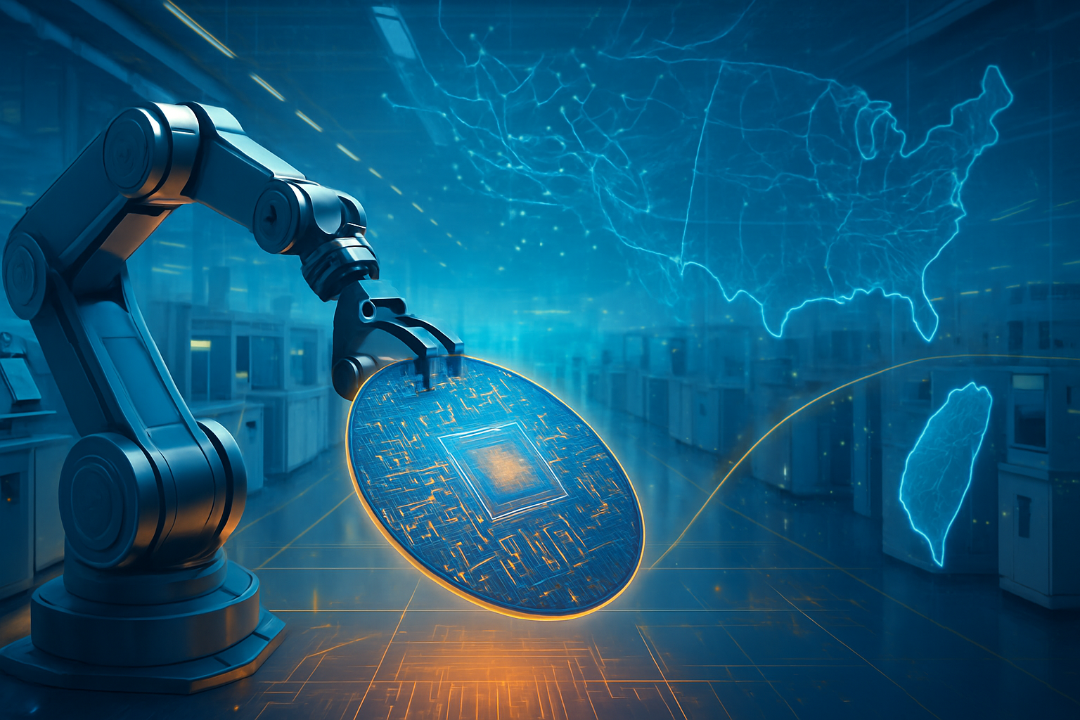
Blog

  • Semiconductor Sector Surges on AI Demand: Penguin Solutions Leads with Strong ‘Buy’ Rating

    Semiconductor Sector Surges on AI Demand: Penguin Solutions Leads with Strong ‘Buy’ Rating

    The global semiconductor industry is experiencing an unprecedented boom, driven by the escalating demands of artificial intelligence (AI) and high-performance computing (HPC). This "AI supercycle" is reshaping investment landscapes, with financial analysts closely scrutinizing companies poised to capitalize on this transformative wave. A recent "Buy" rating for Penguin Solutions (NASDAQ: PENG), a key player in integrated computing platforms and memory solutions, serves as a compelling case study, illustrating how robust financial analysis and strategic positioning are informing the health and future prospects of the entire sector. As of October 2025, the outlook for semiconductor companies, especially those deeply embedded in AI infrastructure, remains overwhelmingly positive, reflecting a pivotal moment in technological advancement.

    The Financial Pulse of Innovation: Penguin Solutions' Strategic Advantage

    Penguin Solutions (NASDAQ: PENG) has consistently garnered "Buy" or "Moderate Buy" ratings from leading analyst firms throughout late 2024 and extending into late 2025, with firms like Rosenblatt Securities, Needham & Company LLC, and Stifel reiterating their optimistic outlooks. In a notable move in October 2025, Rosenblatt significantly raised its price target for Penguin Solutions to $36.00, anticipating the company will exceed consensus estimates due to stronger-than-expected memory demand and pricing. This confidence is rooted in several strategic and financial pillars that underscore Penguin Solutions' critical role in the AI ecosystem.

    At the core of Penguin Solutions' appeal is its laser focus on AI and HPC. The company's Advanced Computing segment, which designs integrated computing platforms for these demanding applications, is a primary growth engine. Analysts like Stifel project this segment to grow by over 20% in fiscal year 2025, propelled by customer and product expansion, an enhanced go-to-market strategy, and a solid sales baseline from a key hyperscaler customer, Meta Platforms (NASDAQ: META). Furthermore, its Integrated Memory segment is experiencing a surge in demand for specialty memory products vital for AI workloads, bolstered by the successful launch of DDR5 CXL Add-in Card products that address the rising need for high-speed memory in AI and in-memory database deployments.

    The company's financial performance further validates these "Buy" ratings. For Q2 Fiscal Year 2025, reported on April 4, 2025, Penguin Solutions announced net sales of $366 million, a robust 28.3% year-over-year increase. Its non-GAAP diluted EPS surged to $0.52 from $0.27 in the prior year. The company ended Fiscal Year 2024 with $1.17 billion in total revenue and a record non-GAAP gross margin of 31.9%. Analysts project double-digit revenue growth for FY25 and EPS between $1.50-$1.90. Moreover, strategic partnerships, such as a planned collaboration with SK Telecom to drive global growth and innovation, and existing work with Dell Technologies (NYSE: DELL) on AI-optimized hardware, solidify its market position. With a forward price-to-earnings (P/E) multiple of 11x in late 2024, significantly lower than the U.S. semiconductor industry average of 39x, many analysts consider the stock undervalued, presenting a compelling investment opportunity within a booming market.

    Reshaping the AI Landscape: Implications for Tech Giants and Startups

    The positive outlook for companies like Penguin Solutions has profound implications across the AI and broader tech industry. Semiconductor advancements are the bedrock upon which all AI innovation is built, meaning a healthy and growing chip sector directly fuels the capabilities of AI companies, tech giants, and nascent startups alike. Companies that provide the foundational hardware, such as Penguin Solutions, are direct beneficiaries of the "insatiable hunger" for computational power.

    Major AI labs and tech giants, including NVIDIA (NASDAQ: NVDA), Advanced Micro Devices (NASDAQ: AMD), and Intel (NASDAQ: INTC), are in a race to develop more powerful and efficient AI chips. Penguin Solutions, through its integrated computing platforms and memory solutions, plays a crucial supporting role, providing essential components and infrastructure that enable these larger players to deploy and scale their AI models. Its partnerships with companies like Dell Technologies (NYSE: DELL) and integration of NVIDIA and AMD GPU technology into its OriginAI infrastructure exemplify this symbiotic relationship. The enhanced capabilities offered by companies like Penguin Solutions allow AI startups to access cutting-edge hardware without the prohibitive costs of developing everything in-house, fostering innovation and reducing barriers to entry.

    The competitive landscape is intensely dynamic. Companies that can consistently deliver advanced, AI-optimized silicon and integrated solutions will gain significant strategic advantages. A strong performer like Penguin Solutions can disrupt existing products or services by offering more efficient or specialized alternatives, pushing competitors to accelerate their own R&D. Market positioning is increasingly defined by the ability to cater to specific AI workloads, whether it's high-performance training in data centers or efficient inference at the edge. The success of companies in this segment directly translates into accelerated AI development, impacting everything from autonomous vehicles and medical diagnostics to generative AI applications and scientific research.

    The Broader Significance: Fueling the AI Supercycle

    The investment trends and analyst confidence in semiconductor companies like Penguin Solutions are not isolated events; they are critical indicators of the broader AI landscape's health and trajectory. The current period is widely recognized as an "AI supercycle," characterized by unprecedented demand for the computational horsepower necessary to train and deploy increasingly complex AI models. Semiconductors are the literal building blocks of this revolution, making the sector's performance a direct proxy for the pace of AI advancement.

    The sheer scale of investment in semiconductor manufacturing and R&D underscores the industry's strategic importance. Global capital expenditures are projected to reach $185 billion in 2025, reflecting a significant expansion in manufacturing capacity. This investment is not just about producing more chips; it's about pushing the boundaries of what's technologically possible, with a substantial portion dedicated to advanced process development (e.g., 2nm and 3nm) and advanced packaging. This technological arms race is essential for overcoming the physical limitations of current silicon and enabling the next generation of AI capabilities.

    While the optimism is high, the wider significance also encompasses potential concerns. Geopolitical tensions, particularly US-China relations and export controls, continue to introduce complexities and drive efforts toward geographical diversification and reshoring of manufacturing capacity. Supply chain vulnerabilities, though improved, remain a persistent consideration. Comparisons to previous tech milestones, such as the dot-com boom or the mobile revolution, highlight the transformative potential of AI, but also serve as a reminder of the industry's inherent cyclicality and the importance of sustainable growth. The current surge, however, appears to be driven by fundamental, long-term shifts in how technology is developed and consumed, suggesting a more enduring impact than previous cycles.

    Future Developments: The Road Ahead for AI Silicon

    Looking ahead, the semiconductor industry is poised for continuous, rapid evolution, largely dictated by the escalating demands of AI. Experts predict that the AI chip market alone could exceed $150 billion in 2025, with some forecasts suggesting it could reach over $400 billion by 2030. This growth will be fueled by several key developments.

    Near-term, we can expect a relentless pursuit of higher performance and greater energy efficiency in AI processors, including more specialized GPUs, custom ASICs, and advanced neural processing units (NPUs) for edge devices. High Bandwidth Memory (HBM) will become increasingly critical, with companies like Micron Technology (NASDAQ: MU) significantly boosting CapEx for HBM production. Advanced packaging technologies, such as 3D stacking, will be crucial for integrating more components into smaller footprints, reducing latency, and increasing overall system performance. The demand for chips in data centers, particularly for compute and memory, is projected to grow by 36% in 2025, signaling a continued build-out of AI infrastructure.

    Long-term, the industry will focus on addressing challenges such as the rising costs of advanced fabs, the global talent shortage, and the complexities of manufacturing at sub-2nm nodes. Innovations in materials science and novel computing architectures, including neuromorphic computing and quantum computing, are on the horizon, promising even more radical shifts in how AI is processed. Experts predict that the semiconductor market will reach $1 trillion by 2030, driven not just by AI, but also by the pervasive integration of AI into automotive, IoT, and next-generation consumer electronics, including augmented and virtual reality devices. The continuous cycle of innovation in silicon will unlock new applications and use cases that are currently unimaginable, pushing the boundaries of what AI can achieve.

    A New Era: The Enduring Impact of Semiconductor Investment

    The "Buy" rating for Penguin Solutions (NASDAQ: PENG) and the broader investment trends in the semiconductor sector underscore a pivotal moment in the history of artificial intelligence. The key takeaway is clear: the health and growth of the semiconductor industry are inextricably linked to the future of AI. Robust financial analysis, focusing on technological leadership, strategic partnerships, and strong financial performance, is proving instrumental in identifying companies that will lead this charge.

    This development signifies more than just market optimism; it represents a fundamental acceleration of AI capabilities across all sectors. The continuous innovation in silicon is not just about faster computers; it's about enabling more intelligent systems, more efficient processes, and entirely new paradigms of interaction and discovery. The industry's commitment to massive capital expenditures and R&D, despite geopolitical headwinds and manufacturing complexities, reflects a collective belief in the transformative power of AI.

    In the coming weeks and months, observers should closely watch for further announcements regarding new chip architectures, expansions in manufacturing capacity, and strategic collaborations between chipmakers and AI developers. The performance of key players like Penguin Solutions will serve as a barometer for the broader AI supercycle, dictating the pace at which AI integrates into every facet of our lives. The current period is not merely a boom; it is the foundational laying of an AI-powered future, with semiconductors as its indispensable cornerstone.


    This content is intended for informational purposes only and represents analysis of current AI developments.

    TokenRing AI delivers enterprise-grade solutions for multi-agent AI workflow orchestration, AI-powered development tools, and seamless remote collaboration platforms. For more information, visit https://www.tokenring.ai/.

  • Silicon’s Green Revolution: How Advanced Chips are Powering the Renewable Energy Transition

    Silicon’s Green Revolution: How Advanced Chips are Powering the Renewable Energy Transition

    The global push towards a sustainable future is accelerating, and at its core lies an often-unsung hero: the semiconductor industry. Far from being merely the engine of our digital lives, advancements in chip technology are now proving indispensable in the renewable energy transition, driving unprecedented progress in how we generate, store, and manage sustainable power. This silent revolution, particularly propelled by emerging materials like organic semiconductors, is fundamentally reshaping the landscape of green energy solutions, promising a future where clean power is not only efficient but also ubiquitous and affordable.

    This pivotal role of semiconductors extends across the entire renewable energy ecosystem, from maximizing the efficiency of solar panels and wind turbines to enabling sophisticated battery management systems and intelligent smart grids. The immediate significance of these developments cannot be overstated; they are directly accelerating the adoption of renewable energy, enhancing grid resilience, and dramatically reducing the cost and accessibility barriers that have historically hindered widespread green energy deployment. As the world grapples with climate change and escalating energy demands, the continuous innovation within chip technology stands as a critical enabler for a truly sustainable future.

    Organic Semiconductors: A Technical Leap Towards Ubiquitous Green Energy

    The technical landscape of renewable energy is being profoundly reshaped by advancements in semiconductor technology, with organic semiconductors emerging as a particularly exciting frontier. Unlike traditional silicon-based chips, organic semiconductors are carbon-based molecules or polymers that offer a unique blend of properties, setting them apart as a game-changer for sustainable solutions.

    A significant breakthrough in organic solar cells (OSCs) has been the development of Non-Fullerene Acceptors (NFAs). These novel materials have dramatically boosted power conversion efficiencies, with laboratory results now approaching and even exceeding 19% in some instances. This is a crucial leap, as earlier organic solar cells often struggled with lower efficiencies, typically around 11%. NFAs address the challenge of exciton binding – where electron-hole pairs formed after light absorption are tightly bound – by facilitating more efficient charge separation. Furthermore, extensive molecular engineering allows researchers to precisely tune the band gap and other electronic properties of these materials, optimizing light absorption and charge transport. This design flexibility extends to creating new organic molecules, such as P3TTM, that exhibit quantum mechanical behaviors previously seen only in inorganic materials, potentially simplifying solar panel construction. Advanced device architectures, including bulk heterojunctions (BHJs) and multi-junction cells, are also being employed to maximize light capture across the solar spectrum and overcome the inherent short exciton diffusion lengths in organic materials.

    These technical specifications highlight the distinct advantages of organic semiconductors. Their inherent flexibility and lightweight nature mean they can be deposited onto flexible substrates using low-cost, low-temperature, solution-based processing methods like roll-to-roll printing. This contrasts sharply with the energy-intensive, high-temperature processes required for crystalline silicon. While commercial crystalline silicon cells typically boast efficiencies between 20% and 25%, the rapid improvement in organic solar cells, coupled with their semi-transparency and tunable properties, opens doors for novel applications like solar windows and integration into curved surfaces, which are impossible with rigid silicon. However, challenges remain, particularly regarding their shorter lifespan and lower charge carrier mobility compared to silicon, areas where active research is focused on improving stability under real-world conditions.

    The initial reactions from the AI research community and industry experts are a mix of optimism and pragmatism. There's widespread recognition of organic semiconductors as a "next-generation technology for a greener future" due to their sustainability, low fabrication cost, and diverse performance capabilities. Crucially, the AI community is actively contributing to this field, leveraging machine learning to accelerate the discovery of new materials, significantly reducing the experimental cycles needed for breakthroughs. Experts emphasize that while efficiency is important, the primary focus is now shifting towards enhancing long-term stability, scalability, and practical integration. The potential for low-cost, mass-produced plastic solar cells with a low embedded energy footprint is seen as a major market disruptor, although widespread commercial use in large-scale solar panels is still in its developmental stages, with existing applications primarily in consumer electronics displays.

    Corporate Fortunes and Competitive Shifts in the Green Chip Era

    The advent of advanced semiconductor technologies, particularly organic semiconductors, is poised to trigger significant shifts in corporate fortunes and reshape competitive landscapes across the tech and energy sectors. This revolution presents immense opportunities for agile innovators while demanding strategic recalibration from established giants.

    Companies specializing in Organic Photovoltaics (OPVs) and their material components are at the forefront of this benefit. Innovators like Heliatek GmbH, a pioneer in flexible organic solar films, are carving out niches in building-integrated photovoltaics (BIPV), automotive applications, and consumer electronics. Similarly, BELECTRIC OPV GmbH and ASCA are leveraging printed photovoltaic technology for customizable modules in smart textiles and architectural designs. Material specialists such as Novaled and Epishine are crucial, providing the high-performance organic materials and focusing on scalability for various appliances. Even traditional solar panel manufacturers like JinkoSolar (NYSE: JKS) and Vikram Solar could strategically integrate these technologies to diversify their offerings and tap into new markets. Beyond solar, the enhanced power management capabilities enabled by efficient organic semiconductors could indirectly benefit wind power giants like Vestas (CPH: VWS) and major Electric Vehicle (EV) manufacturers by optimizing energy flow and battery life.

    The competitive implications for major chip manufacturers and tech giants are profound. While organic semiconductors challenge the long-standing dominance of silicon due to their flexibility, lightweight nature, and lower production costs, they also present immense opportunities for tech titans. Companies like Apple (NASDAQ: AAPL), Google (NASDAQ: GOOGL), Samsung (KRX: 005930), and Amazon (NASDAQ: AMZN) stand to benefit significantly from integrating thin, flexible, and even transparent organic solar cells into consumer electronics, enabling self-charging capabilities and extended battery life for devices ranging from smartphones to VR headsets. This could lead to sleeker designs, enhanced product differentiation, and potentially transparent solar-harvesting displays. However, traditional semiconductor manufacturers must adapt. The shift towards more environmentally friendly, solution-based manufacturing processes for organic semiconductors could reduce reliance on the complex and often vulnerable global silicon supply chain. Major players may need to invest heavily in R&D, forge strategic partnerships, or acquire startups specializing in organic materials to secure intellectual property and manufacturing capabilities in this evolving domain. Material science giants like Merck KGaA (ETR: MRK), BASF SE (ETR: BAS), and Sumitomo Chemical (TYO: 4005) are already focusing on material diversification to capitalize on this trend.

    The disruptive potential of organic semiconductors is already evident in display technology, where Organic Light-Emitting Diodes (OLEDs) have largely supplanted Liquid Crystal Displays (LCDs) in small to medium-sized applications and dominate the premium television market. Companies like Samsung Display Co., Ltd. and LG Display Co., Ltd. (KRX: 034220) have been key disruptors here. Looking ahead, flexible, transparent, and ultra-light OPV films could disrupt traditional rooftop solar installations by enabling energy harvesting from unconventional surfaces like windows or curtains, creating entirely new markets. For low-power Internet of Things (IoT) devices, integrated organic solar cells could eliminate the need for conventional batteries, simplifying deployment and maintenance. Furthermore, Organic Thin-Film Transistors (OTFTs) are paving the way for mechanically flexible and foldable electronic products, leading to innovations like electronic paper and "smart" clothing. Companies that strategically invest in these areas will gain significant advantages in product differentiation, sustainability branding, and cost-effectiveness, potentially creating new market segments and securing robust intellectual property.

    A Broader Horizon: Integrating AI and Sustainability with Organic Chips

    The rise of organic semiconductors extends far beyond incremental improvements in renewable energy; it signifies a profound shift in the broader AI landscape and global sustainability efforts. This technology is not merely an alternative but a crucial enabler for a future where AI is more pervasive, efficient, and environmentally responsible.

    In the AI landscape, organic semiconductors are poised to facilitate a new generation of hardware. Their inherent flexibility and low-power characteristics make them ideal for the burgeoning fields of wearable AI, smart textiles, and implantable medical devices. Imagine biosensors seamlessly integrated into clothing for continuous health monitoring or flexible displays that adapt to any surface. Crucially, organic semiconductors are vital for low-power and edge AI applications, where processing occurs closer to the data source rather than in distant data centers. This reduces latency and energy consumption, critical for the proliferation of IoT devices. Furthermore, organic electronics hold immense potential for neuromorphic computing, which aims to mimic the human brain's structure and function. By enabling components that integrate sensing, memory, and processing—often separate in traditional systems—organic semiconductors can lead to significantly more energy-efficient and high-performing AI hardware. Paradoxically, AI itself is playing a pivotal role in accelerating this development, with machine learning algorithms rapidly discovering and optimizing new organic materials, significantly shortening the traditional trial-and-error approach in materials science.

    The societal and environmental impacts are equally transformative. Socially, biocompatible and flexible organic semiconductors promise to revolutionize healthcare with advanced monitoring and diagnostics, including innovative treatments like photovoltaic retinal prostheses. Their printability and lower production costs could also lead to more affordable and accessible electronics, helping to bridge technological divides globally. Environmentally, organic semiconductors offer a significant reduction in carbon footprint. Unlike conventional silicon, which demands energy-intensive, high-temperature manufacturing and often involves toxic metals, organic materials can be produced using low-temperature, less energy-intensive processes. Many are also biocompatible and biodegradable, offering a potential solution to the escalating problem of electronic waste (e-waste) by being recyclable like plastics. Organic photovoltaics (OPVs) provide a greener alternative to traditional silicon solar cells, utilizing earth-abundant materials and enabling seamless integration into buildings and vehicles through their transparent and flexible properties, expanding solar energy harvesting possibilities.

    However, potential concerns remain. While efficiency has improved dramatically, organic solar cells still generally have shorter lifespans and lower power conversion efficiencies compared to crystalline silicon, with degradation due to environmental factors being a persistent challenge. Scalability of manufacturing for high-performance organic devices also needs further optimization. Moreover, the energy consumption of the AI tools used to discover these materials presents an interesting paradox, underscoring the need for energy-efficient AI practices. Geopolitical factors, resource constraints, and trade restrictions impacting the broader semiconductor industry could also affect the supply chain and adoption of organic semiconductors. When compared to previous AI and energy milestones, organic semiconductors represent a fundamental paradigm shift. In AI, they move beyond the limitations of rigid, energy-intensive silicon, enabling a future of pervasive, low-power, and flexible intelligence. In energy, they herald a "greener" third wave of solar technology, moving beyond the rigidity and e-waste concerns of traditional silicon panels towards a future where energy harvesting is seamlessly integrated into our built environment, akin to how the invention of the electric generator revolutionized energy distribution. This evolution signifies a concerted move towards sustainable technological progress.

    The Road Ahead: Unlocking the Full Potential of Organic Chips for Green Energy

    The trajectory of organic semiconductors in renewable energy is one of continuous innovation and expanding horizons. Both near-term and long-term developments promise to solidify their role as a cornerstone of sustainable power, although significant challenges must still be navigated for widespread commercial viability.

    In the near term (the next 1-5 years), we can expect to see organic photovoltaic (OPV) cells push laboratory power conversion efficiencies (PCEs) beyond the 20% mark for single-junction cells, building on the success of non-fullerene acceptors (NFAs). This will bring them increasingly closer to the performance of traditional silicon. A critical focus will also be on significantly improving long-term operational stability and durability under diverse environmental conditions, with ongoing research in phase stabilization and compositional engineering. Furthermore, the industry will concentrate on scaling up manufacturing processes from laboratory to commercial-scale production, leveraging solution-based methods like roll-to-roll printing to reduce costs and complexity. A deeper understanding of fundamental electronic processes, such as "entropy-driven charge separation" in NFAs, will continue to drive these improvements.

    Looking further ahead, the long-term vision includes the development of highly efficient hybrid organic-perovskite tandem cells, designed to capture an even broader spectrum of light. Advanced material design, process refinement, and interface engineering will further augment the efficiency and durability of OPVs. Crucially, Artificial Intelligence (AI), particularly machine learning, is predicted to play a paramount role in accelerating the discovery and optimization of new organic solar materials and device designs, analyzing vast datasets to predict PCE and stability with unprecedented speed. This synergistic relationship between AI and material science will be key to unlocking the full potential of organic semiconductors. The widespread adoption of transparent and flexible organic solar cells for building-integrated photovoltaics (BIPV), smart windows, and self-powered smart textiles is also on the horizon, enabling a truly distributed energy generation model. Beyond solar, organic thermoelectrics (OTEs) are being developed to convert waste heat into electricity, offering flexible and environmentally friendly solutions for waste heat recovery in various applications.

    These unique properties—flexibility, lightweight nature, transparency, and low-cost manufacturing—open up a vast array of potential applications. Transparent organic solar cells can be seamlessly integrated into windows and facades, transforming buildings into active energy generators. Flexible organic films can power wearable devices and smart textiles, providing portable energy for consumer electronics. EVs could incorporate organic solar cells into sunroofs or body panels to extend range. Their adaptability makes them ideal for off-grid and remote power solutions, while semi-transparent versions could enable "agrivoltaics" in greenhouses, generating electricity while supporting plant growth. Experts predict that organic solar cells will carve out a distinct market niche rather than directly replacing silicon for large utility-scale installations. Their value will lie in their adaptability, aesthetic appeal, and lower installation and transportation costs. The future promises continued rapid evolution, driven by ongoing research and the accelerating influence of AI, leading to a broader range of applications and a strong focus on sustainability. However, challenges in narrowing the efficiency gap with silicon, ensuring long-term stability and durability, and achieving cost-effective large-scale manufacturing remain critical hurdles that must be addressed for organic semiconductors to achieve widespread commercial viability.

    A Sustainable Future Powered by Advanced Semiconductors

    The semiconductor industry's pivotal role in the renewable energy transition, particularly through the advancements in organic semiconductor technology, is a narrative of profound significance for both AI and global sustainability. Key takeaways highlight that semiconductors are not just components but the foundational infrastructure enabling efficient green energy generation, storage, and management. Organic semiconductors, with their inherent flexibility, lightweight properties, and potential for low-cost, environmentally friendly manufacturing, are emerging as a transformative force, promising to democratize access to clean energy and reduce the ecological footprint of electronics.

    This development marks a crucial juncture in both AI history and the energy transition. For AI, it paves the way for a new generation of low-power, flexible, and pervasive intelligent systems, from wearable AI to neuromorphic computing, moving beyond the limitations of rigid silicon. For energy, it represents a "greener" third wave of solar technology, offering versatile and integrated energy harvesting solutions that can seamlessly blend into our built environment. The long-term impact is a fundamental shift towards a future where technology is inherently more sustainable, with high-performance computing coexisting harmoniously with environmental responsibility.

    In the coming weeks and months, watch for continued breakthroughs in the efficiency and stability of organic photovoltaics, particularly as they scale to larger modules. Keep an eye on new material science discoveries, especially in non-fullerene acceptors, and advancements in solution-based processing and printing techniques that will enable low-cost, large-scale manufacturing. The synergistic role of AI in accelerating the design and discovery of these new materials will be a powerful indicator of progress. Finally, observe the expansion of organic semiconductor applications beyond traditional displays into flexible electronics, smart packaging, IoT devices, transparent solar cells for building integration, and hybrid technologies combining organic layers with inorganic semiconductors to achieve even higher efficiencies. The organic semiconductor market is projected for substantial expansion, signaling a future where these innovative chips are integral to both renewable energy solutions and next-generation AI hardware.

    This content is intended for informational purposes only and represents analysis of current AI developments.

    TokenRing AI delivers enterprise-grade solutions for multi-agent AI workflow orchestration, AI-powered development tools, and seamless remote collaboration platforms.
    For more information, visit https://www.tokenring.ai/.

  • The Silicon Revolution: How AI and Machine Learning Are Forging the Future of Semiconductor Manufacturing

    The Silicon Revolution: How AI and Machine Learning Are Forging the Future of Semiconductor Manufacturing

    The intricate world of semiconductor manufacturing, the bedrock of our digital age, is on the precipice of a transformative revolution, powered by the immediate and profound impact of Artificial Intelligence (AI) and Machine Learning (ML). Far from being a futuristic concept, AI/ML is swiftly becoming an indispensable force, meticulously optimizing every stage of chip production, from initial design to final fabrication. This isn't merely an incremental improvement; it's a crucial evolution for the tech industry, promising to unlock unprecedented efficiencies, accelerate innovation, and dramatically reshape the competitive landscape.

    The insatiable global demand for faster, smaller, and more energy-efficient chips, coupled with the escalating complexity and cost of traditional manufacturing processes, has made the integration of AI/ML an urgent imperative. AI-driven solutions are already slashing chip design cycles from months to mere hours or days, automating complex tasks, optimizing circuit layouts for superior performance and power efficiency, and rigorously enhancing verification and testing to detect design flaws with unprecedented accuracy. Simultaneously, in the fabrication plants, AI/ML is a game-changer for yield optimization, enabling predictive maintenance to avert costly downtime, facilitating real-time process adjustments for higher precision, and employing advanced defect detection systems that can identify imperfections with near-perfect accuracy, often reducing yield detraction by up to 30%. This pervasive optimization across the entire value chain is not just about making chips better and faster; it's about securing the future of technological advancement itself, ensuring that the foundational components for AI, IoT, high-performance computing, and autonomous systems can continue to evolve at the pace required by an increasingly digital world.

    Technical Deep Dive: AI's Precision Engineering in Silicon Production

    AI and Machine Learning (ML) are profoundly transforming the semiconductor industry, introducing unprecedented levels of efficiency, precision, and automation across the entire production lifecycle. This paradigm shift addresses the escalating complexities and demands for smaller, faster, and more power-efficient chips, overcoming limitations inherent in traditional, often manual and iterative, approaches. The impact of AI/ML is particularly evident in design, simulation, testing, and fabrication processes.

    In chip design, AI is revolutionizing the field by automating and optimizing numerous traditionally time-consuming and labor-intensive stages. Generative AI models, including Generative Adversarial Networks (GANs) and Variational Autoencoders (VAEs), can create optimized chip layouts, circuits, and architectures, analyzing vast datasets to generate novel, efficient solutions that human designers might not conceive. This significantly streamlines design by exploring a much larger design space, drastically reducing design cycles from months to weeks and cutting design time by 30-50%. Reinforcement Learning (RL) algorithms, famously used by Google to design its Tensor Processing Units (TPUs), optimize chip layout by learning from dynamic interactions, moving beyond traditional rule-based methods to find optimal strategies for power, performance, and area (PPA). AI-powered Electronic Design Automation (EDA) tools, such as Synopsys DSO.ai and Cadence Cerebrus, integrate ML to automate repetitive tasks, predict design errors, and generate optimized layouts, reducing power efficiency by up to 40% and improving design productivity by 3x to 5x. Initial reactions from the AI research community and industry experts hail generative AI as a "game-changer," enabling greater design complexity and allowing engineers to focus on innovation.

    Semiconductor simulation is also being accelerated and enhanced by AI. ML-accelerated physics simulations, powered by technologies from companies like Rescale and NVIDIA (NASDAQ: NVDA), utilize ML models trained on existing simulation data to create surrogate models. This allows engineers to quickly explore design spaces without running full-scale, resource-intensive simulations for every configuration, drastically reducing computational load and accelerating R&D. Furthermore, AI for thermal and power integrity analysis predicts power consumption and thermal behavior, optimizing chip architecture for energy efficiency. This automation allows for rapid iteration and identification of optimal designs, a capability particularly valued for developing energy-efficient chips for AI applications.

    In semiconductor testing, AI is improving accuracy, reducing test time, and enabling predictive capabilities. ML for fault detection, diagnosis, and prediction analyzes historical test data to predict potential failure points, allowing for targeted testing and reducing overall test time. Machine learning models, such as Artificial Neural Networks (ANNs) and Support Vector Machines (SVMs), can identify complex and subtle fault patterns that traditional methods might miss, achieving up to 95% accuracy in defect detection. AI algorithms also optimize test patterns, significantly reducing the time and expertise needed for manual development. Synopsys TSO.ai, an AI-driven ATPG (Automatic Test Pattern Generation) solution, consistently reduces pattern count by 20% to 25%, and in some cases over 50%. Predictive maintenance for test equipment, utilizing RNNs and other time-series analysis models, forecasts equipment failures, preventing unexpected breakdowns and improving overall equipment effectiveness (OEE). The test community, while initially skeptical, is now embracing ML for its potential to optimize costs and improve quality.

    Finally, in semiconductor fabrication processes, AI is dramatically enhancing efficiency, precision, and yield. ML for process control and optimization (e.g., lithography, etching, deposition) provides real-time feedback and control, dynamically adjusting parameters to maintain optimal conditions and reduce variability. AI has been shown to reduce yield detraction by up to 30%. AI-powered computer vision systems, trained with Convolutional Neural Networks (CNNs), automate defect detection by analyzing high-resolution images of wafers, identifying subtle defects such as scratches, cracks, or contamination that human inspectors often miss. This offers automation, consistency, and the ability to classify defects at pixel size. Reinforcement Learning for yield optimization and recipe tuning allows models to learn decisions that minimize process metrics by interacting with the manufacturing environment, offering faster identification of optimal experimental conditions compared to traditional methods. Industry experts see AI as central to "smarter, faster, and more efficient operations," driving significant improvements in yield rates, cost savings, and production capacity.

    Corporate Impact: Reshaping the Semiconductor Ecosystem

    The integration of Artificial Intelligence (AI) into semiconductor manufacturing is profoundly reshaping the industry, creating new opportunities and challenges for AI companies, tech giants, and startups alike. This transformation impacts everything from design and production efficiency to market positioning and competitive dynamics.

    A broad spectrum of companies across the semiconductor value chain stands to benefit. AI chip designers and manufacturers like NVIDIA (NASDAQ: NVDA), AMD (NASDAQ: AMD), and to a lesser extent, Intel (NASDAQ: INTC), are primary beneficiaries due to the surging demand for high-performance GPUs and AI-specific processors. NVIDIA, with its powerful GPUs and CUDA ecosystem, holds a strong lead. Leading foundries and equipment suppliers such as Taiwan Semiconductor Manufacturing Company (TSMC) (NYSE: TSM) and Samsung Electronics (KRX: 005930) are crucial, manufacturing advanced chips and benefiting from increased capital expenditure. Equipment suppliers like ASML (NASDAQ: ASML), Lam Research (NASDAQ: LRCX), and Applied Materials (NASDAQ: AMAT) also see increased demand. Electronic Design Automation (EDA) companies like Synopsys (NASDAQ: SNPS) and Cadence (NASDAQ: CDNS) are leveraging AI to streamline chip design, with Synopsys.ai Copilot integrating Azure's OpenAI service. Hyperscalers and Cloud Providers such as Alphabet (NASDAQ: GOOGL), Microsoft (NASDAQ: MSFT), Amazon (NASDAQ: AMZN), Meta Platforms (NASDAQ: META), and Oracle (NYSE: ORCL) are investing heavily in custom AI accelerators to optimize cloud services and reduce reliance on external suppliers. Companies specializing in custom AI chips and connectivity like Broadcom (NASDAQ: AVGO) and Marvell Technology Group (NASDAQ: MRVL), along with those tailoring chips for specific AI applications such as Analog Devices (NASDAQ: ADI), Qualcomm (NASDAQ: QCOM), and ARM Holdings (NASDAQ: ARM), are also capitalizing on the AI boom. AI is even lowering barriers to entry for semiconductor startups by providing cloud-based design tools, democratizing access to advanced resources.

    The competitive landscape is undergoing significant shifts. Major tech giants are increasingly designing their own custom AI chips (e.g., Google's TPUs, Microsoft's Maia), a strategy aiming to optimize performance, reduce dependence on external suppliers, and mitigate geopolitical risks. While NVIDIA maintains a strong lead, AMD is aggressively competing with its GPU offerings, and Intel is making strategic moves with its Gaudi accelerators and expanding its foundry services. The demand for advanced chips (e.g., 2nm, 3nm process nodes) is intense, pushing foundries like TSMC and Samsung into fierce competition for leadership in manufacturing capabilities and advanced packaging technologies. Geopolitical tensions and export controls are also forcing strategic pivots in product development and market segmentation.

    AI in semiconductor manufacturing introduces several disruptive elements. AI-driven tools can compress chip design and verification times from months or years to days, accelerating time-to-market. Cloud-based design tools, amplified by AI, democratize chip design for smaller companies and startups. AI-driven design is paving the way for specialized processors tailored for specific applications like edge computing and IoT. The vision of fully autonomous manufacturing facilities could significantly reduce labor costs and human error, reshaping global manufacturing strategies. Furthermore, AI enhances supply chain resilience through predictive maintenance, quality control, and process optimization. While AI automates many tasks, human creativity and architectural insight remain critical, shifting engineers from repetitive tasks to higher-level innovation.

    Companies are adopting various strategies to position themselves advantageously. Those with strong intellectual property in AI-specific architectures and integrated hardware-software ecosystems (like NVIDIA's CUDA) are best positioned. Specialization and customization for specific AI applications offer a strategic advantage. Foundries with cutting-edge process nodes and advanced packaging technologies gain a significant competitive edge. Investing in and developing AI-driven EDA tools is crucial for accelerating product development. Utilizing AI for supply chain optimization and resilience is becoming a necessity to reduce costs and ensure stable production. Cloud providers offering AI-as-a-Service, powered by specialized AI chips, are experiencing surging demand. Continuous investment in R&D for novel materials, architectures, and energy-efficient designs is vital for long-term competitiveness.

    A Broader Lens: AI's Transformative Role in the Digital Age

    The integration of Artificial Intelligence (AI) into semiconductor manufacturing optimization marks a pivotal shift in the tech industry, driven by the escalating complexity of chip design and the demand for enhanced efficiency and performance. This profound impact extends across various facets of the manufacturing lifecycle, aligning with broader AI trends and introducing significant societal and industrial changes, alongside potential concerns and comparisons to past technological milestones.

    AI is revolutionizing semiconductor manufacturing by bringing unprecedented levels of precision, efficiency, and automation to traditionally complex and labor-intensive processes. This includes accelerating chip design and verification, optimizing manufacturing processes to reduce yield loss by up to 30%, enabling predictive maintenance to minimize unscheduled downtime, and enhancing defect detection and quality control with up to 95% accuracy. Furthermore, AI optimizes supply chain and logistics, and improves energy efficiency within manufacturing facilities.

    AI's role in semiconductor manufacturing optimization is deeply embedded in the broader AI landscape. There's a powerful feedback loop where AI's escalating demand for computational power drives the need for more advanced, smaller, faster, and more energy-efficient semiconductors, while these semiconductor advancements, in turn, enable even more sophisticated AI applications. This application fits squarely within the Fourth Industrial Revolution (Industry 4.0), characterized by highly digitized, connected, and increasingly autonomous smart factories. Generative AI (Gen AI) is accelerating innovation by generating new chip designs and improving defect categorization. The increasing deployment of Edge AI requires specialized, low-power, high-performance chips, further driving innovation in semiconductor design. The AI for semiconductor manufacturing market is experiencing robust growth, projected to expand significantly, demonstrating its critical role in the industry's future.

    The pervasive adoption of AI in semiconductor manufacturing carries far-reaching implications for the tech industry and society. It fosters accelerated innovation, leading to faster development of cutting-edge technologies and new chip architectures, including AI-specific chips like Tensor Processing Units and FPGAs. Significant cost savings are achieved through higher yields, reduced waste, and optimized energy consumption. Improved demand forecasting and inventory management contribute to a more stable and resilient global semiconductor supply chain. For society, this translates to enhanced performance in consumer electronics, automotive applications, and data centers. Crucially, without increasingly powerful and efficient semiconductors, the progress of AI across all sectors (healthcare, smart cities, climate modeling, autonomous systems) would be severely limited.

    Despite the numerous benefits, several critical concerns accompany this transformation. High implementation costs and technical challenges are associated with integrating AI solutions with existing complex manufacturing infrastructures. Effective AI models require vast amounts of high-quality data, but data scarcity, quality issues, and intellectual property concerns pose significant hurdles. Ensuring the accuracy, reliability, and explainability of AI models is crucial in a field demanding extreme precision. The shift towards AI-driven automation may lead to job displacement in repetitive tasks, necessitating a workforce with new skills in AI and data science, which currently presents a significant skill gap. Ethical concerns regarding AI's misuse in areas like surveillance and autonomous weapons also require responsible development. Furthermore, semiconductor manufacturing and large-scale AI model training are resource-intensive, consuming vast amounts of energy and water, posing environmental challenges. The AI semiconductor boom is also a "geopolitical flashpoint," with strategic importance and implications for global power dynamics.

    AI in semiconductor manufacturing optimization represents a significant evolutionary step, comparable to previous AI milestones and industrial revolutions. As traditional Moore's Law scaling approaches its physical limits, AI-driven optimization offers alternative pathways to performance gains, marking a fundamental shift in how computational power is achieved. This is a core component of Industry 4.0, emphasizing human-technology collaboration and intelligent, autonomous factories. AI's contribution is not merely an incremental improvement but a transformative shift, enabling the creation of complex chip architectures that would be infeasible to design using traditional, human-centric methods, pushing the boundaries of what is technologically possible. The current generation of AI, particularly deep learning and generative AI, is dramatically accelerating the pace of innovation in highly complex fields like semiconductor manufacturing.

    The Road Ahead: Future Developments and Expert Outlook

    The integration of Artificial Intelligence (AI) is rapidly transforming semiconductor manufacturing, moving beyond theoretical applications to become a critical component in optimizing every stage of production. This shift is driven by the increasing complexity of chip designs, the demand for higher precision, and the need for greater efficiency and yield in a highly competitive global market. Experts predict a dramatic acceleration of AI/ML adoption, projecting annual value generation of $35 billion to $40 billion within the next two to three years and a market expansion from $46.3 billion in 2024 to $192.3 billion by 2034.

    In the near term (1-3 years), AI is expected to deliver significant advancements. Predictive maintenance (PDM) systems will become more prevalent, analyzing real-time sensor data to anticipate equipment failures, potentially increasing tool availability by up to 15% and reducing unplanned downtime by as much as 50%. AI-powered computer vision and deep learning models will enhance the speed and accuracy of detecting minute defects on wafers and masks. AI will also dynamically adjust process parameters in real-time during manufacturing steps, leading to greater consistency and fewer errors. AI models will predict low-yielding wafers proactively, and AI-powered automated material handling systems (AMHS) will minimize contamination risks in cleanrooms. AI-powered Electronic Design Automation (EDA) tools will automate repetitive design tasks, significantly shortening time-to-market.

    Looking further ahead into long-term developments (3+ years), AI's role will expand into more sophisticated and transformative applications. AI will drive more sophisticated computational lithography, enabling even smaller and more complex circuit patterns. Hybrid AI models, combining physics-based modeling with machine learning, will lead to greater accuracy and reliability in process control. The industry will see the development of novel AI-specific hardware architectures, such as neuromorphic chips, for more energy-efficient and powerful AI processing. AI will play a pivotal role in accelerating the discovery of new semiconductor materials with enhanced properties. Ultimately, the long-term vision includes highly automated or fully autonomous fabrication plants where AI systems manage and optimize nearly all aspects of production with minimal human intervention, alongside more robust and diversified supply chains.

    Potential applications and use cases on the horizon span the entire semiconductor lifecycle. In Design & Verification, generative AI will automate complex chip layout, design optimization, and code generation. For Manufacturing & Fabrication, AI will optimize recipe parameters, manage tool performance, and perform full factory simulations. Companies like TSMC (NYSE: TSM) and Intel (NASDAQ: INTC) are already employing AI for predictive equipment maintenance, computer vision on wafer faults, and real-time data analysis. In Quality Control, AI-powered systems will perform high-precision measurements and identify subtle variations too minute for human eyes. For Supply Chain Management, AI will analyze vast datasets to forecast demand, optimize logistics, manage inventory, and predict supply chain risks with unprecedented precision.

    Despite its immense potential, several significant challenges must be overcome. These include data scarcity and quality, the integration of AI with legacy manufacturing systems, the need for improved AI model validation and explainability, and a significant talent gap in professionals with expertise in both semiconductor engineering and AI/machine learning. High implementation costs, the computational intensity of AI workloads, geopolitical risks, and the need for clear value identification also pose hurdles.

    Experts widely agree that AI is not just a passing trend but a transformative force. Generative AI (GenAI) is considered a "new S-curve" for the industry, poised to revolutionize design, manufacturing, and supply chain management. The exponential growth of AI applications is driving an unprecedented demand for high-performance, specialized AI chips, making AI an indispensable ally in developing cutting-edge semiconductor technologies. The focus will also be on energy efficiency and specialization, particularly for AI in edge devices. McKinsey estimates that AI/ML could generate between $35 billion and $40 billion in annual value for semiconductor companies within the next two to three years.

    The AI-Powered Silicon Future: A New Era of Innovation

    The integration of AI into semiconductor manufacturing optimization is fundamentally reshaping the landscape, driving unprecedented advancements in efficiency, quality, and innovation. This transformation marks a pivotal moment, not just for the semiconductor industry, but for the broader history of artificial intelligence itself.

    The key takeaways underscore AI's profound impact: it delivers enhanced efficiency and significant cost reductions across design, manufacturing, and supply chain management. It drastically improves quality and yield through advanced defect detection and process control. AI accelerates innovation and time-to-market by automating complex design tasks and enabling generative design. Ultimately, it propels the industry towards increased automation and autonomous manufacturing.

    This symbiotic relationship between AI and semiconductors is widely considered the "defining technological narrative of our time." AI's insatiable demand for processing power drives the need for faster, smaller, and more energy-efficient chips, while these semiconductor advancements, in turn, fuel AI's potential across diverse industries. This development is not merely an incremental improvement but a powerful catalyst, propelling the Fourth Industrial Revolution (Industry 4.0) and enabling the creation of complex chip architectures previously infeasible.

    The long-term impact is expansive and transformative. The semiconductor industry is projected to become a trillion-dollar market by 2030, with the AI chip market alone potentially reaching over $400 billion by 2030, signaling a sustained era of innovation. We will likely see more resilient, regionally fragmented global semiconductor supply chains driven by geopolitical considerations. Technologically, disruptive hardware architectures, including neuromorphic designs, will become more prevalent, and the ultimate vision includes fully autonomous manufacturing environments. A significant long-term challenge will be managing the immense energy consumption associated with escalating computational demands.

    In the coming weeks and months, several key areas warrant close attention. Watch for further government policy announcements regarding export controls and domestic subsidies, as nations strive for greater self-sufficiency in chip production. Monitor the progress of major semiconductor fabrication plant construction globally. Observe the accelerated integration of generative AI tools within Electronic Design Automation (EDA) suites and their impact on design cycles. Keep an eye on the introduction of new custom AI chip architectures and intensified competition among major players like NVIDIA (NASDAQ: NVDA), AMD (NASDAQ: AMD), and Intel (NASDAQ: INTC). Finally, look for continued breakthroughs in advanced packaging technologies and High Bandwidth Memory (HBM) customization, crucial for supporting the escalating performance demands of AI applications, and the increasing integration of AI into edge devices. The ongoing synergy between AI and semiconductor manufacturing is not merely a trend; it is a fundamental transformation that promises to redefine technological capabilities and global industrial landscapes for decades to come.

    This content is intended for informational purposes only and represents analysis of current AI developments.

    TokenRing AI delivers enterprise-grade solutions for multi-agent AI workflow orchestration, AI-powered development tools, and seamless remote collaboration platforms. For more information, visit https://www.tokenring.ai/.

  • The Atomic Edge: How Novel Materials Are Forging the Future of AI Chips

    The Atomic Edge: How Novel Materials Are Forging the Future of AI Chips

    The relentless pursuit of computational power, fueled by the explosive growth of artificial intelligence, is pushing the semiconductor industry to its fundamental limits. As traditional silicon-based technologies approach their physical boundaries, a new frontier is emerging: advanced materials science. This critical field is not merely enhancing existing chip designs but is fundamentally redefining what's possible, ushering in an era where novel materials are the key to unlocking unprecedented chip performance, functionality, and energy efficiency. From wide-bandgap semiconductors powering electric vehicles to atomically thin 2D materials promising ultra-fast transistors, the microscopic world of atoms and electrons is now dictating the macroscopic capabilities of our digital future.

    This revolution in materials is poised to accelerate the development of next-generation AI, high-performance computing, and edge devices. By offering superior electrical, thermal, and mechanical properties, these advanced compounds are enabling breakthroughs in processing speed, power management, and miniaturization, directly addressing the insatiable demands of increasingly complex AI models and data-intensive applications. The immediate significance lies in overcoming the bottlenecks that silicon alone can no longer resolve, paving the way for innovations that were once considered theoretical, and setting the stage for a new wave of technological progress across diverse industries.

    Beyond Silicon: A Deep Dive into the Materials Revolution

    The core of this materials revolution lies in moving beyond the inherent limitations of silicon. While silicon has been the bedrock of the digital age, its electron mobility and thermal conductivity are finite, especially as transistors shrink to atomic scales. Novel materials offer pathways to transcend these limits, enabling faster switching speeds, higher power densities, and significantly reduced energy consumption.

    Wide-Bandgap (WBG) Semiconductors are at the forefront of this shift, particularly Gallium Nitride (GaN) and Silicon Carbide (SiC). Unlike silicon, which has a bandgap of 1.1 electron volts (eV), GaN boasts 3.4 eV and SiC 3.3 eV. This wider bandgap translates directly into several critical advantages. Devices made from GaN and SiC can operate at much higher voltages, temperatures, and frequencies without breaking down. This allows for significantly faster switching speeds, which is crucial for power electronics in applications like electric vehicle chargers, 5G infrastructure, and data center power supplies. Their superior thermal conductivity also means less heat generation and more efficient power conversion, directly impacting the energy footprint of AI hardware. For instance, a GaN-based power transistor can switch thousands of times faster than a silicon equivalent, dramatically reducing energy loss. Initial reactions from the power electronics community have been overwhelmingly positive, with widespread adoption in specific niches and a clear roadmap for broader integration.

    Two-Dimensional (2D) Materials represent an even more radical departure from traditional bulk semiconductors. Graphene, a single layer of carbon atoms arranged in a hexagonal lattice, exemplifies this category. Renowned for its extraordinary electron mobility (up to 100 times that of silicon) and thermal conductivity, graphene has long been hailed for its potential in ultra-fast transistors and interconnects. While its lack of an intrinsic bandgap posed challenges for digital logic, recent breakthroughs in engineering semiconducting graphene with useful bandgaps have revitalized its prospects. Other 2D materials, such as Molybdenum Disulfide (MoS2) and other Transition Metal Dichalcogenides (TMDs), also offer unique advantages. MoS2, for example, possesses a stable bandgap nearly twice that of silicon, making it a promising candidate for flexible electronics and next-generation transistors. These materials' atomic-scale thickness is paramount for continued miniaturization, pushing the boundaries of Moore's Law and enabling novel device architectures that can be stacked in 3D configurations without significant performance degradation. The AI research community is particularly interested in 2D materials for neuromorphic computing and edge AI, where ultra-low power and high-density integration are critical.

    Beyond these, Carbon Nanotubes (CNTs) are gaining traction as a more mature 2D technology, offering tunable electrical properties and ultra-high carrier mobilities, with practical transistors already fabricated at sub-10nm scales. Hafnium Oxide is being manipulated to achieve stable ferroelectric properties, enabling co-location of computation and memory on a single chip, drastically reducing energy consumption for AI workloads. Furthermore, Indium-based materials are being developed to facilitate Extreme Ultraviolet (EUV) lithography, crucial for creating smaller, more precise features and enabling advanced 3D circuit production without damaging existing layers. These materials collectively represent a paradigm shift, moving chip design from merely shrinking existing structures to fundamentally reimagining the building blocks themselves.

    Corporate Giants and Nimble Startups: Navigating the New Material Frontier

    The shift towards advanced materials in semiconductor development is not just a technical evolution; it's a strategic battleground with profound implications for AI companies, tech giants, and ambitious startups alike. The race to integrate Gallium Nitride (GaN), Silicon Carbide (SiC), and 2D materials is reshaping competitive landscapes and driving significant investment.

    Leading the charge in GaN and SiC are established power semiconductor players. Companies like Wolfspeed (NYSE: WOLF), formerly Cree, Inc., are dominant in SiC wafers and devices, crucial for electric vehicles and renewable energy. STMicroelectronics N.V. (NYSE: STM) is heavily invested in SiC, expanding production facilities to meet surging automotive demand. Infineon Technologies AG (ETR: IFX) and ON Semiconductor (NASDAQ: ON) are also major players, making significant advancements in both GaN and SiC for power conversion and automotive applications. In the GaN space, specialized firms such as Navitas Semiconductor (NASDAQ: NVTS) and Efficient Power Conversion Corporation (EPC) are challenging incumbents with innovative GaN power ICs, enabling smaller, faster chargers and more efficient power supplies for consumer electronics and data centers. These companies stand to benefit immensely from the growing demand for high-efficiency power solutions, directly impacting the energy footprint of AI infrastructure.

    For major AI labs and tech giants like Google (NASDAQ: GOOGL), Samsung Electronics (KRX: 005930), TSMC (NYSE: TSM), and Intel Corporation (NASDAQ: INTC), the competitive implications are immense. These companies are not just consumers of advanced chips but are also heavily investing in research and development of these materials to enhance their custom AI accelerators (like Google's TPUs) and next-generation processors. The ability to integrate these materials will directly translate to more powerful, energy-efficient AI hardware, providing a significant competitive edge in training massive models and deploying AI at scale. For instance, better power efficiency means lower operating costs for vast data centers running AI workloads, while faster chips enable quicker iterations in AI model development. The race for talent in materials science and semiconductor engineering is intensifying, becoming a critical factor in maintaining leadership.

    This materials revolution also presents a fertile ground for startups. Niche players specializing in custom chip design for AI, IoT, and edge computing, or those developing novel fabrication techniques for 2D materials, can carve out significant market shares. Companies like Graphenea and 2D Materials Pte Ltd are focusing on the commercialization of graphene and other 2D materials, creating foundational components for future devices. However, startups face substantial hurdles, including the capital-intensive nature of semiconductor R&D and manufacturing, which can exceed $15 billion for a cutting-edge fabrication plant. Nevertheless, government initiatives, such as the CHIPS Act, aim to foster innovation and support both established and emerging players in these critical areas. The disruption to existing products is already evident: GaN-based fast chargers are rapidly replacing traditional silicon chargers, and SiC is becoming standard in high-performance electric vehicles, fundamentally altering the market for power electronics and automotive components.

    A New Era of Intelligence: Broader Implications and Future Trajectories

    The fusion of advanced materials science with semiconductor development is not merely an incremental upgrade; it represents a foundational shift that profoundly impacts the broader AI landscape and global technological trends. This revolution is enabling new paradigms of computing, pushing the boundaries of what AI can achieve, and setting the stage for unprecedented innovation.

    At its core, this materials-driven advancement is enabling AI-specific hardware to an extent never before possible. The insatiable demand for processing power for tasks like large language model training and generative AI inference has led to the creation of specialized chips such as Tensor Processing Units (TPUs) and Application-Specific Integrated Circuits (ASICs). Advanced materials allow for greater transistor density, reduced latency, and significantly lower power consumption in these accelerators, directly fueling the rapid progress in AI capabilities. Furthermore, the development of neuromorphic computing, inspired by the human brain, relies heavily on novel materials like phase-change materials and memristive oxides (e.g., hafnium oxide). These materials are crucial for creating devices that mimic synaptic plasticity, allowing for in-memory computation and vastly more energy-efficient AI systems that overcome the limitations of traditional Von Neumann architectures. This shift from general-purpose computing to highly specialized, biologically inspired hardware represents a profound architectural change, akin to the shift from early vacuum tube computers to integrated circuits.

    The wider impacts of this materials revolution are vast. Economically, it fuels a "trillion-dollar sector" of AI and semiconductors, driving innovation, creating new job opportunities, and fostering intense global competition. Technologically, more powerful and energy-efficient semiconductors are accelerating advancements across nearly every sector, from autonomous vehicles and IoT devices to healthcare and industrial automation. AI itself is becoming a critical tool in this process, with AI for AI becoming a defining trend. AI algorithms are now used to predict material properties, optimize chip architectures, and even automate parts of the manufacturing process, significantly reducing R&D time and costs. This symbiotic relationship, where AI accelerates the discovery of the very materials that power its future, was not as prominent in earlier AI milestones and marks a new era of self-referential advancement.

    However, this transformative period is not without its potential concerns. The immense computational power required by modern AI models, even with more efficient hardware, still translates to significant energy consumption, posing environmental and economic challenges. The technical hurdles in designing and manufacturing with these novel materials are enormous, requiring billions of dollars in R&D and sophisticated infrastructure, which can create barriers to entry. There's also a growing skill gap, as the industry demands a workforce proficient in both advanced materials science and AI/data science. Moreover, the extreme concentration of advanced semiconductor design and production among a few key global players (e.g., NVIDIA Corporation (NASDAQ: NVDA), TSMC (NYSE: TSM)) raises geopolitical tensions and concerns about supply chain vulnerabilities. Compared to previous AI milestones, where progress was often driven by Moore's Law and software advancements, the current era is defined by a "more than Moore" approach, prioritizing energy efficiency and specialized hardware enabled by groundbreaking materials science.

    The Road Ahead: Future Developments and the Dawn of a New Computing Era

    The journey into advanced materials science for semiconductors is just beginning, promising a future where computing capabilities transcend current limitations. Both near-term and long-term developments are poised to reshape industries and unlock unprecedented technological advancements.

    In the near-term (1-5 years), the increased adoption and refinement of Gallium Nitride (GaN) and Silicon Carbide (SiC) will continue its aggressive trajectory. These wide-bandgap semiconductors will solidify their position as the materials of choice for power electronics, driving significant improvements in electric vehicles (EVs), 5G infrastructure, and data center efficiency. Expect to see faster EV charging, more compact and efficient power adapters, and robust RF components for next-generation wireless networks. Simultaneously, advanced packaging materials will become even more critical. As traditional transistor scaling slows, the industry is increasingly relying on 3D stacking and chiplet architectures to boost performance and reduce power consumption. New polymers and bonding materials will be essential for integrating these complex, multi-die systems, especially for high-performance computing and AI accelerators.

    Looking further into the long-term (5+ years), more exotic and transformative materials are expected to emerge from research labs into commercial viability. Two-Dimensional (2D) materials like graphene and Transition Metal Dichalcogenides (TMDs) such as Molybdenum Disulfide (MoS2) hold immense promise. Recent breakthroughs in creating semiconducting graphene with a viable bandgap on silicon carbide substrates (demonstrated in 2024) are a game-changer, paving the way for ultra-fast graphene transistors in digital applications. Other 2D materials offer direct bandgaps and high stability, crucial for flexible electronics, optoelectronics, and advanced sensors. Experts predict that while silicon will remain dominant for some time, these new electronic materials could begin displacing it in mass-market devices from the mid-2030s, each finding optimal application-specific use cases. Materials like diamond, with its ultrawide bandgap and superior thermal conductivity, are being researched for heavy-duty power electronics, particularly as renewable energy sources become more prevalent. Carbon Nanotubes (CNTs) are also maturing, with advancements in material quality enabling practical transistor fabrication.

    The potential applications and use cases on the horizon are vast. Beyond enhanced power electronics and high-speed communication, these materials will enable entirely new forms of computing. Ultra-fast computing systems leveraging graphene, next-generation AI accelerators, and even the fundamental building blocks for quantum computing will all benefit. Flexible and wearable electronics will become more sophisticated, with advanced sensors for health monitoring and devices that seamlessly adapt to their environment. However, significant challenges need to be addressed. Manufacturing and scalability remain paramount concerns, as integrating novel materials into existing, highly complex fabrication processes is a monumental task, requiring high-quality production and defect reduction. Cost constraints, particularly the high initial investments and production expenses, must be overcome to achieve parity with silicon. Furthermore, ensuring a robust and diversified supply chain for these often-scarce elements and addressing the growing talent shortage in materials science and semiconductor engineering are critical for sustained progress. Experts predict a future of application-specific material selection, where different materials are optimized for different tasks, leading to a highly diverse and specialized semiconductor ecosystem, all driven by the relentless demand from AI and enabled by strategic investments and collaborations across the globe.

    The Atomic Foundation of AI's Future: A Concluding Perspective

    The journey into advanced materials science in semiconductor development marks a pivotal moment in technological history, fundamentally redefining the trajectory of artificial intelligence and high-performance computing. As the physical limits of silicon-based technologies become increasingly apparent, the continuous pursuit of novel materials has emerged not just as an option, but as an absolute necessity to push the boundaries of chip performance and functionality.

    The key takeaways from this materials revolution are clear: it's a move beyond mere miniaturization to a fundamental reimagining of the building blocks of computing. Wide-bandgap semiconductors like GaN and SiC are already transforming power electronics, enabling unprecedented efficiency and reliability in critical applications like EVs and 5G. Simultaneously, atomically thin 2D materials like graphene and MoS2 promise ultra-fast, energy-efficient transistors and novel device architectures for future AI and flexible electronics. This shift is creating intense competition among tech giants, fostering innovation among startups, and driving significant strategic investments in R&D and manufacturing infrastructure.

    This development's significance in AI history cannot be overstated. It represents a "more than Moore" era, where performance gains are increasingly derived from materials innovation and advanced packaging rather than just transistor scaling. It’s enabling the rise of specialized AI hardware, neuromorphic computing, and even laying the groundwork for quantum technologies, all designed to meet the insatiable demands of increasingly complex AI models. The symbiotic relationship where AI itself accelerates the discovery and design of these new materials is a testament to the transformative power of this convergence.

    Looking ahead, the long-term impact will be a computing landscape characterized by unparalleled speed, energy efficiency, and functional diversity. While challenges in manufacturing scalability, cost, and supply chain resilience remain, the momentum is undeniable. What to watch for in the coming weeks and months are continued breakthroughs in 2D material integration, further commercialization of GaN and SiC across broader applications, and strategic partnerships and investments aimed at securing leadership in this critical materials frontier. The atomic edge is where the future of AI is being forged, promising a new era of intelligence built on a foundation of revolutionary materials.

    This content is intended for informational purposes only and represents analysis of current AI developments.

    TokenRing AI delivers enterprise-grade solutions for multi-agent AI workflow orchestration, AI-powered development tools, and seamless remote collaboration platforms.
    For more information, visit https://www.tokenring.ai/.

  • Taiwan Rejects US Semiconductor Split, Solidifying “Silicon Shield” Amidst Global Supply Chain Reshuffle

    Taiwan Rejects US Semiconductor Split, Solidifying “Silicon Shield” Amidst Global Supply Chain Reshuffle

    Taipei, Taiwan – October 1, 2025 – In a move that reverberates through global technology markets and geopolitical strategists, Taiwan has firmly rejected a United States proposal for a 50/50 split in semiconductor production. Vice Premier Cheng Li-chiun, speaking on October 1, 2025, unequivocally stated that such a condition was "not discussed" and that Taiwan "will not agree to such a condition." This decisive stance underscores Taiwan's unwavering commitment to maintaining its strategic control over the advanced chip industry, often referred to as its "silicon shield," and carries immediate, far-reaching implications for the resilience and future architecture of global semiconductor supply chains.

    The decision highlights a fundamental divergence in strategic priorities between the two allies. While the U.S. has been aggressively pushing for greater domestic semiconductor manufacturing capacity, driven by national security concerns and the looming threat of substantial tariffs on imported chips, Taiwan views its unparalleled dominance in advanced chip fabrication as a critical geopolitical asset. This rejection signals Taiwan's determination to leverage its indispensable role in the global tech ecosystem, even as it navigates complex trade negotiations and implements its own ambitious strategies for technological sovereignty. The global tech community is now closely watching how this development will reshape investment flows, strategic partnerships, and the very foundation of AI innovation worldwide.

    Taiwan's Strategic Gambit: Diversifying While Retaining the Crown Jewels

    Taiwan's semiconductor diversification strategy, as it stands in October 2025, represents a sophisticated balancing act: expanding its global manufacturing footprint to mitigate geopolitical risks and meet international demands, while resolutely safeguarding its most advanced technological prowess on home soil. This approach marks a significant departure from historical models, which primarily focused on consolidating cutting-edge production within Taiwan for maximum efficiency and cost-effectiveness.

    At the heart of this strategy is the geographic diversification led by industry titan Taiwan Semiconductor Manufacturing Company (TSMC) (NYSE: TSM). By 2025, TSMC aims to establish 10 new global facilities, with three significant ventures in the United States (Arizona, with a colossal $65 billion investment for three fabs, the first 4nm facility expected to start production in early 2025), two in Japan (Kumamoto, with the first plant already operational since February 2023), and a joint venture in Europe (European Semiconductor Manufacturing Company – ESMC in Dresden, Germany). Taiwanese chip manufacturers are also exploring opportunities in Southeast Asia to cater to Western markets seeking to de-risk their supply chains from China. Simultaneously, there's a gradual scaling back of presence in mainland China by Taiwanese chipmakers, underscoring a strategic pivot towards "non-red" supply chains.

    Crucially, while expanding its global reach, Taiwan is committed to retaining its most advanced research and development (R&D) and manufacturing capabilities—specifically 2nm and 1.6nm processes—within its borders. TSMC is projected to break ground on its 1.4-nanometer chip manufacturing facilities in Taiwan this very month, with mass production slated for the latter half of 2028. This commitment ensures that Taiwan's "silicon shield" remains robust, preserving its technological leadership in cutting-edge fabrication. Furthermore, the National Science and Technology Council (NSTC) launched the "IC Taiwan Grand Challenge" in 2025 to bolster Taiwan's position as an IC startup cluster, offering incentives and collaborating with leading semiconductor companies, with a strong focus on AI chips, AI algorithms, and high-speed transmission technologies.

    This current strategy diverges sharply from previous approaches that prioritized a singular, domestically concentrated, cost-optimized model. Historically, Taiwan's "developmental state model" fostered a highly efficient ecosystem, allowing companies like TSMC to perfect the "pure-play foundry" model. The current shift is primarily driven by geopolitical imperatives rather than purely economic ones, aiming to address cross-strait tensions and respond to international calls for localized production. While the industry acknowledges the strategic importance of these diversification efforts, initial reactions highlight the increased costs associated with overseas manufacturing. TSMC, for instance, anticipates 5-10% price increases for advanced nodes and a potential 50% surge for 2nm wafers. Despite these challenges, the overwhelming demand for AI-related technology is a significant driver, pushing chip manufacturers to strategically direct R&D and capital expenditure towards high-growth AI areas, confirming a broader industry shift from a purely cost-optimized model to one that prioritizes security and resilience.

    Ripple Effects: How Diversification Reshapes the AI Landscape and Tech Giants' Fortunes

    The ongoing diversification of the semiconductor supply chain, accelerated by Taiwan's strategic maneuvers, is sending profound ripple effects across the entire technology ecosystem, particularly impacting AI companies, tech giants, and nascent startups. As of October 2025, the industry is witnessing a complex interplay of opportunities, heightened competition, and strategic realignments driven by geopolitical imperatives, the pursuit of resilience, and the insatiable demand for AI chips.

    Leading foundries and integrated device manufacturers (IDMs) are at the forefront of this transformation. Taiwan Semiconductor Manufacturing Company (TSMC) (NYSE: TSM), despite its higher operational costs in new regions, stands to benefit from mitigating geopolitical risks and securing access to crucial markets through its global expansion. Its continued dominance in advanced nodes (3nm, 5nm, and upcoming 2nm and 1.6nm) and advanced packaging technologies like CoWoS makes it an indispensable partner for AI leaders such as NVIDIA (NASDAQ: NVDA) and Advanced Micro Devices (NASDAQ: AMD). Similarly, Samsung Electronics (KRX: 005930) is aggressively challenging TSMC with plans for 2nm production in 2025 and 1.4nm by 2027, bolstered by significant U.S. CHIPS Act funding for its Taylor, Texas plant. Intel (NASDAQ: INTC) is also making a concerted effort to reclaim process technology leadership through its Intel Foundry Services (IFS) strategy, with its 18A process node entering "risk production" in April 2025 and high-volume manufacturing expected later in the year. This intensified competition among foundries could lead to faster technological advancements and offer more choices for chip designers, albeit with the caveat of potentially higher costs.

    AI chip designers and tech giants are navigating this evolving landscape with a mix of strategic partnerships and in-house development. NVIDIA (NASDAQ: NVDA), identified by KeyBanc as an "unrivaled champion," continues to see demand for its Blackwell AI chips outstrip supply for 2025, necessitating expanded advanced packaging capacity. Advanced Micro Devices (NASDAQ: AMD) is aggressively positioning itself as a full-stack AI and data center rival, making strategic acquisitions and developing in-house AI models. Hyperscalers like Microsoft (NASDAQ: MSFT), Apple (NASDAQ: AAPL), and Meta Platforms (NASDAQ: META) are deeply reliant on advanced AI chips and are forging long-term contracts with leading foundries to secure access to cutting-edge technology. Micron Technology (NASDAQ: MU), a recipient of substantial CHIPS Act funding, is also strategically expanding its global manufacturing footprint to enhance supply chain resilience and capture demand in burgeoning markets.

    For startups, this era of diversification presents both challenges and unique opportunities. While the increased costs of localized production might be a hurdle, the focus on regional ecosystems and indigenous capabilities is fostering a new wave of innovation. Agile AI chip startups are attracting significant venture capital, developing specialized solutions like customizable RISC-V-based applications, chiplets, LLM inference chips, and photonic ICs. Emerging regions like Southeast Asia and India are gaining traction as alternative manufacturing hubs, offering cost advantages and government incentives, creating fertile ground for new players. The competitive implications are clear: the push for domestic production and regional partnerships is leading to a more fragmented global supply chain, potentially resulting in inefficiencies and higher production costs, but also fostering divergent AI ecosystems as countries prioritize technological self-reliance. The intensified "talent wars" for skilled semiconductor professionals further underscore the transformative nature of this supply chain reshuffle, where strategic alliances, IP development, and workforce development are becoming paramount.

    A New Global Order: Geopolitics, Resilience, and the AI Imperative

    The diversification of the semiconductor supply chain, underscored by Taiwan's firm stance against a mandated production split, is not merely an industrial adjustment; it represents a fundamental reordering of global technology and geopolitical power, with profound implications for the burgeoning field of Artificial Intelligence. As of October 2025, this strategic pivot is reshaping how critical technologies are designed, manufactured, and distributed, driven by an unprecedented confluence of national security concerns, lessons learned from past disruptions, and the insatiable demand for advanced AI capabilities.

    At its core, semiconductors are the bedrock of the AI revolution. From the massive data centers training large language models to the compact devices performing real-time inference at the edge, every facet of AI development and deployment hinges on access to advanced chips. The current drive for supply chain diversification fits squarely into this broader AI landscape by seeking to ensure a stable and secure flow of these essential components. It supports the exponential growth of AI hardware, accelerates innovation in specialized AI chip designs (such as NPUs, TPUs, and ASICs), and facilitates the expansion of Edge AI, which processes data locally on devices, addressing critical concerns around privacy, latency, and connectivity. Hardware, once considered a commodity, has re-emerged as a strategic differentiator, prompting governments and major tech companies to invest unprecedented sums in AI infrastructure.

    However, this strategic reorientation is not without its significant concerns and formidable challenges. The most immediate is the substantial increase in costs. Reshoring or "friend-shoring" semiconductor manufacturing to regions like the U.S. or Europe can be dramatically more expensive than production in East Asia, with estimates suggesting costs up to 55% higher in the U.S. These elevated capital expenditures for new fabrication plants (fabs) and duplicated efforts across regions will inevitably lead to higher production costs, potentially impacting the final price of AI-powered products and services. Furthermore, the intensifying U.S.-China semiconductor rivalry has ushered in an era of geopolitical complexities and market bifurcation. Export controls, tariffs, and retaliatory measures are forcing companies to align with specific geopolitical blocs, creating "friend-shoring" strategies that, while aiming for resilience, can still be vulnerable to rapidly changing trade policies and compliance burdens.

    Comparing this moment to previous tech milestones reveals a distinct difference: the unprecedented geopolitical centrality. Unlike the PC revolution or the internet boom, where supply chain decisions were largely driven by cost-efficiency, the current push is heavily influenced by national security imperatives. Governments worldwide are actively intervening with massive subsidies – like the U.S. CHIPS and Science Act, the European Chips Act, and India's Semicon India Programme – to achieve technological sovereignty and reduce reliance on single manufacturing hubs. This state-led intervention and the sheer scale of investment in new fabs and R&D signify a strategic industrial policy akin to an "infrastructure arms race," a departure from previous eras. The shift from a "just-in-time" to a "just-in-case" inventory philosophy, driven by lessons from the COVID-19 pandemic, further underscores this prioritization of resilience over immediate cost savings. This complex, costly, and geopolitically charged undertaking is fundamentally reshaping how critical technologies are designed, manufactured, and distributed, marking a new chapter in global technological evolution.

    The Road Ahead: Navigating a Fragmented, Resilient, and AI-Driven Semiconductor Future

    The global semiconductor industry, catalyzed by geopolitical tensions and the insatiable demand for Artificial Intelligence, is embarking on a transformative journey towards diversification and resilience. As of October 2025, the landscape is characterized by ambitious governmental initiatives, strategic corporate investments, and a fundamental re-evaluation of supply chain architecture. The path ahead promises a more geographically distributed, albeit potentially costlier, ecosystem, with profound implications for technological innovation and global power dynamics.

    In the near term (October 2025 – 2026), we can expect an acceleration of reshoring and regionalization efforts, particularly in the U.S., Europe, and India, driven by substantial public investments like the U.S. CHIPS Act and the European Chips Act. This will translate into continued, significant capital expenditure in new fabrication plants (fabs) globally, with projections showing the semiconductor market allocating $185 billion for manufacturing capacity expansion in 2025. Workforce development programs will also ramp up to address the severe talent shortages plaguing the industry. The relentless demand for AI chips will remain a primary growth driver, with AI chips forecasted to experience over 30% growth in 2025, pushing advancements in chip design and manufacturing, including high-bandwidth memory (HBM). While market normalization is anticipated in some segments, rolling periods of constraint environments for certain chip node sizes, exacerbated by fab delays, are likely to persist, all against a backdrop of ongoing geopolitical volatility, particularly U.S.-China tensions.

    Looking further out (beyond 2026), the long-term vision is one of fundamental transformation. Leading-edge wafer fabrication capacity is predicted to expand significantly beyond Taiwan and South Korea to include the U.S., Europe, and Japan, with the U.S. alone aiming to triple its overall fab capacity by 2032. Assembly, Test, and Packaging (ATP) capacity will similarly diversify into Southeast Asia, Latin America, and Eastern Europe. Nations will continue to prioritize technological sovereignty, fostering "glocal" strategies that balance global reach with strong local partnerships. This diversified supply chain will underpin growth in critical applications such as advanced Artificial Intelligence and High-Performance Computing, 5G/6G communications, Electric Vehicles (EVs) and power electronics, the Internet of Things (IoT), industrial automation, aerospace, defense, and renewable energy infrastructure. The global semiconductor market is projected to reach an astounding $1 trillion by 2030, driven by this relentless innovation and strategic investment.

    However, this ambitious diversification is fraught with challenges. High capital costs for building and maintaining advanced fabs, coupled with persistent global talent shortages in manufacturing, design, and R&D, present significant hurdles. Infrastructure gaps in emerging manufacturing hubs, ongoing geopolitical volatility leading to trade conflicts and fragmented supply chains, and the inherent cyclicality of the semiconductor industry will continue to test the resolve of policymakers and industry leaders. Expert predictions point towards a future characterized by fragmented and regionalized supply chains, potentially leading to less efficient but more resilient global operations. Technological bipolarity between major powers is a growing possibility, forcing companies to choose sides and potentially slowing global innovation. Strategic alliances, increased R&D investment, and a focus on enhanced strategic autonomy will be critical for navigating this complex future. The industry will also need to embrace sustainable practices and address environmental concerns, particularly water availability, when siting new facilities. The next decade will demand exceptional agility and foresight from all stakeholders to successfully navigate the intricate interplay of geopolitics, innovation, and environmental risk.

    The Grand Unveiling: A More Resilient, Yet Complex, Semiconductor Future

    As October 2025 unfolds, the global semiconductor industry is in the throes of a profound and irreversible transformation. Driven by a potent mix of geopolitical imperatives, the harsh lessons of past supply chain disruptions, and the relentless march of Artificial Intelligence, the world is actively re-architecting how its most critical technological components are designed, manufactured, and distributed. This era of diversification, while promising greater resilience, ushers in a new era of complexity, heightened costs, and intense strategic competition.

    The core takeaway is a decisive shift towards reshoring, nearshoring, and friendshoring. Nations are no longer content with relying on a handful of manufacturing hubs; they are actively investing in domestic and allied production capabilities. Landmark legislation like the U.S. CHIPS and Science Act and the EU Chips Act, alongside significant incentives from Japan and India, are funneling hundreds of billions into building end-to-end semiconductor ecosystems within their respective regions. This translates into massive investments in new fabrication plants (fabs) and a strategic emphasis on multi-sourcing and strategic alliances across the value chain. Crucially, advanced packaging technologies are emerging as a new competitive frontier, revolutionizing how semiconductors integrate into systems and promising to account for 35% of total semiconductor value by 2027.

    The significance of this diversification cannot be overstated. It is fundamentally about national security and technological sovereignty, reducing critical dependencies and safeguarding a nation's ability to innovate and defend itself. It underpins economic stability and resilience, mitigating risks from natural disasters, trade conflicts, and geopolitical tensions that have historically crippled global supply flows. By lessening reliance on concentrated manufacturing, it directly addresses the vulnerabilities exposed by the U.S.-China rivalry and other geopolitical flashpoints, ensuring a more stable supply of chips essential for everything from AI and 5G/6G to advanced defense systems. Moreover, these investments are spurring innovation, fostering breakthroughs in next-generation chip technologies through dedicated R&D funding and new innovation centers.

    Looking ahead, the industry will continue to be defined by sustained growth driven by AI, with the global semiconductor market projected to reach nearly $700 billion in 2025 and a staggering $1 trillion by 2030, overwhelmingly fueled by generative AI, high-performance computing (HPC), 5G/6G, and IoT applications. However, this growth will be accompanied by intensifying geopolitical dynamics, with the U.S.-China rivalry remaining a primary driver of supply chain strategies. We must watch for further developments in export controls, potential policy shifts from administrations (e.g., a potential Trump administration threatening to renegotiate subsidies or impose tariffs), and China's continued strategic responses, including efforts towards self-reliance and potential retaliatory measures.

    Workforce development and talent shortages will remain a critical challenge, demanding significant investments in upskilling and reskilling programs globally. The trade-off between resilience and cost will lead to increased costs and supply chain complexity, as the expansion of regional manufacturing hubs creates a more robust but also more intricate global network. Market bifurcation and strategic agility will be key, as AI and HPC sectors boom while others may moderate, requiring chipmakers to pivot R&D and capital expenditures strategically. The evolution of policy frameworks, including potential "Chips Act 2.0" discussions, will continue to shape the landscape. Finally, the widespread adoption of advanced risk management systems, often AI-driven, will become essential for navigating geopolitical shifts and supply disruptions.

    In summary, the global semiconductor supply chain is in a transformative period, moving towards a more diversified, regionally focused, and resilient structure. This shift, driven by a blend of economic and national security imperatives, will continue to define the industry well beyond 2025, necessitating strategic investments, robust workforce development, and agile responses to an evolving geopolitical and market landscape. The future is one of controlled fragmentation, where strategic autonomy is prized, and the "silicon shield" is not just a national asset, but a global imperative.

    This content is intended for informational purposes only and represents analysis of current AI developments.

    TokenRing AI delivers enterprise-grade solutions for multi-agent AI workflow orchestration, AI-powered development tools, and seamless remote collaboration platforms.
    For more information, visit https://www.tokenring.ai/.

  • Beyond Silicon: Organic Semiconductors and Perovskites Ignite a New Era of Energy-Efficient AI and Sustainable Tech

    The global technological landscape is on the cusp of a profound transformation, driven by groundbreaking innovations in energy-efficient semiconductors. As the demand for computational power, particularly for artificial intelligence (AI) applications, continues to skyrocket, the environmental footprint of our digital world has become an increasingly critical concern. A new wave of material discoveries, most notably in organic semiconductors for solar energy and advanced perovskites, is now paving the way for sustainable chip technologies that promise to revolutionize everything from consumer electronics to large-scale data centers. These advancements are not merely incremental improvements; they represent a fundamental shift towards a greener, more sustainable future for computing, offering unprecedented efficiency, flexibility, and reduced environmental impact.

    This paradigm shift is set to redefine how we power our devices and process information, moving beyond the traditional limitations of silicon-based technologies. The immediate significance of these breakthroughs is immense, promising to accelerate the adoption of renewable energy, reduce manufacturing costs, and unlock novel applications previously unimaginable. From transparent solar panels integrated into building facades to flexible, wearable electronics and significantly more efficient AI hardware, these material innovations are poised to usher in an era where high-performance computing coexists harmoniously with environmental responsibility.

    Technical Revolution: Unpacking the Innovations in Sustainable Chip Materials

    The core of this revolution lies in the sophisticated development and application of novel semiconductor materials, primarily organic photovoltaics (OPVs) and perovskite solar cells, alongside other advancements like gallium nitride (GaN) and silicon carbide (SiC). These materials are challenging silicon's decades-long dominance by offering superior energy conversion, flexibility, and manufacturing advantages, directly contributing to more sustainable chip technologies.

    Organic semiconductors, composed of carbon-based molecules, stand out for their inherent flexibility, lightweight nature, and significantly lower production costs. Recent breakthroughs have dramatically improved their efficiency and durability, addressing past limitations. Researchers at Åbo Akademi University, for instance, have achieved over 18% efficiency for 1 cm² inverted organic solar cells, coupled with an astonishing operational life of 24,700 hours (over 16 years of predicted use) under continuous white light. This was accomplished by identifying and mitigating a previously unknown loss mechanism at the bottom contact, introducing a thin passivation layer of silicon oxide nitrate (SiOxNy). Another significant advancement is the development of Non-Fullerene Acceptors (NFAs), which have pushed OPV efficiencies closer to the 20% mark. Furthermore, the discovery that an organic radical semiconductor molecule (P3TTM) can exhibit Mott-Hubbard physics, a quantum mechanical behavior typically seen in inorganic metal oxides, opens doors for lightweight, cost-effective solar panels made entirely from a single organic material. These materials are Earth-abundant and can be processed using solution-based methods like inkjet printing, dramatically reducing energy consumption and raw material waste compared to conventional silicon manufacturing.

    Perovskite solar cells, another rapidly evolving material class, have demonstrated a remarkable ascent in efficiency since their inception in 2009. By 2025, single-junction perovskite cells have reached efficiencies exceeding 26%, with perovskite-silicon tandem cells achieving nearly 34% on small-area devices. Key technical advancements include the use of 2D/3D perovskite layers, which boost efficiency and stability (some experiments yielding 24.7%), and the implementation of dual-molecule solutions to overcome surface and interface recombination losses, leading to certified efficiencies of 25.1%. The ability of perovskites to be stacked on silicon to create tandem cells is particularly significant, as it allows for the utilization of different parts of the light spectrum, leading to theoretically much higher combined efficiencies. These materials offer high performance with lower production costs, making them highly competitive with traditional silicon.

    Initial reactions from the AI research community and industry experts are overwhelmingly positive. The promise of significantly lower power consumption for AI accelerators and edge computing devices, coupled with reduced environmental impact, is seen as a critical enabler for the next generation of AI. Experts highlight that these material innovations are not just about making existing chips better, but about fundamentally changing the design principles of future AI hardware, allowing for more distributed, flexible, and sustainable AI deployments. The ability to integrate power generation directly into devices or surfaces using flexible organic solar cells is particularly exciting for ubiquitous AI applications.

    Strategic Implications for AI and Tech Giants

    The advent of energy-efficient semiconductors, particularly organic and perovskite-based technologies, carries profound strategic implications for AI companies, tech giants, and startups alike. This shift is poised to redefine competitive landscapes and create new market opportunities.

    Companies heavily invested in AI hardware and infrastructure, such as NVIDIA (NASDAQ: NVDA), Intel (NASDAQ: INTC), and AMD (NASDAQ: AMD), stand to benefit immensely from these developments. While their core business remains largely silicon-based, the integration of more efficient power delivery and cooling solutions, potentially enabled by these new materials, can significantly enhance the performance-per-watt of their AI accelerators and CPUs. Furthermore, these companies may explore partnerships or acquisitions to incorporate organic or perovskite-based power solutions directly into their chip packages or as external power sources for edge AI devices, reducing reliance on traditional grid power and improving deployment flexibility. Startups specializing in novel semiconductor materials, like Oxford PV (a leader in perovskite tandem solar cells) or those focusing on organic electronics, are likely to see increased investment and strategic interest from larger tech players looking to secure intellectual property and manufacturing capabilities.

    The competitive implications are significant. Tech giants like Google (NASDAQ: GOOGL), Amazon (NASDAQ: AMZN), and Microsoft (NASDAQ: MSFT), with their vast cloud computing infrastructure and AI research initiatives, face immense pressure to reduce the energy consumption of their data centers. Adopting more energy-efficient power electronics (e.g., GaN and SiC) and potentially integrating organic solar cells for on-site power generation could provide a substantial competitive advantage in terms of operational cost reduction and meeting sustainability goals. This could disrupt existing energy procurement strategies and lead to a more distributed energy model for data centers. For companies developing edge AI devices, the flexibility and low-power characteristics of organic semiconductors are a game-changer, enabling new product categories such as self-powered sensors, flexible displays, and wearable AI assistants that require minimal external power.

    Market positioning will increasingly hinge on a company's commitment to and adoption of sustainable technologies. Companies that can demonstrate a clear path to reducing the environmental impact of their AI products and services, through the use of these new materials, will gain a strategic advantage in attracting environmentally conscious consumers and enterprises. This could lead to a 'green premium' for AI solutions built on sustainable hardware, fostering innovation in both material science and AI architecture to maximize energy efficiency. The potential disruption to existing power management solutions and even the form factor of electronic devices is considerable, pushing companies to adapt quickly to these evolving material science frontiers.

    A Broader Canvas: AI's Sustainable Future

    These innovations in energy-efficient semiconductors are not isolated technical feats; they are integral to a broader, transformative shift within the AI landscape and the tech industry at large. This movement towards sustainable computing aligns perfectly with global trends emphasizing environmental responsibility, resource efficiency, and the decentralization of technology.

    The integration of organic semiconductors and perovskites into AI hardware directly addresses one of the most pressing concerns surrounding the rapid expansion of AI: its escalating energy consumption. Training large language models and running complex AI algorithms demand immense computational power, leading to significant energy footprints for data centers. By enabling more efficient power conversion, lower operational temperatures, and even on-device energy harvesting, these new materials offer a tangible pathway to greener AI. This fits into the broader trend of 'Green AI,' which seeks to minimize the environmental impact of AI systems throughout their lifecycle. Compared to previous AI milestones focused primarily on algorithmic breakthroughs or computational scale, this development represents a fundamental shift towards the underlying physical infrastructure, making AI itself more sustainable.

    The impacts extend beyond mere energy savings. The ability to create flexible, transparent, and lightweight solar cells from organic materials opens up unprecedented design possibilities. Imagine AI-powered sensors embedded seamlessly into building windows, drawing power from ambient light, or wearable AI devices that recharge passively on the go. This could lead to a proliferation of 'ubiquitous AI' where intelligence is integrated into every surface and object, without the need for cumbersome power cables or frequent battery replacements. Potential concerns, however, include the scalability of manufacturing for these new materials, ensuring their long-term stability and performance under diverse environmental conditions, and the establishment of robust recycling infrastructures for these novel compounds to truly close the loop on sustainability.

    This development can be compared to the transition from vacuum tubes to transistors in computing history, albeit with an environmental lens. Just as transistors miniaturized and revolutionized electronics, these new materials are poised to 'greenify' and democratize energy generation for electronics, fundamentally altering how AI systems are powered and deployed. It marks a crucial step in ensuring that AI's immense potential can be realized without overburdening our planet's resources.

    The Horizon: Future Developments and Expert Predictions

    The trajectory of energy-efficient semiconductors, particularly organic and perovskite technologies, points towards a future brimming with innovation, new applications, and continued refinement. Experts predict a rapid acceleration in both research and commercialization in the coming years.

    In the near-term, we can expect continued efficiency gains and stability improvements for both organic and perovskite solar cells. Research will likely focus on scaling up manufacturing processes, moving from laboratory-scale devices to larger, commercially viable panels. Hybrid approaches, combining the best aspects of different materials, such as organic-perovskite tandem cells, are also on the horizon, aiming to achieve even higher efficiencies by capturing a broader spectrum of light. The integration of these materials into power electronics, replacing traditional silicon in specific high-power, high-frequency applications, will also become more prevalent, particularly in electric vehicles and renewable energy grid infrastructure.

    Long-term developments include the widespread adoption of transparent and flexible organic solar cells for building-integrated photovoltaics (BIPV), smart windows, and even self-powered smart textiles. This will enable a truly distributed energy generation model, where every surface becomes a potential power source. For AI, this means the proliferation of ultra-low-power edge AI devices that can operate autonomously for extended periods, drawing power from their immediate environment. Challenges that need to be addressed include further reducing the toxicity of some perovskite components (though lead-free alternatives are being developed), optimizing material degradation mechanisms, and establishing global standards for manufacturing and recycling these novel semiconductors.

    Experts predict that the convergence of advanced material science with AI will lead to self-optimizing energy systems and AI hardware that can dynamically adjust its power consumption based on available energy and computational load. The development of neuromorphic chips using these sustainable materials could further blur the lines between computing and energy harvesting, creating truly bio-inspired, energy-autonomous AI systems. What experts predict next is a race to market for companies that can effectively scale these technologies, integrate them into existing tech ecosystems, and demonstrate clear environmental and economic benefits, fundamentally reshaping the global energy and technology landscape.

    A Sustainable Dawn for AI: The Path Forward

    The breakthroughs in energy-efficient semiconductors, particularly the advancements in organic semiconductors for solar energy and high-efficiency perovskites, mark a pivotal moment in the history of technology and artificial intelligence. The key takeaways are clear: we are moving beyond silicon's constraints, embracing materials that offer not only superior performance in specific applications but also a drastically reduced environmental footprint. These innovations promise to democratize energy generation, enable novel device form factors, and fundamentally greenify the burgeoning field of AI.

    This development's significance in AI history cannot be overstated. It represents a critical shift from solely focusing on algorithmic prowess and raw computational power to prioritizing the sustainability and energy efficiency of the underlying hardware. Without these material advancements, the long-term scalability and societal acceptance of ubiquitous AI would face formidable environmental barriers. By providing pathways to lower energy consumption, reduced manufacturing impact, and flexible power solutions, these new semiconductors are enabling AI to reach its full potential responsibly.

    Looking ahead, the coming weeks and months will be crucial. We should watch for further announcements regarding efficiency records, especially in tandem cell architectures, and significant investments from major tech companies in startups specializing in these materials. The focus will also shift towards pilot projects demonstrating the real-world application and durability of these technologies in demanding environments, such as large-scale solar farms, smart city infrastructure, and next-generation AI data centers. The journey towards truly sustainable AI is well underway, and these material innovations are lighting the path forward.

    This content is intended for informational purposes only and represents analysis of current AI developments.

    TokenRing AI delivers enterprise-grade solutions for multi-agent AI workflow orchestration, AI-powered development tools, and seamless remote collaboration platforms.
    For more information, visit https://www.tokenring.ai/.

  • The Silicon Supercycle: How AI is Reshaping the Semiconductor Market and Driving Giants Like TSMC and Penguin Solutions

    The Silicon Supercycle: How AI is Reshaping the Semiconductor Market and Driving Giants Like TSMC and Penguin Solutions

    As of October 1, 2025, the global semiconductor industry finds itself in an unprecedented growth phase, largely propelled by the relentless ascent of Artificial Intelligence. This "AI supercycle" is not merely driving demand for more chips but is fundamentally transforming the entire ecosystem, from design to manufacturing. Leading the charge are giants like Taiwan Semiconductor Manufacturing Company (NYSE: TSM), the undisputed foundry leader, and specialized players such as Penguin Solutions Inc. (NASDAQ: PENG), which is strategically capitalizing on the burgeoning demand for AI infrastructure. The robust performance of these companies offers a clear indication of the semiconductor sector's health, though it also highlights a bifurcated market where AI-centric segments thrive while others recalibrate.

    The current landscape paints a picture of intense innovation and strategic maneuvers, with AI demanding increasingly sophisticated and powerful silicon. This profound shift is generating new revenue records for the industry, pushing the boundaries of technological capability, and setting the stage for a trillion-dollar market within the next few years. The implications for AI companies, tech giants, and startups are immense, as access to cutting-edge chips becomes a critical determinant of competitive advantage and future growth.

    The AI Engine: Fueling Unprecedented Technical Advancements in Silicon

    The driving force behind the current semiconductor boom is undeniably the explosion of Artificial Intelligence across its myriad applications. From the foundational models of generative AI to the specialized demands of high-performance computing (HPC) and the pervasive reach of edge AI, the "insatiable hunger" for computational power is dictating the industry's trajectory. The AI chip market alone is projected to surpass $150 billion in 2025, a significant leap from the $125 billion recorded in 2024, with compute semiconductors for the data center segment anticipating a staggering 36% growth.

    This demand isn't just for raw processing power; it extends to specialized components like High-Bandwidth Memory (HBM), which is experiencing a substantial surge, with market revenue expected to hit $21 billion in 2025—a 70% year-over-year increase. HBM is critical for AI accelerators, enabling the massive data throughput required for complex AI models. Beyond data centers, AI's influence is permeating consumer electronics, with AI-enabled PCs expected to constitute 43% of all PC shipments by the end of 2025, and smartphones seeing steady, albeit low, single-digit growth. This widespread integration underscores a fundamental shift in how devices are designed and utilized.

    What sets this period apart from previous semiconductor cycles is the sheer speed and scale of AI adoption, coupled with AI's reciprocal role in accelerating chip development itself. AI-powered Electronic Design Automation (EDA) tools are revolutionizing chip design, automating complex tasks, enhancing verification processes, and optimizing power, performance, and area (PPA). These tools have dramatically reduced design timelines, for instance, cutting the development of 5nm chips from months to weeks. Furthermore, AI is enhancing manufacturing processes through predictive maintenance, real-time process optimization, and advanced defect detection, leading to increased production efficiency and yield. While traditional markets like automotive and industrial are facing a recalibration and an "oversupply hangover" through 2025, the AI segment is thriving, creating a distinctly bifurcated market where only a select few companies are truly reaping the benefits of this explosive growth.

    Strategic Imperatives: How Semiconductor Trends Shape the AI Ecosystem

    The current semiconductor landscape has profound implications for AI companies, tech giants, and startups, creating both immense opportunities and significant competitive pressures. At the apex of this food chain sits Taiwan Semiconductor Manufacturing Company (NYSE: TSM), the world's largest dedicated chip foundry. As of October 2025, TSMC commands an estimated 70.2% of the global pure-play foundry market, and for advanced AI chips, its market share is well over 90%. This dominance makes TSMC an indispensable partner for virtually all leading AI chip designers, including NVIDIA and AMD, which rely on its cutting-edge process nodes and advanced packaging technologies like CoWoS (Chip-on-Wafer-on-Substrate) to bring their powerful AI accelerators to life. TSMC's aggressive roadmap, with mass production of 2nm chips planned for Q4 2025 and development of 1.6nm and 1.4nm nodes underway, ensures its continued leadership and acts as a critical enabler for the next generation of AI innovation. Its CoWoS capacity, fully booked until 2025 and expected to double, directly addresses the surging demand for integrated AI processing power.

    On a different but equally crucial front, Penguin Solutions Inc. (NASDAQ: PENG), formerly SMART Global Holdings Inc., has strategically repositioned itself to capitalize on the AI infrastructure boom. Operating across Advanced Computing, Integrated Memory, and Optimized LED segments, Penguin Solutions' core offering, "OriginAI," provides validated, pre-defined architectures for deploying AI at scale. This solution integrates cutting-edge GPU technology from industry leaders like NVIDIA and AMD, alongside AI-optimized hardware from Dell Technologies, enabling organizations to customize their AI infrastructure. The company's over two decades of experience in designing and managing HPC clusters has proven invaluable in helping customers navigate the complex architectural challenges of AI deployment. Penguin Solutions also benefits from stronger-than-expected memory demand and pricing, driven by the AI and data center boom, which contributes significantly to its Integrated Memory segment.

    The competitive implications are stark: companies with preferential access to advanced manufacturing capacity and specialized AI hardware solutions stand to gain significant strategic advantages. Major AI labs and tech giants are locked in a race for silicon, with their innovation pipelines directly tied to the capabilities of foundries like TSMC and infrastructure providers like Penguin Solutions. Startups, while agile, often face higher barriers to entry due to the prohibitive costs and lead times associated with securing advanced chip production. This dynamic fosters an environment where partnerships and strategic alliances become paramount, potentially disrupting existing product cycles and cementing the market positioning of those who can deliver the required AI horsepower.

    The Broader Canvas: AI's Impact on Society and Technology

    The current semiconductor trends, propelled by AI, signify more than just economic growth; they represent a fundamental shift in the broader AI landscape. AI is no longer just a theoretical concept or a niche technology; it is now a tangible force that is both a primary driver of technological advancement and an indispensable tool within the very industry that creates its hardware. The projected global semiconductor market reaching $697 billion in 2025, and being well on track to hit $1 trillion by 2030, underscores the immense economic impact of this "AI Gold Rush." This growth is not merely incremental but transformative, positioning the semiconductor industry at the core of the digital economy's evolution.

    However, this rapid expansion is not without its complexities and concerns. While the overall sector health is robust, the market's bifurcated nature means that growth is highly uneven, with only a small percentage of companies truly benefiting from the AI boom. Supply chain vulnerabilities persist, particularly for advanced processors, memory, and packaging, due to the high concentration of manufacturing in a few key regions. Geopolitical risks, exemplified by the U.S. CHIPS Act and Taiwan's determination to retain its chip dominance by keeping its most advanced R&D and cutting-edge production within its borders, continue to cast a shadow over global supply stability. The delays experienced by TSMC's Arizona fabs highlight the challenges of diversifying production.

    Comparing this era to previous AI milestones, such as the early breakthroughs in machine learning or the rise of deep learning, reveals a critical difference: the current phase is characterized by an unprecedented convergence of hardware and software innovation. AI is not just performing tasks; it is actively designing the very tools that enable its own evolution. This creates a virtuous cycle where advancements in AI necessitate increasingly sophisticated silicon, while AI itself becomes an indispensable tool for designing and manufacturing these next-generation processors. This symbiotic relationship suggests a more deeply entrenched and self-sustaining growth trajectory than seen in prior cycles.

    The Horizon: Anticipating Future Developments and Challenges

    Looking ahead, the semiconductor industry, driven by AI, is poised for continuous and rapid evolution. In the near term, we can expect TSMC to aggressively ramp up its 2nm production in Q4 2025, with subsequent advancements to 1.6nm and 1.4nm nodes, further solidifying its technological lead. The expansion of CoWoS advanced packaging capacity will remain a critical focus, though achieving supply-demand equilibrium may extend into late 2025 or 2026. These developments will directly enable more powerful and efficient AI accelerators, pushing the boundaries of what AI models can achieve. Penguin Solutions, with its upcoming Q4 2025 earnings report on October 7, 2025, will offer crucial insights into its ability to translate strong AI infrastructure demand and rising memory prices into sustained profitability, particularly concerning its GAAP earnings.

    Long-term developments will likely include continued global efforts to diversify semiconductor manufacturing geographically, driven by national security and economic resilience concerns, despite the inherent challenges and costs. The integration of AI into every stage of the chip lifecycle, from materials discovery and design to manufacturing and testing, will become even more pervasive, leading to faster innovation cycles and greater efficiency. Potential applications and use cases on the horizon span across autonomous systems, personalized AI, advanced robotics, and groundbreaking scientific research, all demanding ever-more sophisticated silicon.

    However, significant challenges remain. Capacity constraints for advanced nodes and packaging technologies will persist, requiring massive capital expenditures and long lead times for new fabs to come online. Geopolitical tensions will continue to influence investment decisions and supply chain strategies. Furthermore, the industry will need to address the environmental impact of increased manufacturing and energy consumption by AI-powered data centers. Experts predict that the "AI supercycle" will continue to dominate the semiconductor narrative for the foreseeable future, with a sustained focus on specialized AI hardware and the optimization of power, performance, and cost. What experts are keenly watching is how the industry balances unprecedented demand with sustainable growth and resilient supply chains.

    A New Era of Silicon: The AI Imperative

    In summary, the semiconductor industry is currently navigating an extraordinary period of growth and transformation, primarily orchestrated by the Artificial Intelligence revolution. Companies like Taiwan Semiconductor Manufacturing Company (NYSE: TSM) and Penguin Solutions Inc. (NASDAQ: PENG) exemplify the diverse ways in which the sector is responding to and driving this change. TSMC's unparalleled leadership in advanced process technology and packaging is indispensable for the creation of next-generation AI accelerators, making it a pivotal enabler of the entire AI ecosystem. Penguin Solutions, through its specialized AI/HPC infrastructure and strong memory segment, is carving out a crucial niche in delivering integrated solutions for deploying AI at scale.

    This development's significance in AI history cannot be overstated; it marks a phase where AI is not just a consumer of silicon but an active participant in its creation, fostering a powerful feedback loop that accelerates both hardware and software innovation. The long-term impact will be a fundamentally reshaped technological landscape, where AI permeates every aspect of digital life, from cloud to edge. The challenges of maintaining supply chain resilience, managing geopolitical pressures, and ensuring sustainable growth will be critical determinants of the industry's future trajectory.

    In the coming weeks and months, industry watchers will be closely monitoring TSMC's progress on its 2nm ramp-up and CoWoS expansion, which will signal the pace of advanced AI chip availability. Penguin Solutions' upcoming earnings report will offer insights into the financial sustainability of specialized AI infrastructure providers. Beyond individual company performances, the broader trends to watch include continued investments in domestic chip manufacturing, the evolution of AI-powered design and manufacturing tools, and the emergence of new AI architectures that will further dictate the demands placed on silicon. The era of AI-driven silicon is here, and its transformative power is only just beginning to unfold.


    This content is intended for informational purposes only and represents analysis of current AI developments.

    TokenRing AI delivers enterprise-grade solutions for multi-agent AI workflow orchestration, AI-powered development tools, and seamless remote collaboration platforms. For more information, visit https://www.tokenring.ai/.

  • AI Unleashes a New Era: Revolutionizing Semiconductor Design and Manufacturing

    AI Unleashes a New Era: Revolutionizing Semiconductor Design and Manufacturing

    Artificial intelligence (AI) is fundamentally transforming the semiconductor industry, ushering in an unprecedented era of innovation, efficiency, and scalability. From the intricate labyrinth of chip design to the high-precision world of manufacturing, AI is proving to be a game-changer, addressing the escalating complexity and demand for next-generation silicon. This technological synergy is not merely an incremental improvement; it represents a paradigm shift, enabling faster development cycles, superior chip performance, and significantly reduced costs across the entire semiconductor value chain.

    The immediate significance of AI's integration into the semiconductor lifecycle cannot be overstated. As chip designs push the boundaries of physics at advanced nodes like 5nm and 3nm, and as the global demand for high-performance computing (HPC) and AI-specific chips continues to surge, traditional methods are struggling to keep pace. AI offers a powerful antidote, automating previously manual and time-consuming tasks, optimizing critical parameters with data-driven precision, and uncovering insights that are beyond human cognitive capacity. This allows semiconductor manufacturers to accelerate their innovation pipelines, enhance product quality, and maintain a competitive edge in a fiercely contested global market.

    The Silicon Brain: Deep Dive into AI's Technical Revolution in Chipmaking

    The technical advancements brought about by AI in semiconductor design and manufacturing are both profound and multifaceted, differentiating significantly from previous approaches by introducing unprecedented levels of automation, optimization, and predictive power. At the heart of this revolution is the ability of AI algorithms, particularly machine learning (ML) and generative AI, to process vast datasets and make intelligent decisions at every stage of the chip lifecycle.

    In chip design, AI is automating complex tasks that once required thousands of hours of highly specialized human effort. Generative AI, for instance, can now autonomously create chip layouts and electronic subsystems based on desired performance parameters, a capability exemplified by tools like Synopsys.ai Copilot. This platform assists engineers by optimizing layouts in real-time and predicting crucial Power, Performance, and Area (PPA) metrics, drastically shortening design cycles and reducing costs. Google (NASDAQ: GOOGL) has famously demonstrated AI optimizing chip placement, cutting design time from months to mere hours while simultaneously improving efficiency. This differs from previous approaches which relied heavily on manual iteration, expert heuristics, and extensive simulation, making the design process slow, expensive, and prone to human error. AI’s ability to explore a much larger design space and identify optimal solutions far more rapidly is a significant leap forward.

    Beyond design, AI is also revolutionizing chip verification and testing, critical stages where errors can lead to astronomical costs and delays. AI-driven tools analyze design specifications to automatically generate targeted test cases, reducing manual effort and prioritizing high-risk areas, potentially cutting test cycles by up to 30%. Machine learning models are adept at detecting subtle design flaws that often escape human inspection, enhancing design-for-testability (DFT). Furthermore, AI improves formal verification by combining predictive analytics with logical reasoning, leading to better coverage and fewer post-production errors. This contrasts sharply with traditional verification methods that often involve exhaustive, yet incomplete, manual test vector generation and simulation, which are notoriously time-consuming and can still miss critical bugs. The initial reactions from the AI research community and industry experts have been overwhelmingly positive, highlighting AI as an indispensable tool for tackling the increasing complexity of advanced semiconductor nodes and accelerating the pace of innovation.

    Reshaping the Landscape: Competitive Dynamics in the Age of AI-Powered Silicon

    The pervasive integration of AI into semiconductor design and production is fundamentally reshaping the competitive landscape, creating new winners and posing significant challenges for those slow to adapt. Companies that are aggressively investing in AI-driven methodologies stand to gain substantial strategic advantages, influencing market positioning and potentially disrupting existing product and service offerings.

    Leading semiconductor companies and Electronic Design Automation (EDA) software providers are at the forefront of this transformation. Companies like Synopsys (NASDAQ: SNPS) and Cadence Design Systems (NASDAQ: CDNS), major players in the EDA space, are benefiting immensely by embedding AI into their core design tools. Synopsys.ai and Cadence's Cerebrus Intelligent Chip Explorer are prime examples, offering AI-powered solutions that automate design, optimize performance, and accelerate verification. These platforms provide their customers—chip designers and manufacturers—with unprecedented efficiency gains, solidifying their market leadership. Similarly, major chip manufacturers like Taiwan Semiconductor Manufacturing Company (TSMC) (NYSE: TSM) and Intel (NASDAQ: INTC) are leveraging AI in their fabrication plants for yield optimization, defect detection, and predictive maintenance, directly impacting their profitability and ability to deliver cutting-edge products.

    The competitive implications for major AI labs and tech giants are also profound. Companies like Google, NVIDIA (NASDAQ: NVDA), and Meta (NASDAQ: META) are not just users of advanced chips; they are increasingly becoming designers, leveraging AI to create custom silicon optimized for their specific AI workloads. Google's development of Tensor Processing Units (TPUs) using AI for design optimization is a clear example of how in-house AI expertise can lead to significant performance and efficiency gains, reducing reliance on external vendors and creating proprietary hardware advantages. This trend could potentially disrupt traditional chip design services and lead to a more vertically integrated tech ecosystem where software and hardware co-design is paramount. Startups specializing in AI for specific aspects of the semiconductor lifecycle, such as AI-driven verification or materials science, are also emerging as key innovators, often partnering with or being acquired by larger players seeking to enhance their AI capabilities.

    A Broader Canvas: AI's Transformative Role in the Global Tech Ecosystem

    The integration of AI into chip design and production extends far beyond the semiconductor industry itself, fitting into a broader AI landscape characterized by increasing automation, optimization, and the pursuit of intelligence at every layer of technology. This development signifies a critical step in the evolution of AI, moving from purely software-based applications to influencing the very hardware that underpins all digital computation. It represents a maturation of AI, demonstrating its capability to tackle highly complex, real-world engineering challenges with tangible economic and technological impacts.

    The impacts are wide-ranging. Faster, more efficient chip development directly accelerates progress in virtually every AI-dependent field, from autonomous vehicles and advanced robotics to personalized medicine and hyper-scale data centers. As AI designs more powerful and specialized AI chips, a virtuous cycle is created: better AI tools lead to better hardware, which in turn enables even more sophisticated AI. This significantly impacts the performance and energy efficiency of AI models, making them more accessible and deployable. For instance, the ability to design highly efficient custom AI accelerators means that complex AI tasks can be performed with less power, making AI more sustainable and suitable for edge computing devices.

    However, this rapid advancement also brings potential concerns. The increasing reliance on AI for critical design decisions raises questions about explainability, bias, and potential vulnerabilities in AI-generated designs. Ensuring the robustness and trustworthiness of AI in such a foundational industry is paramount. Moreover, the significant investment required to adopt these AI-driven methodologies could further concentrate power among a few large players, potentially creating a higher barrier to entry for smaller companies. Comparing this to previous AI milestones, such as the breakthroughs in deep learning for image recognition or natural language processing, AI's role in chip design represents a shift from using AI to create content or analyze data to using AI to create the very tools and infrastructure that enable other AI advancements. It's a foundational milestone, akin to AI designing its own brain.

    The Horizon of Innovation: Future Trajectories of AI in Silicon

    Looking ahead, the trajectory of AI in semiconductor design and production promises an even more integrated and autonomous future. Near-term developments are expected to focus on refining existing AI tools, enhancing their accuracy, and broadening their application across more stages of the chip lifecycle. Long-term, we can anticipate a significant move towards fully autonomous chip design flows, where AI systems will handle the entire process from high-level specification to GDSII layout with minimal human intervention.

    Expected near-term developments include more sophisticated generative AI models capable of exploring even larger design spaces and optimizing for multi-objective functions (e.g., maximizing performance while minimizing power and area simultaneously) with greater precision. We will likely see further advancements in AI-driven verification, with systems that can not only detect errors but also suggest fixes and even formally prove the correctness of complex designs. In manufacturing, the focus will intensify on hyper-personalized process control, where AI systems dynamically adjust every parameter in real-time to optimize for specific wafer characteristics and desired outcomes, leading to unprecedented yield rates and quality.

    Potential applications and use cases on the horizon include AI-designed chips specifically optimized for quantum computing workloads, neuromorphic computing architectures, and novel materials exploration. AI could also play a crucial role in the design of highly resilient and secure chips, incorporating advanced security features at the hardware level. However, significant challenges need to be addressed. The need for vast, high-quality datasets to train these AI models remains a bottleneck, as does the computational power required for complex AI simulations. Ethical considerations, such as the accountability for errors in AI-generated designs and the potential for job displacement, will also require careful navigation. Experts predict a future where the distinction between chip designer and AI architect blurs, with human engineers collaborating closely with intelligent systems to push the boundaries of what's possible in silicon.

    The Dawn of Autonomous Silicon: A Transformative Era Unfolds

    The profound impact of AI on chip design and production efficiency marks a pivotal moment in the history of technology, signaling the dawn of an era where intelligence is not just a feature of software but an intrinsic part of hardware creation. The key takeaways from this transformative period are clear: AI is drastically accelerating innovation, significantly reducing costs, and enabling the creation of chips that are more powerful, efficient, and reliable than ever before. This development is not merely an optimization; it's a fundamental reimagining of how silicon is conceived, developed, and manufactured.

    This development's significance in AI history is monumental. It demonstrates AI's capability to move beyond data analysis and prediction into the realm of complex engineering and creative design, directly influencing the foundational components of the digital world. It underscores AI's role as an enabler of future technological breakthroughs, creating a synergistic loop where AI designs better chips, which in turn power more advanced AI. The long-term impact will be a continuous acceleration of technological progress across all industries, driven by increasingly sophisticated and specialized silicon.

    As we move forward, what to watch for in the coming weeks and months includes further announcements from leading EDA companies regarding new AI-powered design tools, and from major chip manufacturers detailing their yield improvements and efficiency gains attributed to AI. We should also observe how startups specializing in AI for specific semiconductor challenges continue to emerge, potentially signaling new areas of innovation. The ongoing integration of AI into the very fabric of semiconductor creation is not just a trend; it's a foundational shift that promises to redefine the limits of technological possibility.

    This content is intended for informational purposes only and represents analysis of current AI developments.

    TokenRing AI delivers enterprise-grade solutions for multi-agent AI workflow orchestration, AI-powered development tools, and seamless remote collaboration platforms.
    For more information, visit https://www.tokenring.ai/.

  • Quantum Leap: Cambridge Unlocks Mott-Hubbard Physics in Organic Semiconductors, Reshaping AI Hardware’s Future

    Quantum Leap: Cambridge Unlocks Mott-Hubbard Physics in Organic Semiconductors, Reshaping AI Hardware’s Future

    A groundbreaking discovery from the University of Cambridge is poised to fundamentally alter the landscape of semiconductor technology, with profound implications for artificial intelligence and advanced computing. Researchers have successfully identified and harnessed Mott-Hubbard physics in organic radical semiconductors, a phenomenon previously thought to be exclusive to inorganic materials. This breakthrough, detailed in Nature Materials, not only challenges long-held scientific understandings but also paves the way for a new generation of high-performance, energy-efficient, and flexible electronic components that could power the AI systems of tomorrow.

    This identification of Mott-Hubbard behavior in organic materials signals a pivotal moment for material science and electronics. It promises to unlock novel approaches to charge generation and control, potentially enabling the development of ultrafast transistors, advanced memory solutions, and critically, more efficient hardware for neuromorphic computing – the very foundation of brain-inspired AI. The immediate significance lies in demonstrating that organic compounds, with their inherent flexibility and low-cost manufacturing potential, can exhibit complex quantum phenomena crucial for next-generation electronics.

    Unraveling the Quantum Secrets of Organic Radicals

    The core of this revolutionary discovery lies in the unique properties of a specialized organic molecule, P3TTM, studied by the Cambridge team from the Yusuf Hamied Department of Chemistry and the Department of Physics, led by Professors Hugo Bronstein and Sir Richard Friend. P3TTM possesses an unpaired electron, making it a "radical" and imbuing it with distinct magnetic and electronic characteristics. It is this radical nature that enables P3TTM to exhibit Mott-Hubbard physics, a concept describing materials where strong electron-electron repulsion (Coulomb potential) is so significant that it creates an energy gap, hindering electron movement and leading to an insulating state, even if conventional band theory predicts it to be a conductor.

    Technically, the researchers observed "homo-junction" intermolecular charge separation within P3TTM. Upon photoexcitation, the material efficiently generates anion-cation pairs. This process is highly efficient, with experiments demonstrating near-unity charge collection efficiency under reverse bias in diode structures made entirely of P3TTM. This robust charge generation mechanism is a direct signature of Mott-Hubbard behavior, confirming that electron correlations play a dominant role in these organic systems. This contrasts sharply with traditional semiconductor models that primarily rely on band theory and often overlook such strong electron-electron interactions, particularly in organic contexts. The scientific community has already hailed this as a "groundbreaking property" and an "extraordinary scientific breakthrough," recognizing its capacity to bridge established physics principles with cutting-edge material science.

    Previous approaches to organic semiconductors often simplified electron interactions, but this research underscores the critical importance of Hubbard and Madelung interactions in dictating material properties. By demonstrating that organic molecules can mimic the quantum mechanical behaviors of complex inorganic materials, Cambridge has opened up an entirely new design space for materials engineers. This means we can now envision designing semiconductors at the molecular level with unprecedented control over their electronic and magnetic characteristics, moving beyond the limitations of traditional, defect-sensitive inorganic materials.

    Reshaping the AI Hardware Ecosystem

    This discovery carries substantial implications for companies operating across the AI hardware spectrum, from established tech giants to agile startups. Companies specializing in neuromorphic computing, such as Intel Corporation (NASDAQ: INTC) with its Loihi chip, or IBM (NYSE: IBM) with its TrueNorth project, stand to benefit immensely. The ability of Mott materials to mimic biological neuron behavior, specifically the "integrate-and-fire" mechanism, could lead to the development of much more efficient and brain-like AI accelerators, drastically reducing the energy footprint of complex AI models.

    The competitive landscape could see a significant shift. While current AI hardware is dominated by silicon-based GPUs from companies like NVIDIA Corporation (NASDAQ: NVDA) and custom ASICs from Google (NASDAQ: GOOGL) and Amazon (NASDAQ: AMZN), the emergence of organic Mott-Hubbard semiconductors introduces a disruptive alternative. Their potential for low-cost, flexible manufacturing could democratize access to high-performance AI hardware, fostering innovation among startups that might not have the capital for traditional silicon foundries. This could disrupt existing supply chains and create new market segments for flexible AI devices, wearable AI, and distributed AI at the edge. Companies investing early in organic electronics and novel material science could gain a significant strategic advantage, positioning themselves at the forefront of the next generation of AI computing.

    Beyond neuromorphic computing, the promise of ultrafast transistors and advanced memory devices based on Mott transitions could impact a broader array of AI applications, from real-time data processing to large-scale model training. The flexibility and lightweight nature of organic semiconductors also open doors for AI integration into new form factors and environments, expanding the reach of AI into areas where traditional rigid electronics are impractical.

    A New Horizon in the Broader AI Landscape

    This breakthrough fits perfectly into the broader trend of seeking more efficient and sustainable AI solutions. As AI models grow exponentially in size and complexity, their energy consumption becomes a critical concern. Current silicon-based hardware faces fundamental limits in power efficiency and heat dissipation. The ability to create semiconductors from organic materials, which can be processed at lower temperatures and are inherently more flexible, offers a pathway to "green AI" hardware.

    The impacts extend beyond mere efficiency. This discovery could accelerate the development of specialized AI hardware, moving away from general-purpose computing towards architectures optimized for specific AI tasks. This could lead to a proliferation of highly efficient, application-specific AI chips. Potential concerns, however, include the long-term stability and durability of organic radical semiconductors in diverse operating environments, as well as the challenges associated with scaling up novel manufacturing processes to meet global demand. Nonetheless, this milestone can be compared to early breakthroughs in transistor technology, signaling a fundamental shift in our approach to building the physical infrastructure for intelligence. It underscores that the future of AI is not just in algorithms, but also in the materials that bring those algorithms to life.

    The ability to control electron correlations at the molecular level represents a powerful new tool for engineers and physicists. It suggests a future where AI hardware is not only powerful but also adaptable, sustainable, and integrated seamlessly into our physical world through flexible and transparent electronics. This pushes the boundaries of what's possible, moving AI from the data center to ubiquitous, embedded intelligence.

    Charting Future Developments and Expert Predictions

    In the near term, we can expect intensive research efforts focused on synthesizing new organic radical semiconductors that exhibit even more robust and tunable Mott-Hubbard properties. This will involve detailed characterization of their electronic, magnetic, and structural characteristics, followed by the development of proof-of-concept devices such as simple transistors and memory cells. Collaborations between academic institutions and industrial R&D labs are likely to intensify, aiming to bridge the gap between fundamental discovery and practical application.

    Looking further ahead, the long-term developments could see the commercialization of AI accelerators and neuromorphic chips built upon these organic Mott-Hubbard materials. We might witness the emergence of flexible AI processors for wearable tech, smart textiles, or even bio-integrated electronics. Challenges will undoubtedly include improving material stability and lifetime, developing scalable and cost-effective manufacturing techniques that integrate with existing semiconductor fabrication processes, and ensuring compatibility with current software and programming paradigms. Experts predict a gradual but significant shift towards hybrid and organic AI hardware, especially for edge computing and specialized AI tasks where flexibility, low power, and novel computing paradigms are paramount. This discovery fuels the vision of truly adaptive and pervasive AI.

    A Transformative Moment for AI Hardware

    The identification of Mott-Hubbard physics in organic radical semiconductors by Cambridge researchers represents a truly transformative moment in the quest for next-generation AI hardware. It is a testament to the power of fundamental research to unlock entirely new technological pathways. The key takeaway is that organic materials, once considered secondary to inorganic compounds for high-performance electronics, now offer a viable and potentially superior route for developing advanced semiconductors critical for AI.

    This development holds significant historical weight, akin to the early explorations into silicon's semiconductor properties. It signifies a potential paradigm shift, moving beyond the physical limitations of current silicon-based architectures towards a future where AI computing is more flexible, energy-efficient, and capable of emulating biological intelligence with greater fidelity. In the coming weeks and months, industry observers and researchers will be keenly watching for further advancements in material synthesis, device prototyping, and the formation of new partnerships aimed at bringing these exciting possibilities closer to commercial reality. The era of organic AI hardware may just be dawning.

    This content is intended for informational purposes only and represents analysis of current AI developments.

    TokenRing AI delivers enterprise-grade solutions for multi-agent AI workflow orchestration, AI-powered development tools, and seamless remote collaboration platforms.
    For more information, visit https://www.tokenring.ai/.

  • ACM Research Soars: Backlog Skyrockets, S&P Inclusion Signals Semiconductor Market Strength

    ACM Research Soars: Backlog Skyrockets, S&P Inclusion Signals Semiconductor Market Strength

    In a significant validation of its growing influence in the critical semiconductor equipment sector, ACM Research (NASDAQ: ACMR) has announced a surging backlog exceeding $1.27 billion, alongside its imminent inclusion in the prestigious S&P SmallCap 600 index. These twin developments, effective just days ago, underscore robust demand for advanced wafer processing solutions and signal a potent strengthening of ACM Research's market position, reverberating positively across the entire semiconductor manufacturing ecosystem.

    The company's operating subsidiary, ACM Research (Shanghai), reported a staggering RMB 9,071.5 million (approximately USD $1,271.6 million) in backlog as of September 29, 2025 – a remarkable 34.1% year-over-year increase. This surge, coupled with its inclusion in the S&P SmallCap 600 and S&P Composite 1500 indices effective prior to market opening on September 26, 2025, positions ACM Research as a key player poised to capitalize on the relentless global demand for advanced chips, a demand increasingly fueled by the insatiable appetite of artificial intelligence.

    Pioneering Wafer Processing for the AI Era

    ACM Research's recent ascent is rooted in its pioneering advancements in semiconductor manufacturing equipment, particularly in critical wet cleaning and electro-plating processes. The company's proprietary technologies are engineered to meet the increasingly stringent demands of shrinking process nodes, which are essential for producing the high-performance chips that power modern AI systems.

    At the heart of ACM Research's innovation lies its "Ultra C" series of wet cleaning tools. The Ultra C Tahoe, for instance, represents a significant leap forward, featuring a patented hybrid architecture that uniquely combines batch and single-wafer cleaning chambers for Sulfuric Peroxide Mix (SPM) processes. This integration not only boosts throughput and process flexibility but also dramatically reduces sulfuric acid consumption by up to 75%, translating into substantial cost savings and environmental benefits. Capable of achieving average particle counts of less than 6 particles at 26nm, the Tahoe platform addresses the complex cleaning challenges of advanced foundry, logic, and memory applications. Further enhancing its cleaning prowess are the patented SAPS (Space Alternated Phase Shift) and TEBO (Timely Energized Bubble Oscillation) technologies. SAPS employs alternating phases of megasonic waves to ensure uniform energy delivery across the entire wafer, effectively removing random defects and residues without causing material loss or surface roughing—a common pitfall of traditional megasonic or jet spray methods. This is particularly crucial for high-aspect-ratio structures and has proven effective for nodes ranging from 45nm down to 10nm and beyond.

    Beyond cleaning, ACM Research's Ultra ECP (Electro-Chemical Plating) tools are vital for both front-end and back-end wafer fabrication. The Ultra ECP AP (Advanced Wafer Level Packaging) is a key player in bumping processes, applying copper, tin, and nickel with superior uniformity for advanced packaging solutions like Cu pillar and TSV. Meanwhile, the Ultra ECP MAP (Multi Anode Partial Plating) delivers world-class copper plating for crucial copper interconnect applications, demonstrating improved gap-filling performance for ultra-thin seed layers at 14nm, 12nm, and even more advanced nodes. These innovations collectively enable the precise, defect-free manufacturing required for the next generation of semiconductors.

    Initial reactions from the semiconductor research community and industry experts have largely been positive, highlighting ACM Research's technological edge and strategic positioning. Analysts point to the proprietary SAPS and TEBO technologies as key differentiators against larger competitors such as Lam Research (NASDAQ: LRCX) and Tokyo Electron (TYO: 8035). While specific, explicit confirmation of active use at the bleeding-edge 2nm node is not yet widely detailed, the company's focus on advanced manufacturing processes and its continuous innovation in areas like wet cleaning and plating position it favorably to address the requirements of future node technologies. Experts also acknowledge ACM Research's robust financial performance, strong growth trajectory, and strategic advantage within the Chinese market, where its localized manufacturing and expanding portfolio are gaining significant traction.

    Fueling the AI Revolution: Implications for Tech Giants and Startups

    The robust growth of semiconductor equipment innovators like ACM Research is not merely a win for the manufacturing sector; it forms the bedrock upon which the entire AI industry is built. A thriving market for advanced wafer processing tools directly empowers chip manufacturers, which in turn unleashes unprecedented capabilities for AI companies, tech giants, and innovative startups.

    For industry titans like Taiwan Semiconductor Manufacturing Company (NYSE: TSM), Intel Corporation (NASDAQ: INTC), and Samsung Electronics Co., Ltd. (KRX: 005930), access to cutting-edge equipment is paramount. Tools like ACM Research's Ultra C Tahoe and Ultra ECP series enable these foundries to push the boundaries of process node miniaturization, producing the 3nm, 2nm, and sub-2nm chips essential for complex AI workloads. Enhanced cleaning efficiency, reduced defect rates, and improved yields—benefits directly attributable to advanced equipment—translate into more powerful, reliable, and cost-effective AI accelerators. Furthermore, advancements in packaging technologies, such as chiplets and 3D stacking, also facilitated by sophisticated equipment, are critical for integrating logic, high-bandwidth memory (HBM), and I/O components into the monolithic, high-performance AI chips demanded by today's most ambitious AI models.

    The cascading effect on AI companies, from established tech giants to nimble startups, is profound. More powerful, energy-efficient, and specialized AI chips (GPUs, NPUs, custom ASICs) are the lifeblood for training and deploying increasingly sophisticated AI models, particularly the generative AI and large language models that are currently reshaping industries. These advanced semiconductors enable faster processing of massive datasets, dramatically reducing training times and accelerating inference at scale. This hardware foundation is critical not only for expanding cloud-based AI services in massive data centers but also for enabling the proliferation of AI at the edge, powering devices from autonomous vehicles to smart sensors with local, low-latency processing capabilities.

    Competitively, this environment fosters an intense "infrastructure arms race" among tech giants. Companies like Alphabet (NASDAQ: GOOGL), Microsoft (NASDAQ: MSFT), Amazon (NASDAQ: AMZN), and Meta Platforms (NASDAQ: META) are investing billions in data centers and securing access to next-generation chips. This has also spurred a significant trend toward custom silicon, with many tech giants designing their own ASICs to optimize performance for specific AI workloads and reduce reliance on third-party suppliers like NVIDIA Corporation (NASDAQ: NVDA), though NVIDIA's entrenched position with its CUDA software platform remains formidable. For startups, while the barrier to entry for developing cutting-edge AI can be high due to hardware costs, the availability of advanced, specialized chips through cloud providers allows them to innovate and scale without massive upfront infrastructure investments, fostering a dynamic ecosystem of AI-driven disruption and new product categories.

    A Geopolitical Chessboard: AI, Supply Chains, and Technological Independence

    The surging performance of companies like ACM Research and the broader trends within the semiconductor equipment market extend far beyond quarterly earnings, touching upon the very foundations of global technological leadership, economic stability, and national security. This growth is deeply intertwined with the AI landscape, acting as both a catalyst and a reflection of profound shifts in global supply chains and the relentless pursuit of technological independence.

    The insatiable demand for AI-specific chips—from powerful GPUs to specialized NPUs—is the primary engine driving the semiconductor equipment market. This unprecedented appetite is pushing the boundaries of manufacturing, requiring cutting-edge tools and processes to deliver the faster data processing and lower power consumption vital for advanced AI applications. The global semiconductor market, projected to exceed $2 trillion by 2032, with AI-related semiconductor revenues soaring, underscores the critical role of equipment providers. Furthermore, AI is not just a consumer but also a transformer of manufacturing; AI-powered predictive maintenance and defect detection are already optimizing fabrication processes, enhancing yields, and reducing costly downtime.

    However, this rapid expansion places immense pressure on global supply chains, which are characterized by extreme geographic concentration. Over 90% of the world's most advanced chips (<10nm) are produced in Taiwan and South Korea, creating significant vulnerabilities amidst escalating geopolitical tensions, particularly between the U.S. and China. This concentration has spurred a global race for technological independence, with nations investing billions in domestic fabrication plants and R&D to reduce reliance on foreign manufacturing. China's "Made in China 2025" initiative, for instance, aims for 70% self-sufficiency in semiconductors, leading to substantial investments in indigenous AI chips and manufacturing capabilities, even leveraging Deep Ultraviolet (DUV) lithography to circumvent restrictions on advanced Extreme Ultraviolet (EUV) technology.

    The geopolitical ramifications are stark, transforming the semiconductor equipment market into a "geopolitical battleground." U.S. export controls on advanced AI chips, aimed at preserving its technological edge, have intensified China's drive for self-reliance, creating a complex web of policy volatility and potential for market fragmentation. Beyond geopolitical concerns, the environmental impact of this growth is also a rising concern. Semiconductor manufacturing is highly resource-intensive, consuming vast amounts of water and generating hazardous waste. The "insatiable appetite" of AI for computing power is driving an unprecedented surge in energy demand from data centers, making them significant contributors to global carbon emissions. However, AI itself offers solutions, with algorithms capable of optimizing energy consumption, reducing waste in manufacturing, and enhancing supply chain transparency.

    Comparing this era to previous AI milestones reveals a fundamental shift. While early AI advancements benefited from Moore's Law, the industry is now relying on "more than Moore" scaling through advanced packaging and chiplet approaches to achieve performance gains as physical limits are approached. The current drive for specialized hardware, coupled with the profound geopolitical dimensions surrounding semiconductor access, makes this phase of AI development uniquely complex and impactful, setting it apart from earlier, less hardware-constrained periods of AI innovation.

    The Road Ahead: Innovation, Expansion, and Enduring Challenges

    The trajectory of ACM Research and the broader semiconductor equipment market points towards a future characterized by relentless innovation, strategic expansion, and the navigation of persistent challenges. Both near-term and long-term developments will be heavily influenced by the escalating demands of AI and the intricate geopolitical landscape.

    In the near term, ACM Research is undergoing significant operational expansion. A substantial development and production facility in Shanghai, set to be operational in early 2024, will more than triple its manufacturing capacity and significantly expand cleanroom and demo spaces, promising greater efficiency and reduced lead times. Complementing this, a new facility in South Korea, with groundbreaking planned for 2024 and an opening in the latter half of 2025, aims to achieve an annual manufacturing capability of up to 200 tools. These strategic moves, coupled with a projected 30% increase in workforce, are designed to solidify ACM Research's global footprint and capitalize on the robust demand reflected in its surging backlog. The company anticipates tripling its sales to $1.5 billion by 2030, driven by its expanding capabilities in IC and compound semiconductor manufacturing, as well as advanced wafer-level packaging solutions.

    The wider semiconductor equipment market is poised for a robust recovery and substantial growth, with projections placing its value between $190 billion and $280 billion by 2035. This growth is underpinned by substantial investments in new fabrication plants and an unrelenting demand for AI and memory chips. Advanced semiconductor manufacturing, increasingly integrated with AI, will unlock a new era of applications. AI-powered Electronic Design Automation (EDA) tools are already automating chip design, optimizing performance, and accelerating R&D for processors tailored for edge computing and AI workloads. In manufacturing operations, AI will continue to revolutionize fabs through predictive maintenance, enhanced defect detection, and real-time process optimization, ensuring consistent quality and streamlining supply chains. Beyond these, advanced techniques like EUV lithography, 3D NAND, GaN-based power electronics, and sophisticated packaging solutions such as heterogeneous integration and chiplet architectures will power future AI applications in autonomous vehicles, industrial automation, augmented reality, and healthcare.

    However, this promising future is not without its hurdles. Technical challenges persist as traditional Moore's Law scaling approaches its physical limits, pushing the industry towards complex 3D structures and chiplet designs. The increasing complexity and cost of advanced chip designs, coupled with the need for meticulous precision, present formidable manufacturing obstacles. Supply chain resilience remains a critical concern, with geographic concentration in East Asia creating vulnerabilities. The urgent need to diversify suppliers and invest in regional manufacturing hubs is driving governmental policies like the U.S. CHIPS and Science Act and the European Chips Act. Geopolitical factors, particularly the US-China rivalry, continue to shape trade alliances and market access, transforming semiconductors into strategic national assets. Furthermore, a critical shortage of skilled talent in engineering and manufacturing, alongside stringent environmental regulations and immense capital investment costs, represents ongoing challenges that demand strategic foresight and collaborative solutions.

    Experts predict a future characterized by continued growth, a shift towards more regionalized supply chains for enhanced resilience, and the pervasive integration of AI across the entire semiconductor lifecycle. Advanced packaging and heterogeneous integration will become even more crucial, while strategic industrial policies by governments worldwide will continue to influence domestic innovation and security. The ongoing geopolitical volatility will remain a constant factor, shaping market dynamics and investment flows in this critical industry.

    A Foundational Force: The Enduring Impact of Semiconductor Innovation

    ACM Research's recent achievements—a surging backlog and its inclusion in the S&P SmallCap 600 index—represent more than just corporate milestones; they are potent indicators of the fundamental shifts and accelerating demands within the global semiconductor equipment market, with profound implications for the entire AI ecosystem. The company's robust financial performance, marked by significant revenue growth and expanding shipments, underscores its critical role in enabling the advanced manufacturing processes that are indispensable for the AI era.

    Key takeaways from ACM Research's recent trajectory highlight its strategic importance. The impressive 34.1% year-over-year increase in its backlog to over $1.27 billion as of September 29, 2025, signals not only strong customer confidence but also significant market share gains in specialized wet cleaning and wafer processing. Its continuous innovation, exemplified by the Ultra C Tahoe's chemical reduction capabilities, the high-throughput Ultra Lith KrF track system for mature nodes, and new panel processing tools specifically for AI chip manufacturing, positions ACM Research as a vital enabler of next-generation hardware. Furthermore, its strategic geographic expansion beyond China, including a new U.S. facility in Oregon, underscores a proactive approach to diversifying revenue streams and navigating geopolitical complexities.

    In the broader context of AI history, ACM Research's significance lies as a foundational enabler. While it doesn't directly develop AI algorithms, its advancements in manufacturing equipment are crucial for the practical realization and scalability of AI technologies. By improving the efficiency, yield, and cost-effectiveness of producing advanced semiconductors—especially the AI accelerators and specialized AI chips—ACM Research facilitates the continuous evolution and deployment of more complex and powerful AI systems. Its contributions to advanced packaging and mature-node lithography for AI chips are making AI hardware more accessible and capable, a fundamental aspect of AI's historical development and adoption.

    Looking ahead, ACM Research is strategically positioned for sustained long-term growth, driven by the fundamental and increasing demand for semiconductors fueled by AI, 5G, and IoT. Its strong presence in China, coupled with the nation's drive for self-reliance in chip manufacturing, provides a resilient growth engine. The company's ongoing investment in R&D and its expanding product portfolio, particularly in advanced packaging and lithography, will be critical for maintaining its technological edge and global market share. By continually advancing the capabilities of semiconductor manufacturing equipment, ACM Research will remain an indispensable, albeit indirect, contributor to the ongoing AI revolution, enabling the creation of the ever more powerful and specialized hardware that AI demands.

    In the coming weeks and months, investors and industry observers should closely monitor ACM Research's upcoming financial results for Q3 2025, scheduled for early November. Continued scrutiny of backlog figures, progress on new customer engagements, and updates on global expansion initiatives, particularly the utilization of its new facilities, will provide crucial insights. Furthermore, developments regarding their new panel processing tools for AI chips and the evolving geopolitical landscape of U.S. export controls and China's semiconductor self-sufficiency drive will remain key factors shaping ACM Research's trajectory and the broader AI hardware ecosystem.

    This content is intended for informational purposes only and represents analysis of current AI developments.

    TokenRing AI delivers enterprise-grade solutions for multi-agent AI workflow orchestration, AI-powered development tools, and seamless remote collaboration platforms.
    For more information, visit https://www.tokenring.ai/.