In a move that signals the transition of neuromorphic computing from experimental laboratories to the global mass market, Dutch semiconductor pioneer Innatera has announced a landmark partnership with VLSI Expert to deploy its 'Pulsar' chips for engineering education. The collaboration, unveiled in early 2026, aims to equip the next generation of chip designers in India and the United States with the skills necessary to develop "brain-inspired" hardware—a field widely considered the future of ultra-low-power, always-on artificial intelligence.
By integrating Innatera’s production-ready Pulsar chips into the curriculum of one of the world’s leading semiconductor training organizations, the partnership addresses a critical bottleneck in the AI industry: the scarcity of engineers capable of designing for non-von Neumann architectures. As traditional silicon hits the limits of power efficiency, this educational initiative is poised to accelerate the adoption of neuromorphic microcontrollers (MCUs) in everything from wearable medical devices to industrial IoT sensors.
Engineering the Synthetic Brain: The Pulsar Breakthrough
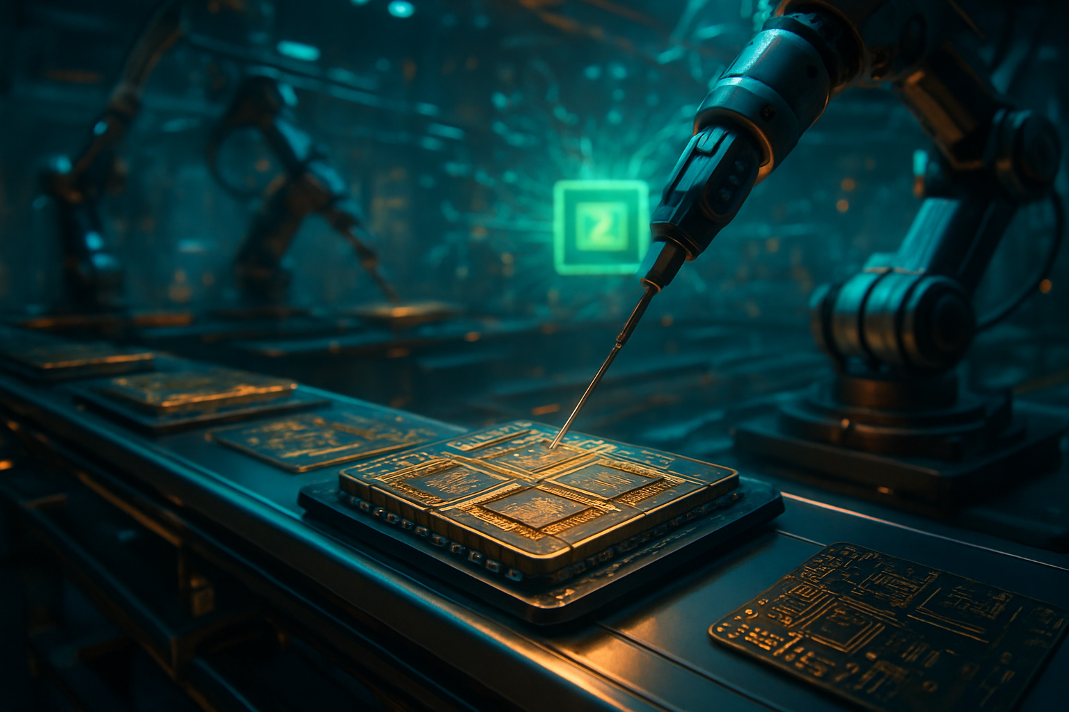
At the heart of this partnership is the Innatera Pulsar chip, the world’s first mass-market neuromorphic MCU designed specifically for "always-on" sensing at the edge. Unlike traditional processors that consume significant energy by constantly moving data between memory and the CPU, Pulsar utilizes a heterogeneous "mixed-signal" architecture that mimics the way the human brain processes information. The chip features a three-engine design: an Analog Spiking Neural Network (SNN) engine for ultra-fast signal processing, a Digital SNN engine for complex patterns, and a traditional CNN/DSP accelerator for standard AI workloads. This hardware is governed by a 160 MHz CV32E40P RISC-V CPU core, providing a familiar anchor for developers.
The technical specifications of Pulsar are a radical departure from existing technology. It delivers up to 100x lower latency and 500x lower energy consumption than conventional digital AI processors. In practical terms, this allows the chip to perform complex tasks like radar-based human presence detection at just 600 µW or audio scene classification at 400 µW—power levels so low that devices could theoretically run for years on a single coin-cell battery. The chip’s tiny 2.8 x 2.6 mm footprint makes it ideal for the burgeoning wearables market, where space and thermal management are at a premium.
Industry experts have hailed the Pulsar's release as a turning point for edge AI. While previous neuromorphic projects like Intel's (NASDAQ: INTC) Loihi were primarily restricted to research environments, Innatera has focused on commercial viability. "Innatera is a trailblazer in bringing neuromorphic computing to the real world," said Puneet Mittal, CEO and Founder of VLSI Expert. The integration of the Talamo SDK—which allows developers to port models directly from PyTorch or TensorFlow—is the "missing link" that enables engineers to utilize spiking neural networks without requiring a Ph.D. in neuroscience.
Reshaping the Semiconductor Competitive Landscape
The strategic partnership with VLSI Expert places Innatera at the center of a shifting competitive landscape. By targeting India and the United States, Innatera is tapping into the two largest pools of semiconductor design talent. In India, where the government has been aggressively pushing the "India Semiconductor Mission," the Pulsar deployment at institutions like the Silicon Institute of Technology in Bhubaneswar provides a vital bridge between academic theory and commercial silicon innovation. This talent pipeline will likely benefit major industry players such as Socionext Inc. (TYO: 6526), which is already collaborating with Innatera to integrate Pulsar with 60GHz radar sensors.
For tech giants and established chipmakers, the rise of neuromorphic MCUs represents both a challenge and an opportunity. While NVIDIA (NASDAQ: NVDA) dominates the high-power data center AI market, the "always-on" edge niche has remained largely underserved. Companies like NXP Semiconductors (NASDAQ: NXPI) and STMicroelectronics (NYSE: STM), which have long dominated the traditional MCU market, now face a disruptive force that can perform AI tasks at a fraction of the power budget. As Innatera builds a "neuromorphic-ready" workforce, these incumbents may find themselves forced to either pivot their architectures or seek aggressive partnerships to remain competitive in the wearable and IoT sectors.
Moreover, the move has significant implications for the software ecosystem. By standardizing training on RISC-V based neuromorphic hardware, Innatera and VLSI Expert are bolstering the RISC-V movement against proprietary architectures. This open-standard approach lowers the barrier to entry for startups and ODMs, such as the global lifestyle IoT device maker Joya, which are eager to integrate sophisticated AI features into low-cost consumer electronics without the licensing overhead of traditional IP.
The Broader AI Landscape: Privacy, Efficiency, and the Edge
The deployment of Pulsar chips for education reflects a broader trend in the AI landscape: the move toward "decentralized intelligence." As concerns over data privacy and the environmental cost of massive data centers grow, there is an increasing demand for devices that can process sensitive information locally and efficiently. Neuromorphic computing is uniquely suited for this, as it allows for real-time anomaly detection and gesture recognition without ever sending data to the cloud. This "privacy-by-design" aspect is a key selling point for smart home applications, such as smoke detection or elder care monitoring.
This milestone also invites comparison to the early days of the microprocessing revolution. Just as the democratization of the microprocessor in the 1970s led to the birth of the personal computer, the democratization of neuromorphic hardware could lead to an "Internet of Intelligent Things." We are moving away from the "if-this-then-that" logic of traditional sensors toward devices that can perceive and react to their environment with human-like intuition. However, the shift is not without hurdles; the industry must still establish standardized benchmarks for neuromorphic performance to help customers compare these non-traditional chips with standard DSPs.
Critics and ethicists have noted that as "always-on" sensing becomes ubiquitous and invisible, society will need to navigate new norms regarding ambient surveillance. However, proponents argue that the local-only processing nature of neuromorphic chips actually provides a more secure alternative to the current cloud-dependent AI model. By training thousands of engineers to understand these nuances today, the Innatera-VLSI Expert partnership ensures that the ethical and technical challenges of tomorrow are being addressed at the design level.
Looking Ahead: The Next Generation of Intelligent Devices
In the near term, we can expect the first wave of Pulsar-powered consumer products to hit the shelves by late 2026. These will likely include "hearables" with sub-millisecond noise cancellation and wearables capable of sophisticated vitals monitoring with unprecedented battery life. The long-term impact of the VLSI Expert partnership will be felt as the first cohort of trained designers enters the workforce, potentially leading to a surge in startups focused on niche neuromorphic applications such as predictive maintenance for industrial machinery and agricultural "smart-leaf" sensors.
Experts predict that the success of this educational rollout will serve as a blueprint for other emerging hardware sectors, such as quantum computing or photonics. As the complexity of AI hardware increases, the "supply-led" model of education—where the chipmaker provides the hardware and the tools to train the market—will likely become the standard for technological adoption. The primary challenge remains the scalability of the software stack; while the Talamo SDK is a significant step forward, further refinement will be needed to support even more complex, multi-modal spiking networks.
A New Era for Chip Design
The partnership between Innatera and VLSI Expert marks a definitive end to the era where neuromorphic computing was a "future technology." With the Pulsar chip now in the hands of students and professional developers in the US and India, brain-inspired AI has officially entered its implementation phase. This initiative does more than just sell silicon; it builds the human infrastructure required to sustain a new paradigm in computing.
As we look toward the coming months, the industry will be watching for the first "killer app" to emerge from this new generation of designers. Whether it is a revolutionary prosthetic that reacts with the speed of a human limb or a smart-city sensor that operates for a decade on a solar cell, the foundations are being laid today. The neuromorphic revolution will not be televised—it will be designed in the classrooms and laboratories of the next generation.
This content is intended for informational purposes only and represents analysis of current AI developments.
TokenRing AI delivers enterprise-grade solutions for multi-agent AI workflow orchestration, AI-powered development tools, and seamless remote collaboration platforms.
For more information, visit https://www.tokenring.ai/.