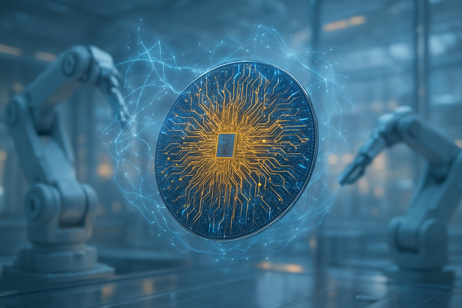
In a move that has sent shockwaves through the semiconductor industry, NVIDIA (NASDAQ:NVDA) has finalized a monumental $20 billion deal to acquire the primary assets, intellectual property, and world-class engineering talent of Groq, the pioneer of the Language Processing Unit (LPU). Announced in early January 2026, the transaction is structured as a massive "license and acqui-hire" arrangement, allowing NVIDIA to integrate Groq’s ultra-high-speed inference architecture into its own roadmap while navigating the complex regulatory landscape that has previously hampered large-scale tech mergers.
The deal represents a definitive shift in NVIDIA’s corporate strategy, signaling the end of the "Training Era" dominance and the beginning of a fierce battle for the "Inference Era." By absorbing roughly 90% of Groq’s workforce—including founder and former Google TPU architect Jonathan Ross—NVIDIA is effectively neutralizing its most potent challenger in the low-latency AI market. This $20 billion investment is aimed squarely at solving the "Memory Wall," the primary bottleneck preventing today’s AI models from achieving the instantaneous, human-like responsiveness required for next-generation agentic workflows and real-time robotics.
The Technical Leap: LPUs and the Vera Rubin Architecture
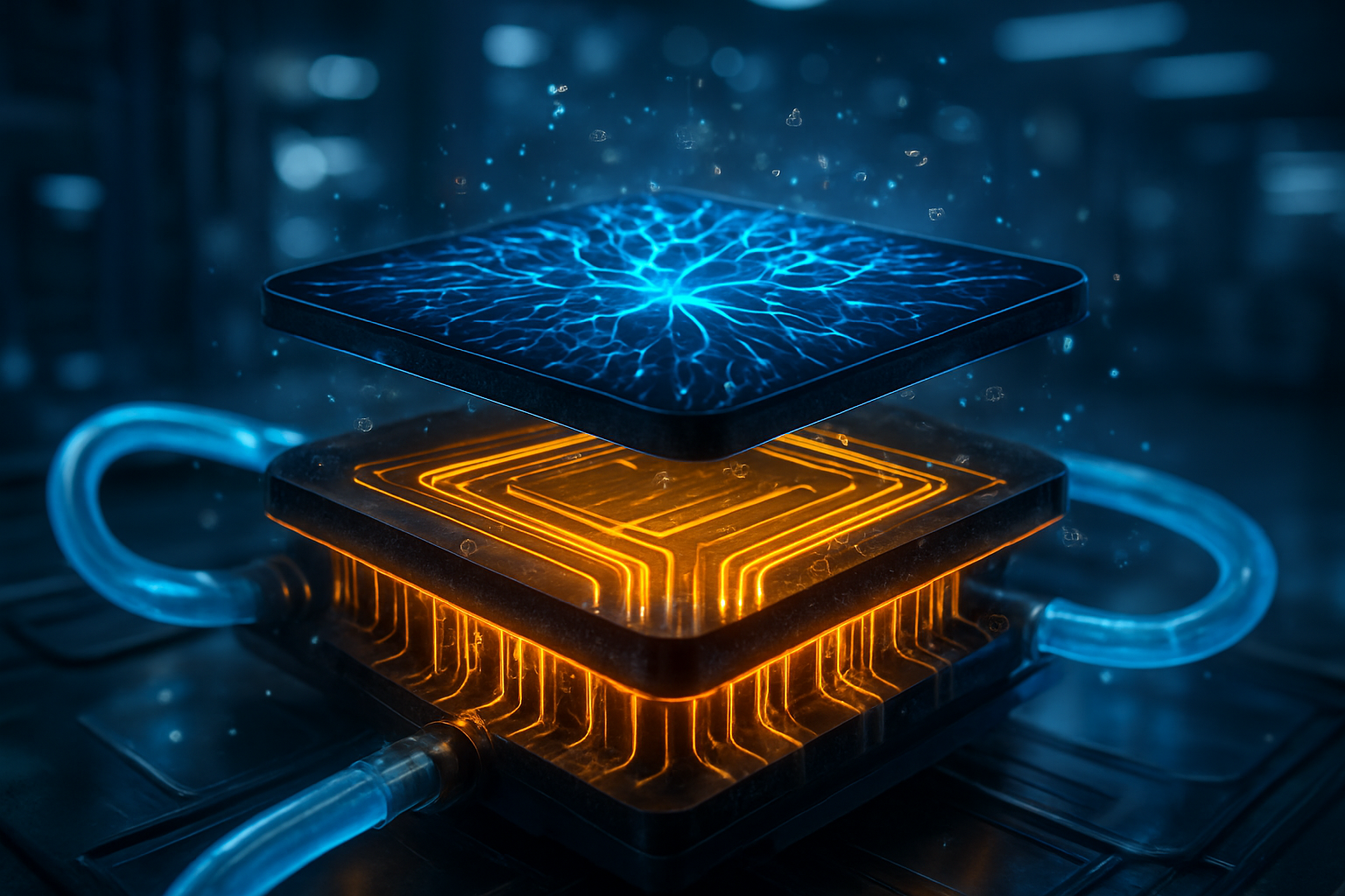
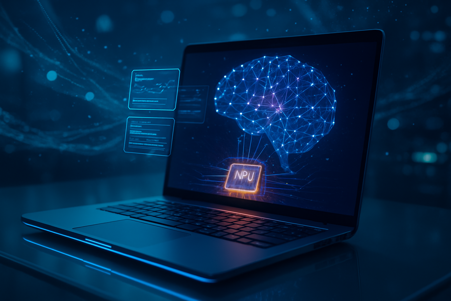
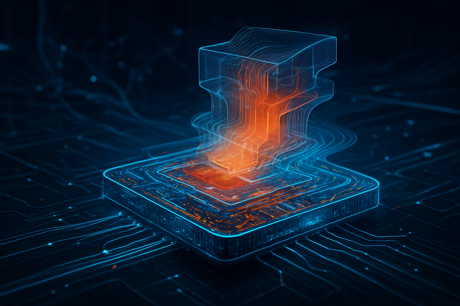
At the heart of this acquisition is Groq’s proprietary LPU technology, which differs fundamentally from NVIDIA’s traditional GPU architecture. While GPUs rely on massive parallelization and High Bandwidth Memory (HBM) to handle large batches of data, Groq’s LPU utilizes a deterministic, SRAM-based design. This architecture eliminates the need for complex memory management and allows data to move across the chip at unprecedented speeds. Technical specifications released following the deal suggest that NVIDIA is already integrating these "LPU strips" into its upcoming Vera Rubin (R100) platform. The result is the Rubin CPX (Context Processing X), a specialized module designed to handle the sequential nature of token generation with near-zero latency.
Initial performance benchmarks for the integrated Rubin-Groq hybrid chips are staggering. Engineering samples are reportedly achieving inference speeds of 500 to 800 tokens per second for large language models, a five-fold increase over the H200 series. This is achieved by keeping the active model weights in on-chip SRAM, bypassing the slow trip to external memory that plagues current-gen hardware. By combining its existing Tensor Core dominance for parallel processing with Groq’s sequential efficiency, NVIDIA has created a "heterogeneous" compute monster capable of both training the world’s largest models and serving them at the speed of thought.
The AI research community has reacted with a mix of awe and apprehension. Industry experts note that this move effectively solves the "cold start" problem for real-time AI agents. "For years, we’ve been limited by the lag in LLM responses," noted one senior researcher at OpenAI. "With Groq’s LPU logic inside the NVIDIA stack, we are moving from 'chatbots' to 'living systems' that can participate in voice-to-voice conversations without the awkward two-second pause." This technical synergy positions NVIDIA not just as a chip vendor, but as the foundational architect of the real-time AI economy.
Market Dominance and the Neutralization of Rivals
The strategic implications of this deal for the broader tech ecosystem are profound. By structuring the deal as a licensing and talent acquisition rather than a traditional merger, NVIDIA has effectively sidestepped the antitrust hurdles that famously scuttled its pursuit of Arm. While a "shell" of Groq remains as an independent cloud provider, the loss of its core engineering team and IP means it will no longer produce merchant silicon to compete with NVIDIA’s Blackwell or Rubin lines. This move effectively closes the door on a significant competitive threat just as the market for dedicated inference hardware began to explode.
For rivals like AMD (NASDAQ:AMD) and Intel (NASDAQ:INTC), the NVIDIA-Groq alliance is a daunting development. Both companies had been positioning their upcoming chips as lower-cost, high-efficiency alternatives for inference workloads. However, by incorporating Groq’s deterministic compute model, NVIDIA has undercut the primary value proposition of its competitors: specialized speed. Startups in the AI hardware space now face an even steeper uphill battle, as NVIDIA’s software ecosystem, CUDA, will now natively support LPU-accelerated workflows, making it the default choice for any developer building low-latency applications.
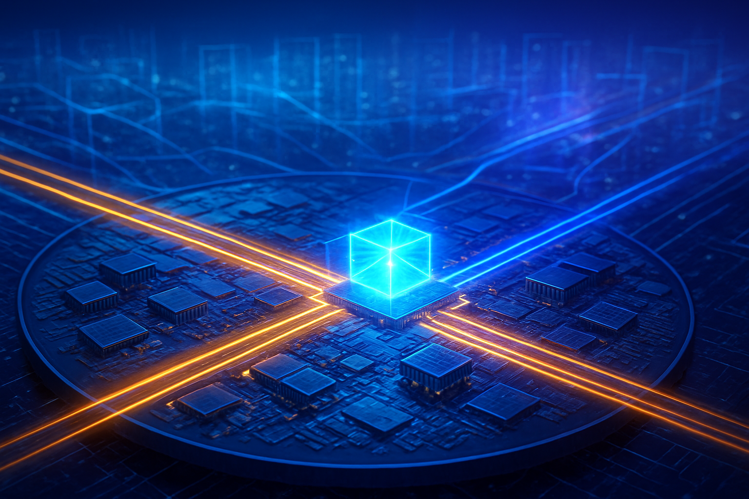
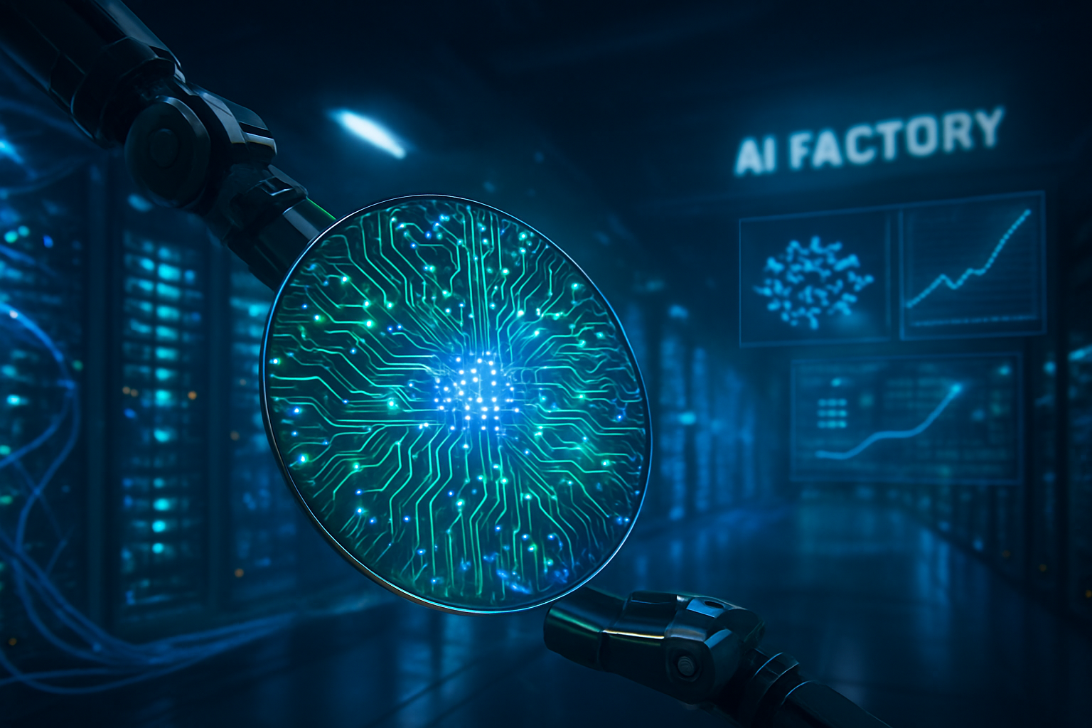
The deal also shifts the power balance among the "Hyperscalers." While Google (NASDAQ:GOOGL) and Amazon (NASDAQ:AMZN) have been developing their own in-house AI chips (TPUs and Inferentia), they now face a version of NVIDIA hardware that may outperform their custom silicon on their own cloud platforms. NVIDIA’s "AI Factory" vision is now complete; they provide the GPUs to build the model, the LPUs to run the model, and the high-speed networking to connect them. This vertical integration makes it increasingly difficult for any other player to offer a comparable price-to-performance ratio for real-time AI services.
The Broader Significance: Breaking the Memory Wall
This acquisition is more than just a corporate maneuver; it is a milestone in the evolution of computing history. Since the dawn of the modern AI boom, the industry has been constrained by the "Von Neumann bottleneck"—the delay caused by moving data between the processor and memory. Groq’s LPU architecture was the first viable solution to this problem for LLMs. By bringing this technology under the NVIDIA umbrella, the "Memory Wall" is effectively being dismantled. This marks a transition from "batch processing" AI, where efficiency comes from processing many requests at once, to "interactive AI," where efficiency comes from the speed of a single interaction.
The broader significance lies in the enablement of Agentic AI. For an AI agent to operate an autonomous vehicle or manage a complex manufacturing floor, it cannot wait for a cloud-based GPU to process a batch of data. It needs deterministic, sub-100ms response times. The integration of Groq’s technology into NVIDIA’s edge and data center products provides the infrastructure necessary for these agents to move from the lab into the real world. However, this consolidation of power also raises concerns regarding the "NVIDIA tax" and the potential for a monoculture in AI hardware that could stifle further radical innovation.
Comparisons are already being drawn to the early days of the graphics industry, where NVIDIA’s acquisition of 3dfx assets in 2000 solidified its dominance for decades. The Groq deal is viewed as the 21st-century equivalent—a strategic strike to capture the most innovative technology of a burgeoning era before it can become a standalone threat. As AI becomes the primary workload for all global compute, owning the fastest way to "think" (inference) is arguably more valuable than owning the fastest way to "learn" (training).
The Road Ahead: Robotics and Real-Time Interaction
Looking toward the near-term future, the first products featuring "Groq-infused" NVIDIA silicon are expected to hit the market by late 2026. The most immediate application will likely be in the realm of high-end enterprise assistants and real-time translation services. Imagine a global conference where every attendee wears an earpiece providing instantaneous, nuanced translation with zero perceptible lag—this is the type of use case that the Rubin CPX is designed to dominate.
In the longer term, the impact on robotics and autonomous systems will be transformative. NVIDIA’s Project GR00T, their platform for humanoid robots, will likely be the primary beneficiary of the LPU integration. For a humanoid robot to navigate a crowded room, its "brain" must process sensory input and generate motor commands in milliseconds. The deterministic nature of Groq’s architecture is perfectly suited for these safety-critical, real-time environments. Experts predict that within the next 24 months, we will see a surge in "Edge AI" deployments that were previously thought to be years away, driven by the sudden availability of ultra-low-latency compute.
However, challenges remain. Integrating two vastly different architectures—one based on parallel HBM and one on sequential SRAM—will be a monumental task for NVIDIA’s software engineers. Maintaining the ease of use that has made CUDA the industry standard while optimizing for this new hardware paradigm will be the primary focus of 2026. If successful, the result will be a unified compute platform that is virtually unassailable.
A New Era of Artificial Intelligence
The NVIDIA-Groq deal of 2026 will likely be remembered as the moment the AI industry matured from experimental research into a ubiquitous utility. By spending $20 billion to acquire the talent and technology of its fastest-moving rival, NVIDIA has not only protected its market share but has also accelerated the timeline for real-time, agentic AI. The key takeaways from this development are clear: inference is the new frontline, latency is the new benchmark, and NVIDIA remains the undisputed king of the hill.
As we move deeper into 2026, the industry will be watching closely for the first silicon benchmarks from the Vera Rubin architecture. The success of this integration will determine whether we truly enter the age of "instant AI" or if the technical hurdles of merging these two architectures prove more difficult than anticipated. For now, the message to the world is clear: NVIDIA is no longer just the company that builds the chips that train AI—it is now the company that defines how AI thinks.
This content is intended for informational purposes only and represents analysis of current AI developments.
TokenRing AI delivers enterprise-grade solutions for multi-agent AI workflow orchestration, AI-powered development tools, and seamless remote collaboration platforms.
For more information, visit https://www.tokenring.ai/.