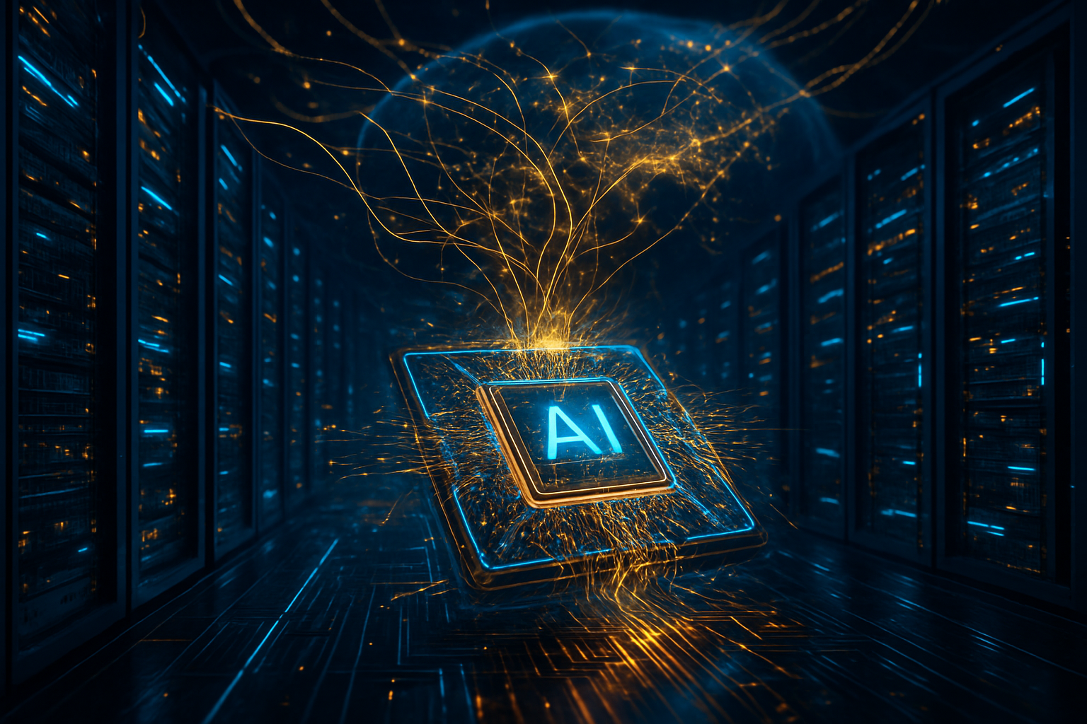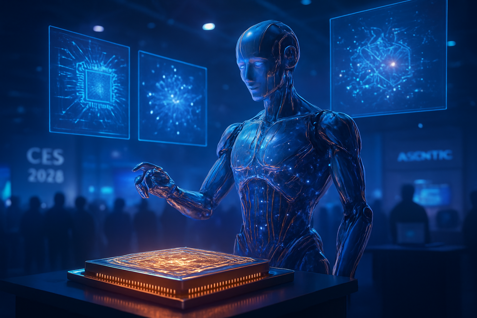
The recently concluded CES 2026 in Las Vegas will be remembered as the moment the artificial intelligence revolution stepped out of the chat box and into the physical world. Officially heralded as the "Year of Physical AI," the event marked a historic pivot from the generative text and image models of 2024–2025 toward embodied systems that can perceive, reason, and act within our three-dimensional environment. This shift was underscored by a massive coordinated push from the world’s leading semiconductor manufacturers, who unveiled a new generation of "Physical AI" processors designed to power everything from "Agentic PCs" to fully autonomous humanoid robots.
The significance of this year’s show lies in the maturation of edge computing. For the first time, the industry demonstrated that the massive compute power required for complex reasoning no longer needs to reside exclusively in the cloud. With the launch of ultra-high-performance NPUs (Neural Processing Units) from the industry's "Four Horsemen"—Nvidia, Intel, AMD, and Qualcomm—the promise of low-latency, private, and physically capable AI has finally moved from research prototypes to mass-market production.
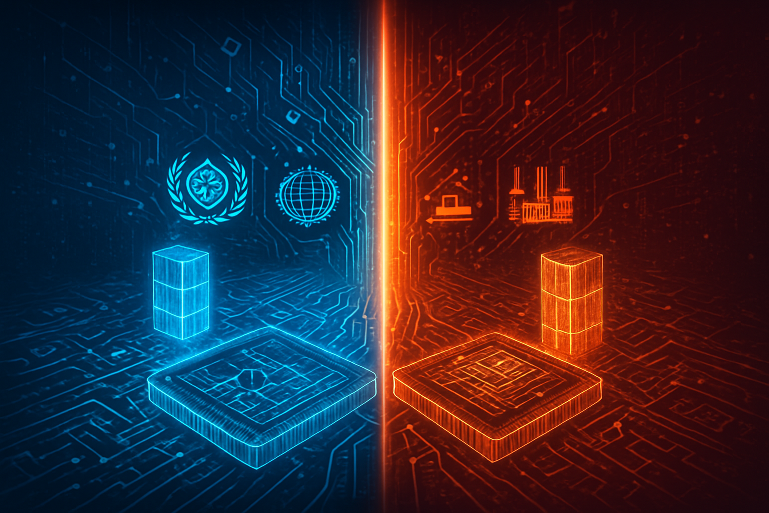
The Silicon War: Specs of the 'Four Horsemen'
The technological centerpiece of CES 2026 was the "four-way war" in AI silicon. Nvidia (NASDAQ:NVDA) set the pace early by putting its "Rubin" architecture into full production. CEO Jensen Huang declared a "ChatGPT moment for robotics" as he unveiled the Jetson T4000, a Blackwell-powered module delivering a staggering 1,200 FP4 TFLOPS. This processor is specifically designed to be the "brain" of humanoid robots, supported by Project GR00T and Cosmos, an "open world foundation model" that allows machines to learn motor tasks from video data rather than manual programming.
Not to be outdone, Intel (NASDAQ:INTC) utilized the event to showcase the success of its turnaround strategy with the official launch of Panther Lake (Core Ultra Series 3). Manufactured on the cutting-edge Intel 18A process node, the chip features the new NPU 5, which delivers 50 TOPS locally. Intel’s focus is the "Agentic AI PC"—a machine capable of managing a user’s entire digital life and local file processing autonomously. Meanwhile, Qualcomm (NASDAQ:QCOM) flexed its efficiency muscles with the Snapdragon X2 Elite Extreme, boasting an 18-core Oryon 3 CPU and an 80 TOPS NPU. Qualcomm also introduced the Dragonwing IQ10, a dedicated platform for robotics that emphasizes power-per-watt, enabling longer battery life for mobile humanoids like the Vinmotion Motion 2.
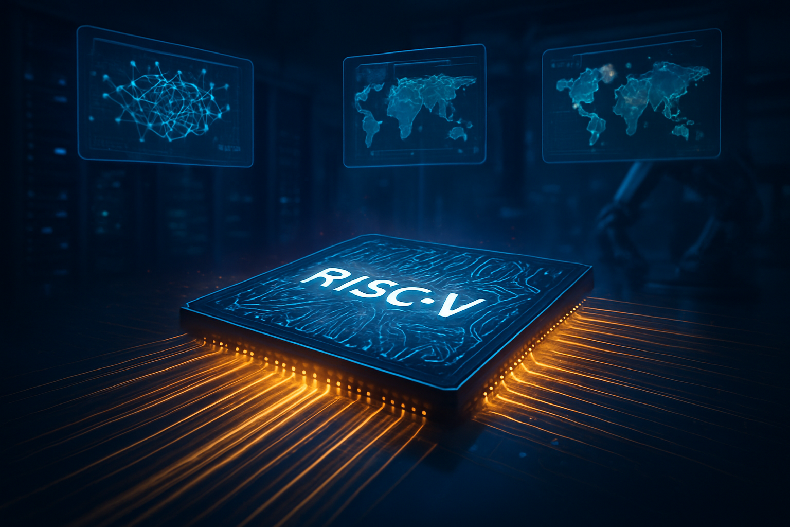
AMD (NASDAQ:AMD) rounded out the quartet by bridging the gap between the data center and the desktop. Their new Ryzen AI "Gorgon Point" series features an expanded matrix engine and the first native support for "Copilot+ Desktop" high-performance workloads. AMD also teased its Helios platform, a rack-scale solution powered by Zen 6 EPYC "Venice" processors, intended to train the very physical world models that the smaller Ryzen chips execute at the edge. Industry experts have noted that while previous years focused on software breakthroughs, 2026 is defined by the hardware's ability to handle "multimodal reasoning"—the ability for a device to see an object, understand its physical properties, and decide how to interact with it in real-time.
Market Maneuvers: From Cloud Dominance to Edge Supremacy
This shift toward Physical AI is fundamentally reshaping the competitive landscape of the tech industry. For years, the AI narrative was dominated by cloud providers and LLM developers. However, CES 2026 proved that the "edge"—the devices we carry and the robots that work alongside us—is the new battleground for strategic advantage. Nvidia is positioning itself as the "Infrastructure King," providing not just the chips but the entire software stack (Omniverse and Isaac) needed to simulate and train physical entities. By owning the simulation environment, Nvidia seeks to make its hardware the indispensable foundation for every robotics startup.
In contrast, Qualcomm and Intel are targeting the "volume market." Qualcomm is leveraging its heritage in mobile connectivity to dominate "connected robotics," where 5G and 6G integration are vital for warehouse automation and consumer bots. Intel, through its 18A manufacturing breakthrough, is attempting to reclaim the crown of the "PC Brain" by making AI features so deeply integrated into the OS that a cloud connection becomes optional. Startups like Boston Dynamics (backed by Hyundai and Google DeepMind) and Vinmotion are the primary beneficiaries of this rivalry, as the sudden abundance of high-performance, low-power silicon allows them to transition from experimental models to production-ready units capable of "human-level" dexterity.
The competitive implications extend beyond silicon. Tech giants are now forced to choose between "walled garden" AI ecosystems or open-source Physical AI frameworks. The move toward local processing also threatens the dominance of current subscription-based AI models; if a user’s Intel-powered laptop or Qualcomm-powered robot can perform complex reasoning locally, the strategic advantage of centralized AI labs like OpenAI or Anthropic could begin to erode in favor of hardware-software integrated giants.
The Wider Significance: When AI Gets a Body
The transition from "Digital AI" to "Physical AI" represents a profound milestone in human-computer interaction. For the first time, the "hallucinations" that plagued early generative AI have moved from being a nuisance in text to a safety critical engineering challenge. At CES 2026, panels featuring leaders from Siemens and Mercedes-Benz emphasized that "Physical AI" requires "error intolerance." A robot navigating a crowded home or a factory floor cannot afford a single reasoning error, leading to the introduction of "safety-grade" silicon architectures that partition AI logic from critical motor controls.
This development also brings significant societal concerns to the forefront. As AI becomes embedded in physical infrastructure—from elevators that predict maintenance to autonomous industrial helpers—the question of accountability becomes paramount. Experts at the event raised alarms regarding "invisible AI," where autonomous systems become so pervasive that their decision-making processes are no longer transparent to the humans they serve. The industry is currently racing to establish "document trails" for AI reasoning to ensure that when a physical system fails, the cause can be diagnosed with the same precision as a mechanical failure.
Comparatively, the 2023 generative AI boom was about "creation," while the 2026 Physical AI breakthrough is about "utility." We are moving away from AI as a toy or a creative partner and toward AI as a functional laborer. This has reignited debates over labor displacement, but with a new twist: the focus is no longer just on white-collar "knowledge work," but on blue-collar tasks in logistics, manufacturing, and elder care.
Beyond the Horizon: The 2027 Roadmap
Looking ahead, the momentum generated at CES 2026 shows no signs of slowing. Near-term developments will likely focus on the refinement of "Agentic AI PCs," where the operating system itself becomes a proactive assistant that performs tasks across different applications without user prompting. Long-term, the industry is already looking toward 2027, with Intel teasing its Nova Lake architecture (rumored to feature 52 cores) and AMD preparing its Medusa (Zen 6) chips based on TSMC’s 2nm process. These upcoming iterations aim to bring even more "brain-like" density to consumer hardware.
The next major challenge for the industry will be the "sim-to-real" gap—the difficulty of taking an AI trained in a virtual simulation and making it function perfectly in the messy, unpredictable real world. Future applications on the horizon include "personalized robotics," where robots are not just general-purpose tools but are fine-tuned to the specific layout and needs of an individual's home. Predictably, experts believe the next 18 months will see a surge in M&A activity as silicon giants move to acquire robotics software startups to complete their "Physical AI" portfolios.
The Wrap-Up: A Turning Point in Computing History
CES 2026 has served as a definitive declaration that the "post-chat" era of artificial intelligence has arrived. The key takeaways from the event are clear: the hardware has finally caught up to the software, and the focus of innovation has shifted from virtual outputs to physical actions. The coordinated launches from Nvidia, Intel, AMD, and Qualcomm have provided the foundation for a world where AI is no longer a guest on our screens but a participant in our physical spaces.
In the history of AI, 2026 will likely be viewed as the year the technology gained its "body." As we look toward the coming months, the industry will be watching closely to see how these new processors perform in real-world deployments and how consumers react to the first wave of truly autonomous "Agentic" devices. The silicon war is far from over, but the battlefield has officially moved into the real world.
This content is intended for informational purposes only and represents analysis of current AI developments.
TokenRing AI delivers enterprise-grade solutions for multi-agent AI workflow orchestration, AI-powered development tools, and seamless remote collaboration platforms.
For more information, visit https://www.tokenring.ai/.