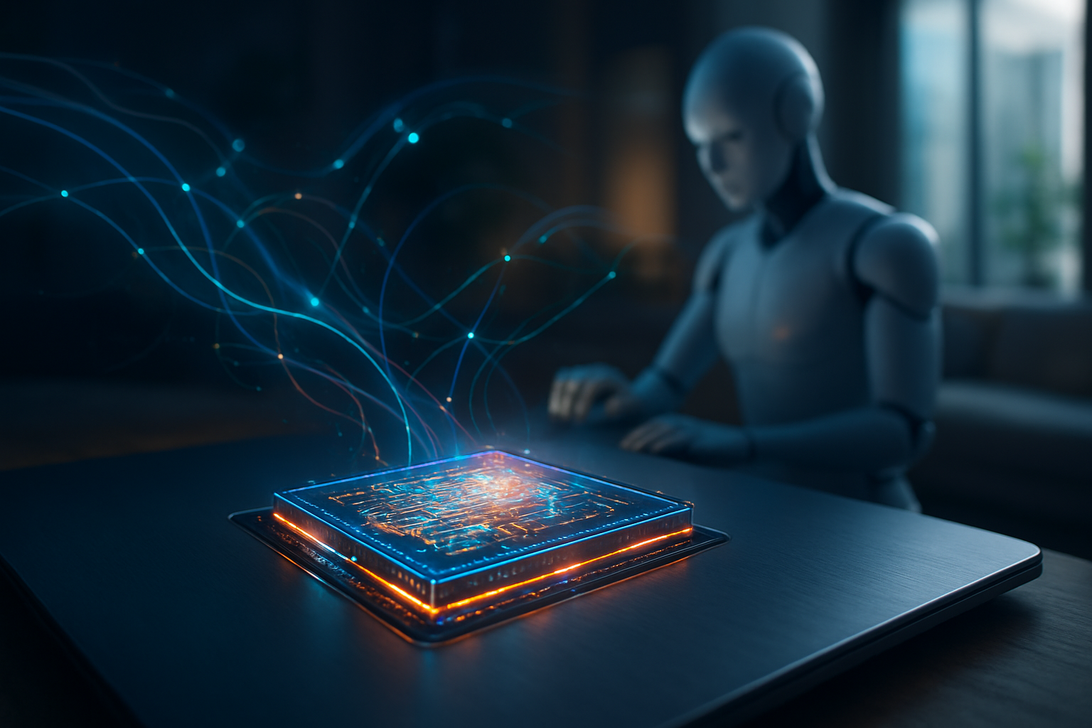
The dust has settled on CES 2026, and the verdict from the tech industry is unanimous: we have officially entered the Year of Physical AI. For the past three years, artificial intelligence was largely a "cloud-first" phenomenon—a digital brain trapped in a data center, accessible only via an internet connection. However, the announcements in Las Vegas this month have signaled a tectonic shift. AI has finally moved from the server rack to the "edge," manifesting in hardware that can perceive, reason about, and interact with the physical world in real-time, without a single byte leaving the local device.
This "Edge AI Revolution" is powered by a new generation of silicon that has turned the personal computer into an "AI Hub." With the release of groundbreaking hardware from industry titans like Intel (NASDAQ:INTC) and Qualcomm (NASDAQ:QCOM), the 2026 hardware landscape is defined by its ability to run complex, multi-modal local agents. These are not mere chatbots; they are proactive systems capable of managing entire digital and physical workflows. The era of "AI-as-a-service" is being challenged by "AI-as-an-appliance," bringing unprecedented privacy, speed, and autonomy to the average consumer.
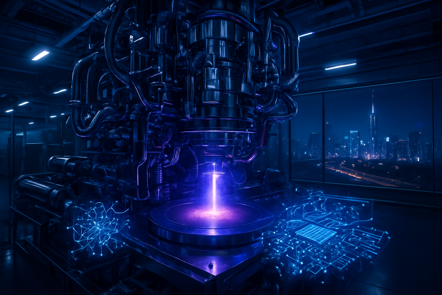
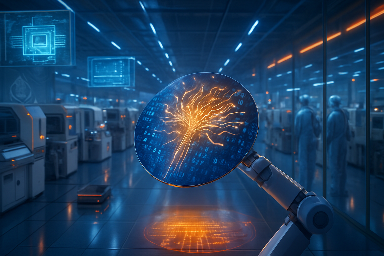
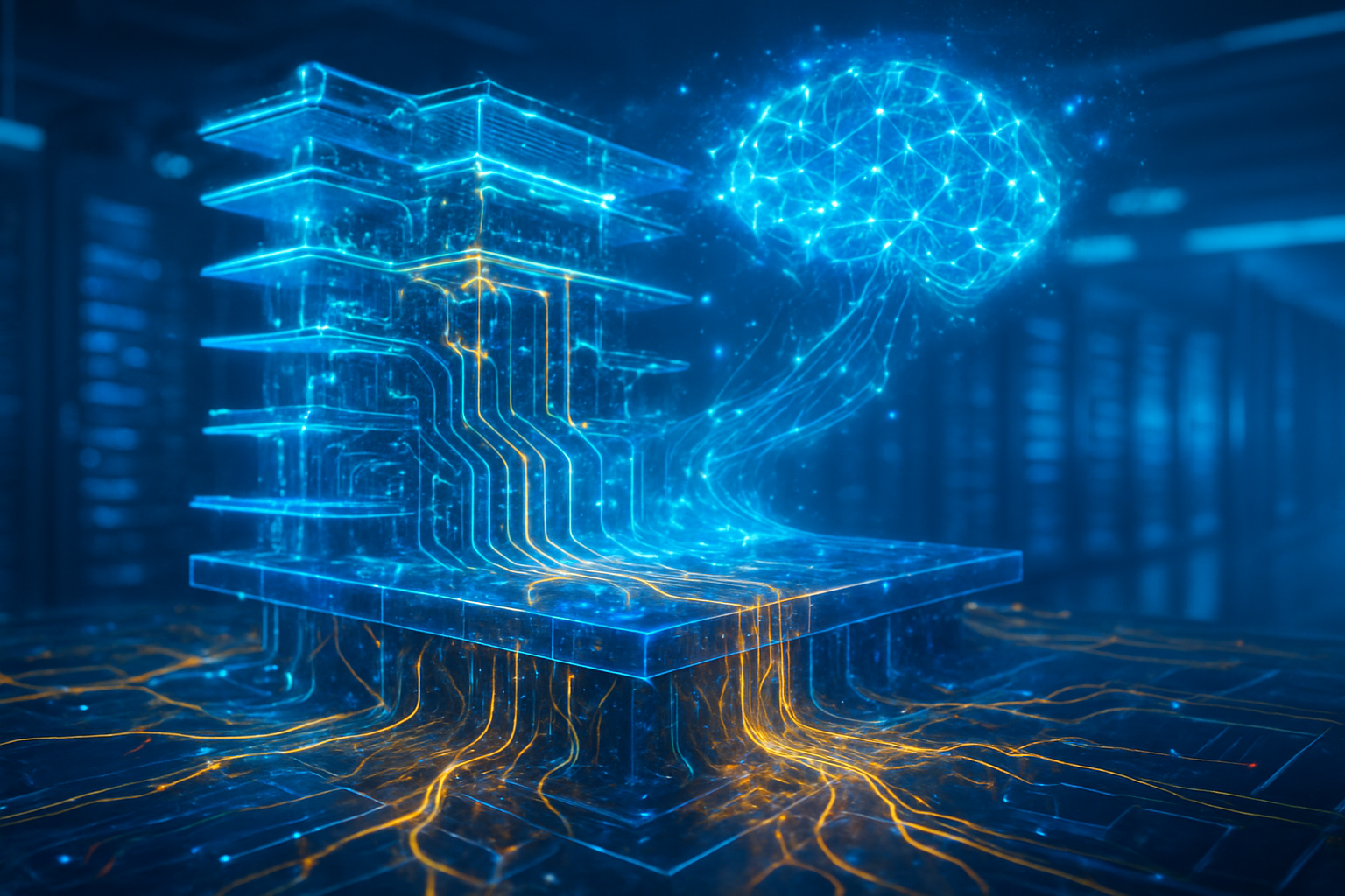
The 100 TOPS Milestone: Under the Hood of the 2026 AI PC
The technical narrative of 2026 is dominated by the race for Neural Processing Unit (NPU) supremacy. At the heart of this transition is Intel’s Panther Lake (Core Ultra Series 3), which officially launched at CES 2026. Built on the cutting-edge Intel 18A process, Panther Lake features the new NPU 5 architecture, delivering a dedicated 50 TOPS (Tera Operations Per Second). When paired with the integrated Arc Xe3 "Celestial" graphics, the total platform performance reaches a staggering 170 TOPS. This allows laptops to perform complex video editing and local 3D rendering that previously required a dedicated desktop GPU.
Not to be outdone, Qualcomm (NASDAQ:QCOM) showcased the Snapdragon X2 Elite Extreme, specifically designed for the next generation of Windows on Arm. Its Hexagon NPU 6 achieves a massive 85 TOPS, setting a new benchmark for dedicated NPU performance in ultra-portable devices. Even more impressive was the announcement of the Snapdragon 8 Elite Gen 5 for mobile devices, which became the first mobile chipset to hit the 100 TOPS NPU milestone. This level of local compute power allows "Small Language Models" (SLMs) to run at speeds exceeding 200 tokens per second, enabling real-time, zero-latency voice and visual interaction.
This represents a fundamental departure from the 2024 era of AI PCs. While early devices like those powered by the original Lunar Lake or Snapdragon X Elite could handle basic background blurring and text summarization, the 2026 class of hardware can host "Agentic AI." These systems utilize local "world models"—AI that understands physical constraints and cause-and-effect—allowing them to control robotics or manage complex multi-app tasks locally. Industry experts note that the 100 TOPS threshold is the "magic number" required for AI to move from passive response to active agency.
The Battle for the Edge: Market Implications and Strategic Shifts
The shift toward edge-based Physical AI has created a high-stakes battleground for silicon supremacy. Intel (NASDAQ:INTC) is leveraging its 18A manufacturing process to prove it can out-innovate competitors in both design and fabrication. By hitting the 50 TOPS NPU floor across its entire consumer line, Intel is forcing a rapid obsolescence of non-AI hardware, effectively mandating a global PC refresh cycle. Meanwhile, Qualcomm (NASDAQ:QCOM) is tightening its grip on the high-efficiency laptop market, challenging Apple (NASDAQ:AAPL) for the title of best performance-per-watt in the mobile computing space.
This revolution also poses a strategic threat to traditional cloud providers like Alphabet (NASDAQ:GOOGL) and Amazon (NASDAQ:AMZN). As more AI processing moves to the device, the reliance on expensive cloud inference is diminishing for standard tasks. Microsoft (NASDAQ:MSFT) has recognized this shift by launching the "Agent Hub" for Windows, an OS-level orchestration layer that allows local agents to coordinate tasks. This move ensures that even as AI becomes local, Microsoft remains the dominant platform for its execution.
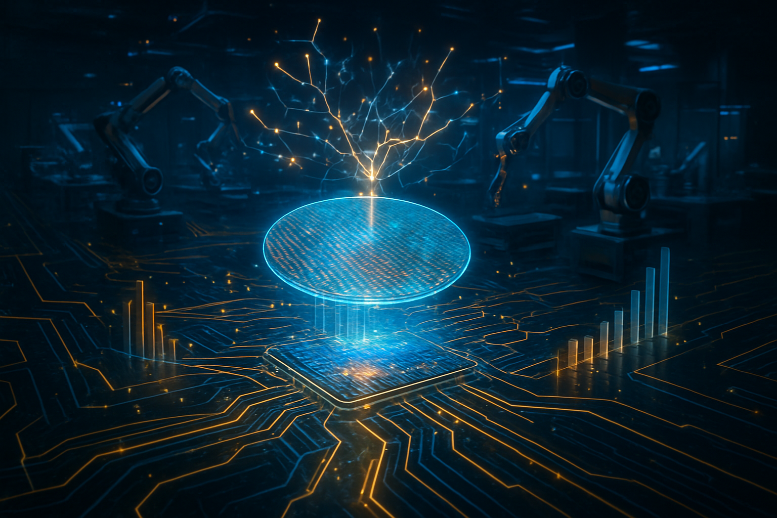
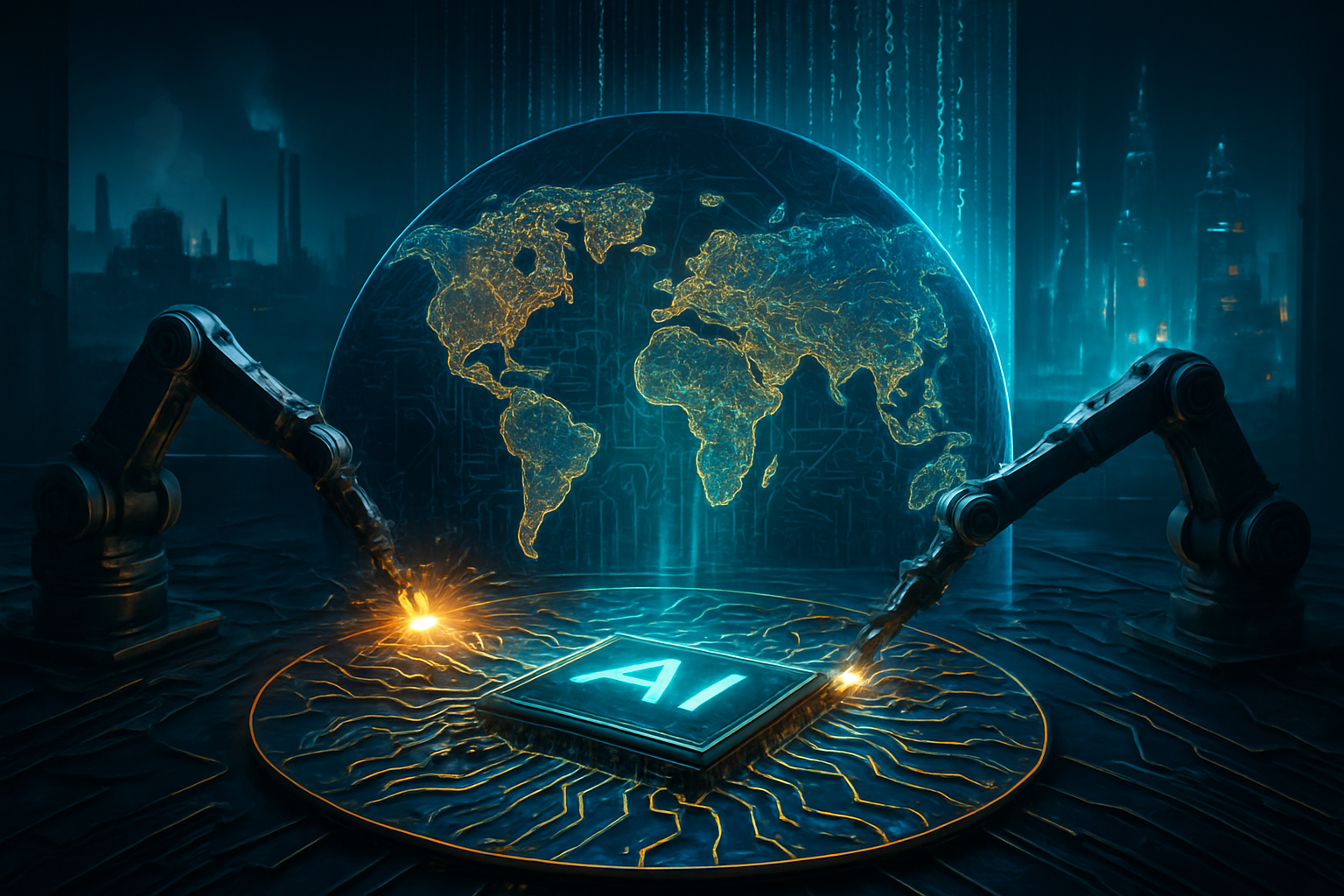
The robotics sector is perhaps the biggest beneficiary of this edge computing surge. At CES 2026, NVIDIA (NASDAQ:NVDA) solidified its lead in Physical AI with the Vera Rubin architecture and the Cosmos reasoning model. By providing the "brains" for companies like LG (KRX:066570) and Hyundai (OTC:HYMTF), NVIDIA is positioning itself as the foundational layer of the robotics economy. The market is shifting from "software-only" AI startups to those that can integrate AI into physical hardware, marking a return to tangible, product-based innovation.
Beyond the Screen: Privacy, Latency, and the Physical AI Landscape
The emergence of "Physical AI" addresses the two greatest hurdles of the previous AI era: privacy and latency. In 2026, the demand for Sovereign AI—the ability for individuals and corporations to own and control their data—has hit an all-time high. Local execution on NPUs means that sensitive data, such as a user’s calendar, private messages, and health data, never needs to be uploaded to a third-party server. This has opened the door for highly personalized agents like Lenovo’s (HKG:0992) "Qira," which indexes a user’s entire digital life locally to provide proactive assistance without compromising privacy.
The latency improvements of 2026 hardware are equally transformative. For Physical AI—such as LG’s CLOiD home robot or the electric Atlas from Boston Dynamics—sub-millisecond reaction times are a necessity, not a luxury. By processing sensory input locally, these machines can navigate complex environments and interact with humans safely. This is a significant milestone compared to early cloud-dependent robots that were often hampered by "thinking" delays.
However, this rapid advancement is not without its concerns. The "Year of Physical AI" brings new challenges regarding the safety and ethics of autonomous physical agents. If a local AI agent can independently book travel, manage bank accounts, or operate heavy machinery in a home or factory, the potential for hardware-level vulnerabilities becomes a physical security risk. Governments and regulatory bodies are already pivoting their focus from "content moderation" to "robotic safety standards," reflecting the shift from digital to physical AI impacts.
The Horizon: From AI PCs to Zero-Labor Environments
Looking beyond 2026, the trajectory of Edge AI points toward "Zero-Labor" environments. Intel has already teased its Nova Lake architecture for 2027, which is expected to be the first x86 chip to reach 100 TOPS on the NPU alone. This will likely make sophisticated local AI agents a standard feature even in budget-friendly hardware. We are also seeing the early stages of a unified "Agentic Ecosystem," where your smartphone, PC, and home robots share a local intelligence mesh, allowing them to pass tasks between one another seamlessly.
Future applications currently on the horizon include "Ambient Computing," where the AI is no longer something you interact with through a screen, but a layer of intelligence that exists in the environment itself. Experts predict that by 2028, the concept of a "Personal AI Agent" will be as ubiquitous as the smartphone is today. These agents will be capable of complex reasoning, such as negotiating bills on your behalf or managing home energy systems to optimize for both cost and carbon footprint, all while running on local, renewable-powered edge silicon.
A New Chapter in the History of Computing
The "Year of Physical AI" will be remembered as the moment AI became truly useful for the average person. It is the year we moved past the novelty of generative text and into the utility of agentic action. The Edge AI revolution, spearheaded by the incredible engineering of 2026 silicon, has decentralized intelligence, moving it out of the hands of a few cloud giants and back onto the devices we carry and the machines we live with.
The key takeaway from CES 2026 is that the hardware has finally caught up to the software's ambition. As we look toward the rest of the year, watch for the rollout of "Agentic" OS updates and the first true commercial deployment of household humanoid assistants. The "Silicon Soul" has arrived, and it lives locally.
This content is intended for informational purposes only and represents analysis of current AI developments.
TokenRing AI delivers enterprise-grade solutions for multi-agent AI workflow orchestration, AI-powered development tools, and seamless remote collaboration platforms.
For more information, visit https://www.tokenring.ai/.