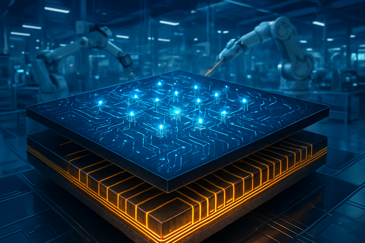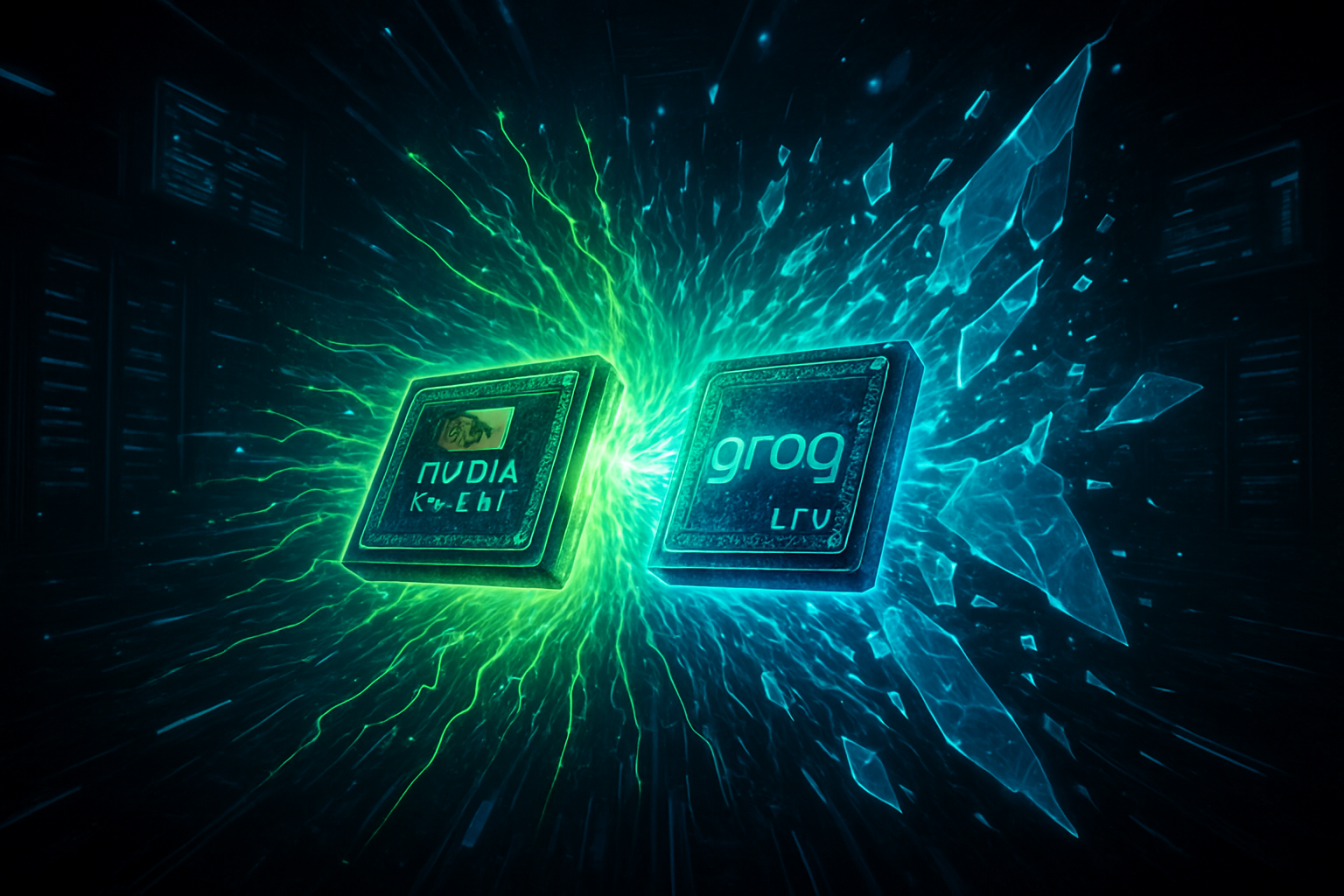
In a move that has sent shockwaves through Silicon Valley and global financial markets, NVIDIA (NASDAQ: NVDA) has officially finalized a landmark $20 billion strategic licensing and "acqui-hire" deal with Groq, the pioneer of the Language Processing Unit (LPU). Announced in late December 2025 and moving into full integration phase as of January 2026, the deal represents NVIDIA’s most aggressive maneuver to date to consolidate its lead in the burgeoning "Inference Economy." By absorbing Groq’s core intellectual property and its world-class engineering team—including legendary founder Jonathan Ross—NVIDIA aims to fuse Groq’s ultra-high-speed deterministic compute with its upcoming "Rubin" architecture, scheduled for a late 2026 release.
The significance of this deal cannot be overstated; it marks a fundamental shift in NVIDIA's architectural philosophy. While NVIDIA has dominated the AI training market for a decade, the industry is rapidly pivoting toward high-volume inference, where speed and latency are the only metrics that matter. By integrating Groq’s specialized LPU technology, NVIDIA is positioning itself to solve the "memory wall"—the physical limitation where data transfer speeds between memory and processors cannot keep up with the demands of massive Large Language Models (LLMs). This acquisition signals the end of the era of general-purpose AI hardware and the beginning of a specialized, inference-first future.
Breaking the Memory Wall: LPU Tech Meets the Rubin Platform
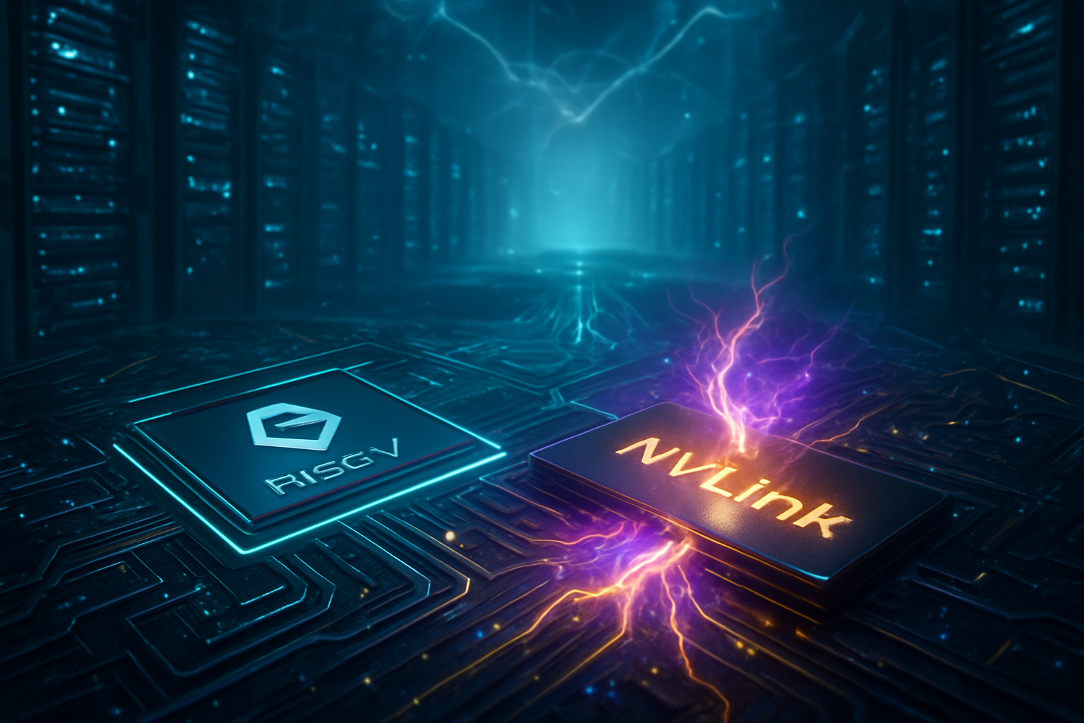
The technical centerpiece of this $20 billion deal is the integration of Groq’s SRAM-based (Static Random Access Memory) architecture into NVIDIA’s Rubin platform. Unlike traditional GPUs that rely on High Bandwidth Memory (HBM), which resides off-chip and introduces significant latency penalties, Groq’s LPU utilizes a "software-defined hardware" approach. By placing memory directly on the chip and using a proprietary compiler to pre-schedule every data movement down to the nanosecond, Groq’s tech achieves deterministic performance. In early benchmarks, Groq systems have demonstrated the ability to run models like Llama 3 at speeds exceeding 400 tokens per second—roughly ten times faster than current-generation hardware.
The Rubin platform, which succeeds the Blackwell architecture, will now feature a hybrid memory hierarchy. While Rubin will still utilize HBM4 for massive model parameters, it is expected to incorporate a "Groq-layer" of high-speed SRAM inference cores. This combination allows the system to overcome the "memory wall" by keeping the most critical, frequently accessed data in the ultra-fast SRAM buffer, while the broader model sits in HBM4. This architectural synergy is designed to support the next generation of "Agentic AI"—autonomous systems that require near-instantaneous reasoning and multi-step planning to function in real-time environments.
Industry experts have reacted with a mix of awe and concern. Dr. Sarah Chen, lead hardware analyst at SemiAnalysis, noted that "NVIDIA essentially just bought the only viable threat to its inference dominance." The AI research community is particularly excited about the deterministic nature of the Groq-Rubin integration. Unlike current GPUs, which suffer from performance "jitter" due to complex hardware scheduling, the new architecture provides a guaranteed, constant latency. This is a prerequisite for safety-critical AI applications in robotics, autonomous vehicles, and high-frequency financial modeling.
Strategic Dominance and the 'Acqui-Hire' Model
This deal is a masterstroke of corporate strategy and regulatory maneuvering. By structuring the agreement as a $20 billion licensing deal combined with a mass talent migration—rather than a traditional acquisition—NVIDIA appears to have circumvented the protracted antitrust scrutiny that famously derailed its attempt to buy ARM in 2022. The deal effectively brings Groq’s 300+ engineers into the NVIDIA fold, with Jonathan Ross, a principal architect of the original Google TPU at Alphabet (NASDAQ: GOOGL), now serving as a Senior Vice President of Inference Architecture at NVIDIA.
For competitors like Advanced Micro Devices (NASDAQ: AMD) and Intel (NASDAQ: INTC), the NVIDIA-Groq alliance creates a formidable barrier to entry. AMD has made significant strides with its MI300 and MI400 series, but it remains heavily reliant on HBM-based architectures. By pivoting toward the Groq-style SRAM model for inference, NVIDIA is diversifying its technological portfolio in a way that its rivals may struggle to replicate without similar multi-billion-dollar investments. Startups in the AI chip space, such as Cerebras and SambaNova, now face a landscape where the market leader has just absorbed their most potent architectural rival.
The market implications extend beyond just hardware sales. By controlling the most efficient inference platform, NVIDIA is also solidifying its software moat. The integration of GroqWare—Groq's highly optimized compiler stack—into NVIDIA’s CUDA ecosystem means that developers will be able to deploy ultra-low-latency models without learning an entirely new programming language. This vertical integration ensures that NVIDIA remains the default choice for the world’s largest hyperscalers and cloud service providers, who are desperate to lower the cost-per-token of running AI services.
A New Era of Real-Time, Agentic AI
The broader significance of the NVIDIA-Groq deal lies in its potential to unlock "Agentic AI." Until now, AI has largely been a reactive tool—users prompt, and the model responds with a slight delay. However, the future of the industry revolves around agents that can think, plan, and act autonomously. These agents require "Fast Thinking" capabilities that current GPU architectures struggle to provide at scale. By incorporating LPU technology, NVIDIA is providing the "nervous system" required for AI that operates at the speed of human thought, or faster.
This development also aligns with the growing trend of "Sovereign AI." Many nations are now building their own domestic AI infrastructure to ensure data privacy and national security. Groq had already established a strong foothold in this sector, recently securing a $1.5 billion contract for a data center in Saudi Arabia. By acquiring this expertise, NVIDIA is better positioned to partner with governments around the world, providing turnkey solutions that combine high-performance compute with the specific architectural requirements of sovereign data centers.
However, the consolidation of such massive power in one company's hands remains a point of concern for the industry. Critics argue that NVIDIA’s "virtual buyout" of Groq further centralizes the AI supply chain, potentially leading to higher prices for developers and limited architectural diversity. Comparison to previous milestones, like the acquisition of Mellanox, suggests that NVIDIA will use this deal to tighten the integration of its networking and compute stacks, making it increasingly difficult for customers to "mix and match" components from different vendors.
The Road to Rubin and Beyond
Looking ahead, the next 18 months will be a period of intense integration. The immediate focus is on merging Groq’s compiler technology with NVIDIA’s TensorRT-LLM software. The first hardware fruit of this labor will likely be the R100 "Rubin" GPU. Sources close to the project suggest that NVIDIA is also exploring the possibility of "mini-LPUs"—specialized inference blocks that could be integrated into consumer-grade hardware, such as the rumored RTX 60-series, enabling near-instant local LLM processing on personal workstations.
Predicting the long-term impact, many analysts believe this deal marks the beginning of the "post-GPU" era for AI. While the term "GPU" will likely persist as a brand, the internal architecture is evolving into a heterogeneous "AI System on a Chip." Challenges remain, particularly in scaling SRAM to the levels required for the trillion-parameter models of 2027 and beyond. Nevertheless, the industry expects that by the time the Rubin platform ships in late 2026, it will set a new world record for inference efficiency, potentially reducing the energy cost of AI queries by an order of magnitude.
Conclusion: Jensen Huang’s Final Piece of the Puzzle
The $20 billion NVIDIA-Groq deal is more than just a transaction; it is a declaration of intent. By bringing Jonathan Ross and his LPU technology into the fold, Jensen Huang has successfully addressed the one area where NVIDIA was perceived as potentially vulnerable: ultra-low-latency inference. The "memory wall," which has long been the Achilles' heel of high-performance computing, is finally being dismantled through a combination of SRAM-first design and deterministic software control.
As we move through 2026, the tech world will be watching closely to see how quickly the Groq team can influence the Rubin roadmap. If successful, this integration will cement NVIDIA’s status not just as a chipmaker, but as the foundational architect of the entire AI era. For now, the "Inference Economy" has a clear leader, and the gap between NVIDIA and the rest of the field has never looked wider.
This content is intended for informational purposes only and represents analysis of current AI developments.
TokenRing AI delivers enterprise-grade solutions for multi-agent AI workflow orchestration, AI-powered development tools, and seamless remote collaboration platforms.
For more information, visit https://www.tokenring.ai/.