As of January 19, 2026, the global semiconductor industry stands on the precipice of a historic milestone. Once a cyclical sector defined by the ebbs and flows of consumer electronics, the chip market has transformed into a secular powerhouse. Recent projections from BofA Securities and leading consulting firms like McKinsey & Company indicate that the global chip market is no longer merely "on track" to reach $1 trillion by 2030—it is likely to cross that threshold as early as late 2026 or 2027. This acceleration, driven by an insatiable demand for Generative AI infrastructure and a fundamental architecture shift in the automotive and industrial sectors, marks the beginning of what many are calling the "Semiconductor Decade."
The immediate significance of this growth cannot be overstated. In 2023, the industry generated roughly $527 billion in revenue. By the end of 2025, that figure had surged to approximately $793 billion. This meteoric rise is underpinned by the transition from general-purpose computing to "accelerated computing," where specialized silicon is required to handle the massive datasets of the AI era. As the world moves toward sovereign AI clouds and autonomous physical systems, the semiconductor has solidified its status as the "new oil," a critical resource for national security and economic dominance.
The Technical Vanguard: Rubin, HBM4, and the 2nm Leap
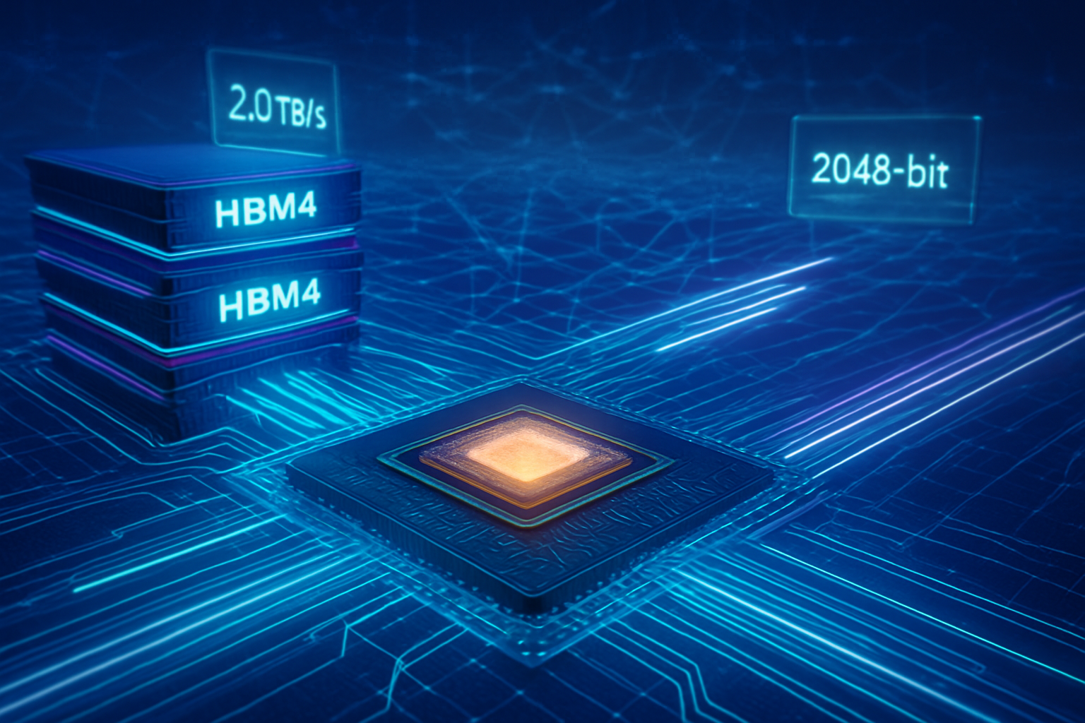
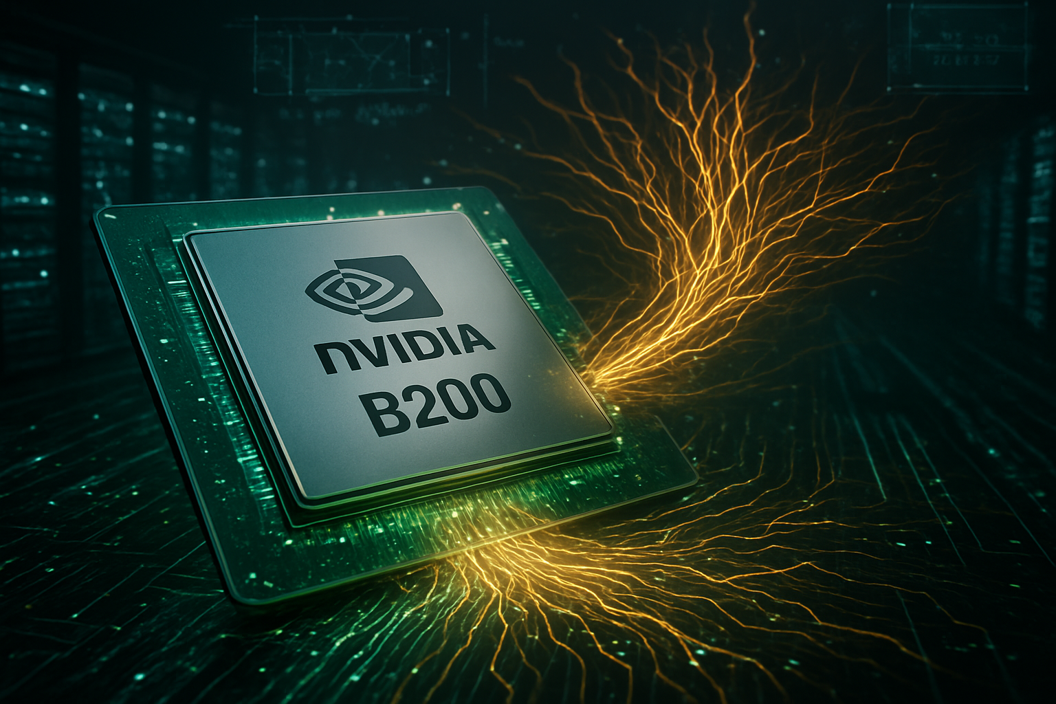
The push toward the $1 trillion mark is being fueled by a series of unprecedented technical breakthroughs. At the forefront is the launch of the Nvidia (NASDAQ: NVDA) Rubin platform, which officially succeeded the Blackwell architecture at the start of 2026. The Rubin R100 GPU represents a paradigm shift, delivering an estimated 50 Petaflops of FP4 compute performance. This is achieved through the first-ever exclusive use of High Bandwidth Memory 4 (HBM4). Unlike its predecessors, HBM4 doubles the interface width to 2048-bit, effectively shattering the "memory wall" that has long throttled AI training speeds.
Manufacturing has also entered the "Angstrom Era." TSMC (NYSE: TSM) has successfully reached high-volume manufacturing for its 2nm (N2) node, utilizing Nanosheet Gate-All-Around (GAA) transistors for the first time. Simultaneously, Intel (NASDAQ: INTC) has reported stable yields for its 18A (1.8nm) process, marking a successful deployment of RibbonFET and PowerVia backside power delivery. These technologies allow for higher transistor density and significantly improved energy efficiency—a prerequisite for the next generation of data centers that are already straining global power grids.
Furthermore, the "Power Revolution" in automotive and industrial IoT is being led by Wide-Bandgap (WBG) materials. Silicon Carbide (SiC) has transitioned to 200mm (8-inch) wafers, enabling 800V architectures to become the standard for electric vehicles (EVs). These chips provide a 7% range improvement over traditional silicon, a critical factor for the mass adoption of EVs. In the industrial space, Infineon (OTC: IFNNY) has pioneered 300mm Gallium Nitride (GaN) production, which has unlocked 30% efficiency gains for AI-driven smart factories and renewable energy grids.
Market Dominance and the Battle for Silicon Supremacy
The shift toward a $1 trillion market is reshuffling the corporate leaderboard. Nvidia has solidified its position as the world’s largest semiconductor company by revenue, surpassing legacy giants Samsung (KRX: 005930) and Intel. However, the ecosystem’s growth is benefiting a broad spectrum of players. Broadcom (NASDAQ: AVGO) has seen its networking and custom ASIC business skyrocket as hyperscalers like Meta and Google seek to build proprietary AI accelerators to reduce their reliance on off-the-shelf components.
The competitive landscape is also being defined by the "Foundry War" between TSMC, Intel, and Samsung. TSMC remains the dominant player, securing nearly all of the world’s 2nm capacity for 2026, while Intel’s 18A node has successfully attracted high-profile foundry customers like Microsoft (NASDAQ: MSFT) and Amazon (NASDAQ: AMZN). This diversification of the manufacturing base is seen as a strategic advantage for the U.S. and Europe, which have leveraged the CHIPS Act to incentivize domestic production and insulate the supply chain from geopolitical volatility.
Startups and mid-sized firms are also finding niches in the "Edge AI" and RISC-V sectors. As companies like Qualcomm (NASDAQ: QCOM) and AMD (NASDAQ: AMD) push AI capabilities directly into smartphones and PCs, the demand for low-power, highly customized silicon has surged. RISC-V, an open-standard instruction set architecture, has reached a 25% market share in specialized segments, allowing manufacturers to bypass expensive licensing fees and design chips tailored for specific AI agentic workflows.
Geopolitics, Sovereignty, and the AI Landscape
The broader significance of the trillion-dollar chip market lies in its intersection with global politics and sustainability. We have entered the era of "Sovereign AI," where nations are treating semiconductor capacity as a pillar of national identity. Countries across the Middle East, Europe, and Asia are investing billions to build localized data centers and domestic chip design capabilities. This trend is a departure from the globalized efficiency of the 2010s, favoring resiliency and self-reliance over lowest-cost production.
However, this rapid expansion has raised significant concerns regarding environmental impact. The energy consumption of AI data centers is projected to double by 2030. This has placed immense pressure on chipmakers to innovate in "green silicon"—chips that provide more compute-per-watt. The transition to GaN and SiC is part of this solution, but experts warn that the sheer scale of the $1 trillion market will require even more radical breakthroughs in photonic computing and 3D chip stacking to keep emissions in check.
Comparatively, the current AI milestone exceeds the "Internet Boom" of the late 90s in both scale and speed. While the internet era was defined by connectivity, the AI era is defined by autonomy. The chips being produced in 2026 are not just processors; they are the "brains" for autonomous robots, software-defined vehicles, and real-time industrial optimizers. This shift from passive tools to active agents marks a fundamental change in how technology integrates with human society.
Looking Ahead: The 1.4nm Frontier and Humanoid Robotics
As we look toward the 2027–2030 window, the roadmap is already being drawn. The next great challenge will be the move to 1.4nm (A14) nodes, which will require the full-scale deployment of High-NA EUV lithography machines from ASML (NASDAQ: ASML). These machines, costing over $350 million each, are the only way to print the intricate features required for the "Feynman" architecture—Nvidia’s projected successor to Rubin, which aims to cross the 100 Petaflop threshold.
The near-term applications will increasingly focus on "Physical AI." While 2024 and 2025 were the years of the LLM (Large Language Model), 2026 and 2027 are expected to be the years of the LBM (Large Behavior Model). This will drive a massive surge in demand for specialized "robotic" chips—processors that combine high-speed AI inference with low-latency sensor fusion to power humanoid assistants and autonomous delivery fleets. Addressing the thermal and power constraints of these mobile units will be the primary hurdle for engineers over the next 24 months.
A Trillion-Dollar Legacy
The semiconductor industry's journey to $1 trillion represents one of the greatest industrial expansions in history. What was once a niche component in specialized machinery has become the heartbeat of the global economy. The key takeaway from the current market data is that the "AI super-cycle" is not a temporary bubble, but a foundational shift in the structure of technology.
In the coming weeks and months, investors and industry watchers should keep a close eye on the rollout of HBM4 samples and the first production runs of Intel 18A. These developments will be the ultimate litmus test for whether the industry can maintain its current breakneck pace. As we cross the $1 trillion threshold, the focus will likely shift from building capacity to optimizing efficiency, ensuring that the AI revolution is as sustainable as it is transformative.
This content is intended for informational purposes only and represents analysis of current AI developments.
TokenRing AI delivers enterprise-grade solutions for multi-agent AI workflow orchestration, AI-powered development tools, and seamless remote collaboration platforms.
For more information, visit https://www.tokenring.ai/.