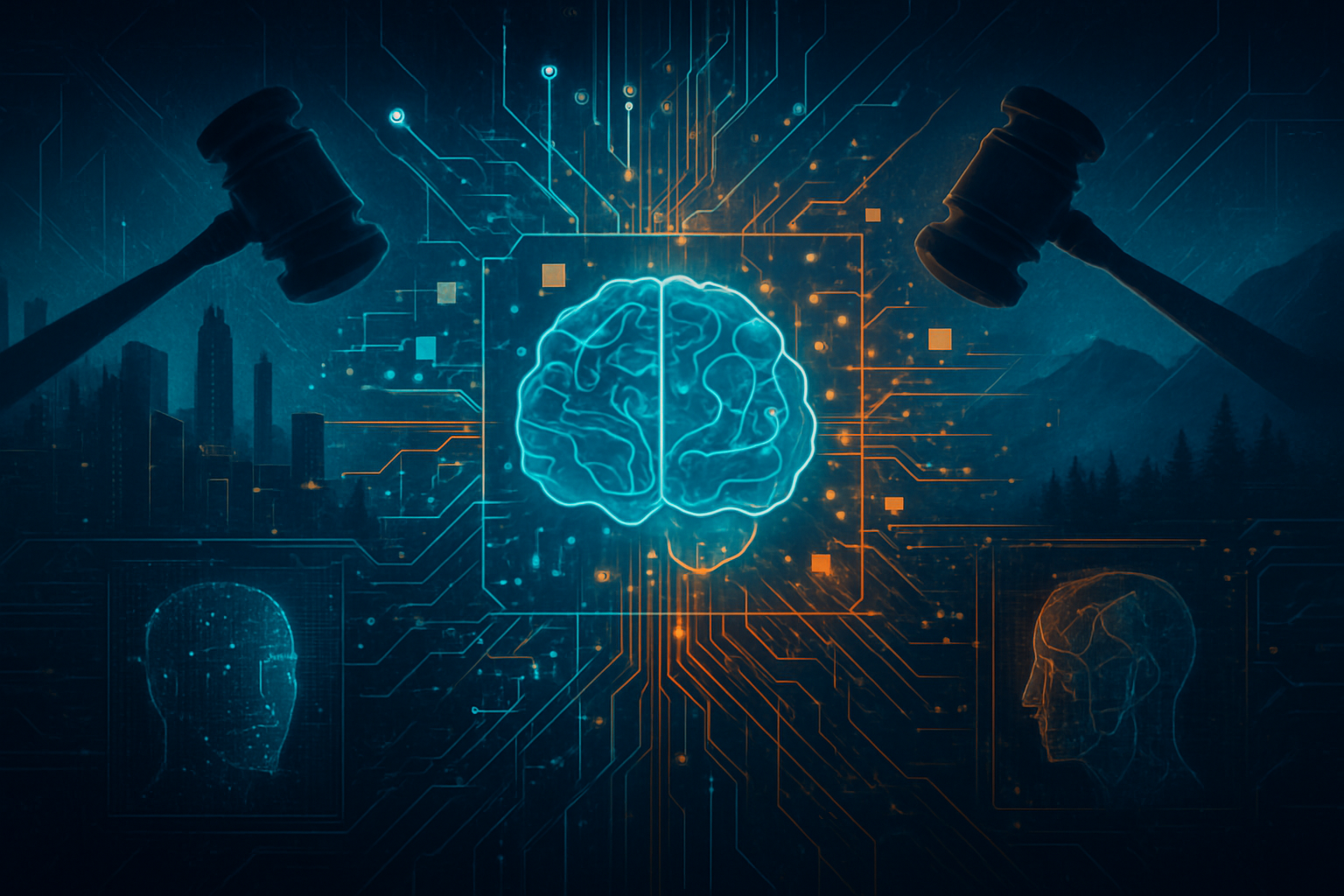
HARTFORD, Conn. — January 15, 2026 — The Travelers Companies, Inc. (NYSE: TRV) today announced a landmark expansion of its partnership with Anthropic, deploying the Claude 4 AI suite across its entire global workforce of more than 30,000 employees. This move represents one of the largest enterprise-wide integrations of generative AI in the financial services sector to date, signaling a definitive shift from experimental pilots to full-scale production in the insurance industry.
By weaving Anthropic’s most advanced models into its core operations, Travelers aims to reinvent the entire insurance value chain—from how it selects risks and processes claims to how it develops the software powering its $1.5 billion annual technology spend. The announcement marks a critical victory for Anthropic as it solidifies its reputation as the preferred AI partner for highly regulated, "stability-first" industries, positioning itself as a dominant counterweight to competitors in the enterprise space.
Technical Integration and Deployment Scope
The deployment is anchored by the Claude 4 model series, including Claude 4 Opus for complex reasoning and Claude 4 Sonnet for high-speed, intelligent workflows. Unlike standard chatbot implementations, Travelers has integrated these models into two distinct tiers. A specialized technical workforce of approximately 10,000 engineers, data scientists, and analysts is receiving personalized Claude AI assistants. These technical cohorts are utilizing Claude Code, a command-line interface (CLI)-based agent designed for autonomous, multi-step engineering tasks, which Travelers CTO Mojgan Lefebvre noted has already led to "meaningful improvements in productivity" by automating legacy code refactoring and machine learning model management.
For the broader workforce, the company has launched TravAI, a secure internal ecosystem that allows employees to leverage Claude’s capabilities within established safety guardrails. In claims processing, the integration has already yielded measurable results: an automated email classification system built on Amazon Bedrock (NASDAQ: AMZN) now categorizes millions of customer inquiries with 91% accuracy. This system has reportedly saved tens of thousands of manual hours, allowing claims professionals to focus on the human nuances of complex settlements rather than administrative triaging.
This rollout differs from previous industry approaches by utilizing "context-aware" models grounded in Travelers’ proprietary 65 billion data points. While earlier iterations like Claude 2 and Claude 3.5 were used for isolated pilot programs, the Claude 4 integration allows the AI to interpret unstructured data—including aerial imagery for property risk and complex medical bills—with a level of precision that mimics senior human underwriters. The industry has reacted with cautious optimism; AI research experts point to Travelers' "Responsible AI Framework" as a potential gold standard for navigating the intersection of deep learning and insurance ethics.
Competitive Dynamics and Market Positioning
The Travelers partnership significantly alters the competitive landscape of the AI sector. As of January 2026, Anthropic has captured approximately 40% of the enterprise Large Language Model (LLM) market, with a particularly strong 50% share in the AI coding segment. This deal highlights the growing divergence between Anthropic and OpenAI. While OpenAI remains the leader in the consumer market, Anthropic now generates roughly 85% of its revenue from business-to-business (B2B) contracts, appealing to firms that prioritize "Constitutional AI" and model steering over raw creative output.
For tech giants, the deal is a win-for-all-sides scenario. Anthropic’s valuation has soared to $350 billion following a recent funding round involving Microsoft (NASDAQ: MSFT) and Nvidia (NASDAQ: NVDA), despite Microsoft's deep-rooted ties to OpenAI. Simultaneously, the deployment on Amazon Bedrock reinforces Amazon’s position as the primary infrastructure layer for secure, serverless enterprise AI.
Within the insurance sector, the pressure on competitors is intensifying. While State Farm remains a leader in AI patents, the company is currently navigating legal challenges regarding "cheat-and-defeat" algorithms. In contrast, Travelers’ focus on interpretability and responsible AI provides a strategic marketing and regulatory advantage. Meanwhile, Progressive (NYSE: PGR) and Allstate (NYSE: ALL) find their traditional data moats—such as telematics—under threat as AI tools democratize the ability to analyze complex risk pools, forcing these giants to accelerate their own internal AI transformations.
Broader Significance and Regulatory Landscape
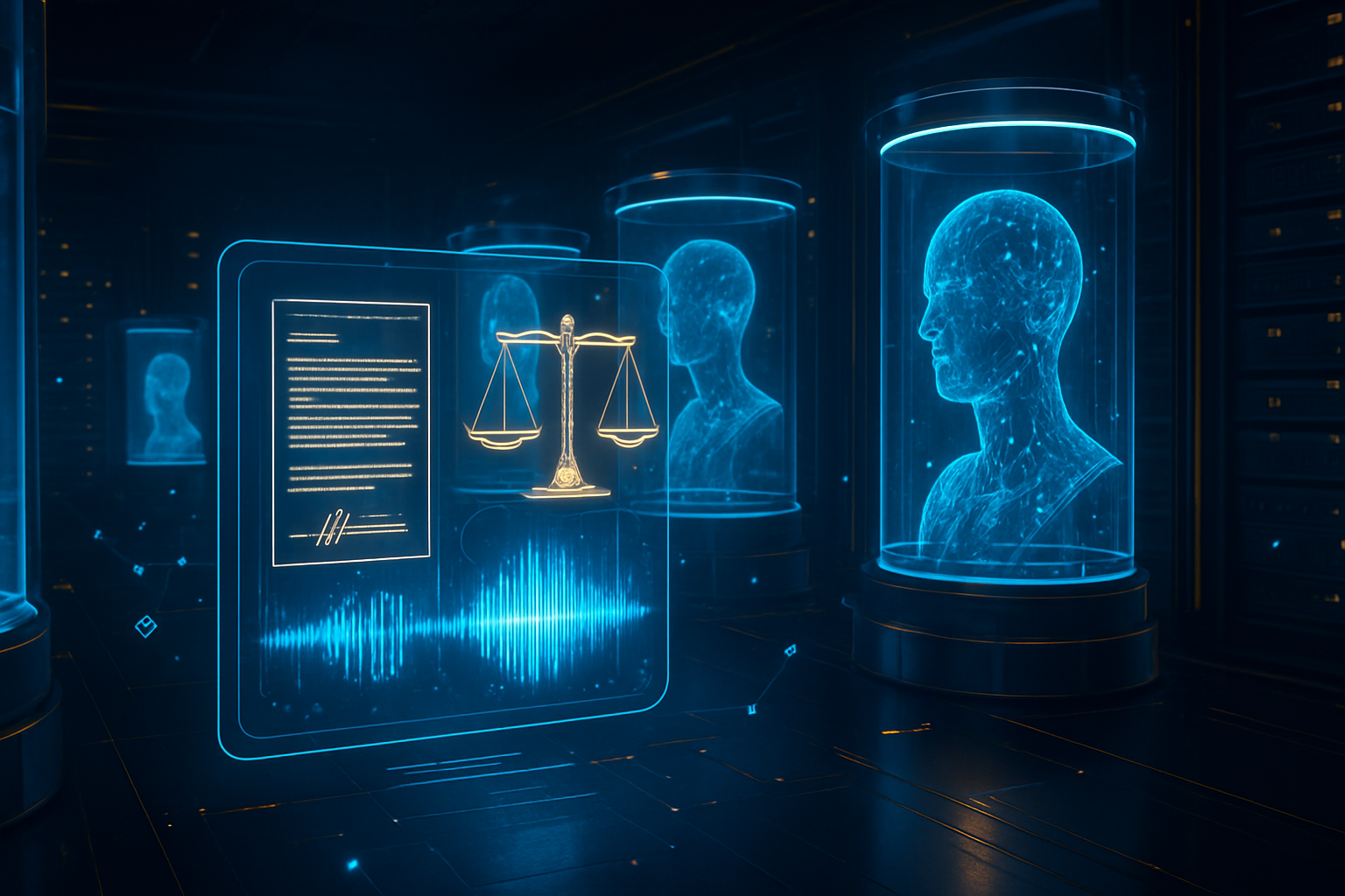
This partnership arrives at a pivotal moment in the global AI landscape. As of January 1, 2026, 38 U.S. states have enacted specific AI laws, creating a complex patchwork of transparency and bias-testing requirements. Travelers’ move to a unified, traceable AI system is a direct response to this regulatory climate. The industry is currently watching the conflict between the proposed federal "One Big Beautiful Bill Act," which seeks a moratorium on state-level AI rules, and the National Association of Insurance Commissioners (NAIC), which is pushing for localized, data-driven oversight.
The broader significance of the Travelers-Anthropic deal lies in the transformation of the insurer's identity. By moving toward real-time risk management rather than just reactive product provision, Travelers is following a trend seen in major global peers like Allianz (OTC: ALIZY). These firms are increasingly using AI as a defensive tool against emerging threats like deepfake fraud. In early 2026, many insurers began excluding deepfake-related losses from standard policies, making the ability to verify claims through AI a critical operational necessity rather than a luxury.
This milestone mirrors the "iPhone moment" for enterprise insurance. Just as mobile technology shifted insurance from paper to apps, the integration of Claude 4 shifts the industry from manual analysis to "agentic" operations, where AI doesn't just suggest a decision but prepares the entire workflow for human validation.
Future Outlook and Industry Challenges
Looking ahead, the near-term evolution of this partnership will likely focus on autonomous claims adjusting for high-frequency, low-severity events. Experts predict that by 2027, Travelers could compress its software development lifecycle for new products by as much as 50%, allowing the firm to launch hyper-targeted insurance products for niche risks like climate-driven micro-events in near real-time.
However, significant challenges remain. The industry must solve the "hallucination gap" in high-stakes underwriting, where a single incorrect AI inference could lead to millions in losses. Furthermore, as AI agents become more autonomous, the question of "legal personhood" for AI-driven decisions will likely reach the Supreme Court within the next two years. Anthropic is expected to address these concerns with even more robust "transparency layers" in its rumored Claude 5 release, anticipated late in 2026.
A Paradigm Shift in Insurance History
The Travelers-Anthropic partnership is a definitive signal that the era of AI experimentation is over. By equipping 30,000 employees with specialized AI agents, Travelers is making a $1.5 billion bet that the future of insurance belongs to the most "technologically agile" firms, not necessarily the ones with the largest balance sheets. The key takeaways are clear: Anthropic has successfully pivot-positioned itself as the "Gold Standard" for regulated enterprise AI, and the insurance industry is being forced into a rapid, AI-first consolidation.
In the history of AI, this deployment will likely be remembered as the moment when generative models became invisible, foundational components of the global financial infrastructure. In the coming months, the industry will be watching Travelers’ loss ratios and operational expenses closely to see if this massive investment translates into a sustainable competitive advantage. For now, the message to the rest of the Fortune 500 is loud and clear: adapt to the agentic era, or risk being out-underwritten by the machines.
This content is intended for informational purposes only and represents analysis of current AI developments.
TokenRing AI delivers enterprise-grade solutions for multi-agent AI workflow orchestration, AI-powered development tools, and seamless remote collaboration platforms.
For more information, visit https://www.tokenring.ai/.