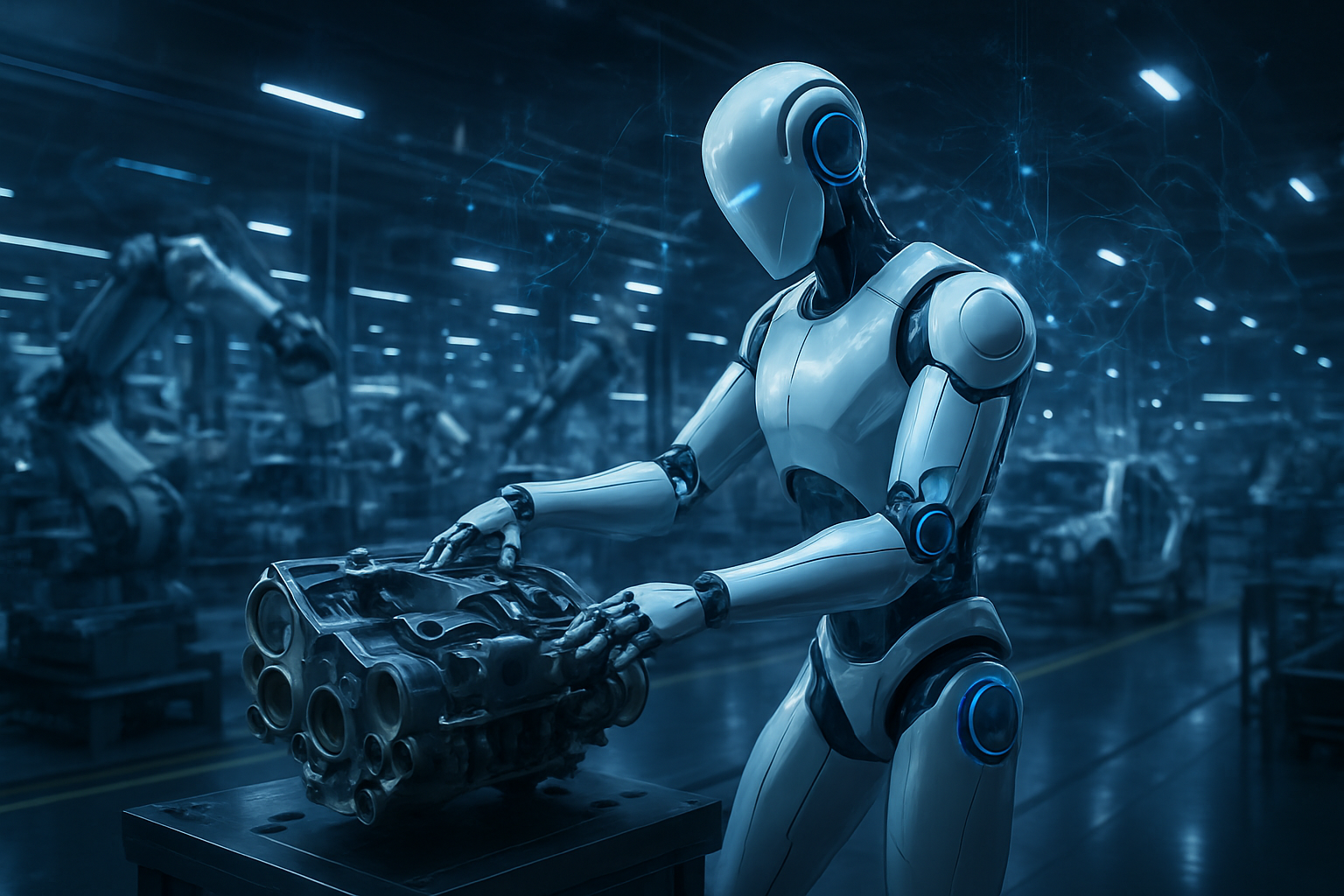
AUSTIN, TEXAS — January 14, 2026 — Tesla (NASDAQ: TSLA) has officially transitioned its humanoid robotics program from an ambitious experimental project to a pivotal component of its manufacturing workforce. Recent updates to the Optimus platform—specifically the deployment of the "Version 3" (Gen 3) hardware and FSD-v15 neural architecture—have demonstrated a level of human-like dexterity and autonomous navigation that was considered science fiction just 24 months ago. With thousands of units now integrated into the production lines for the upcoming "Cybercab" and the 4680 battery cells, Tesla is no longer just an automotive or energy company; it is rapidly becoming the world’s largest robotics firm.
The immediate significance of this development lies in the move away from teleoperation toward true, vision-based autonomy. Unlike earlier demonstrations that required human "puppeteers" for complex tasks, the early 2026 deployments show Optimus units independently identifying, picking, and placing delicate components with a failure rate lower than human trainees. This milestone signals the arrival of the "Physical AI" era, where large language models (LLMs) and computer vision converge to allow machines to navigate and manipulate the physical world with unprecedented grace.
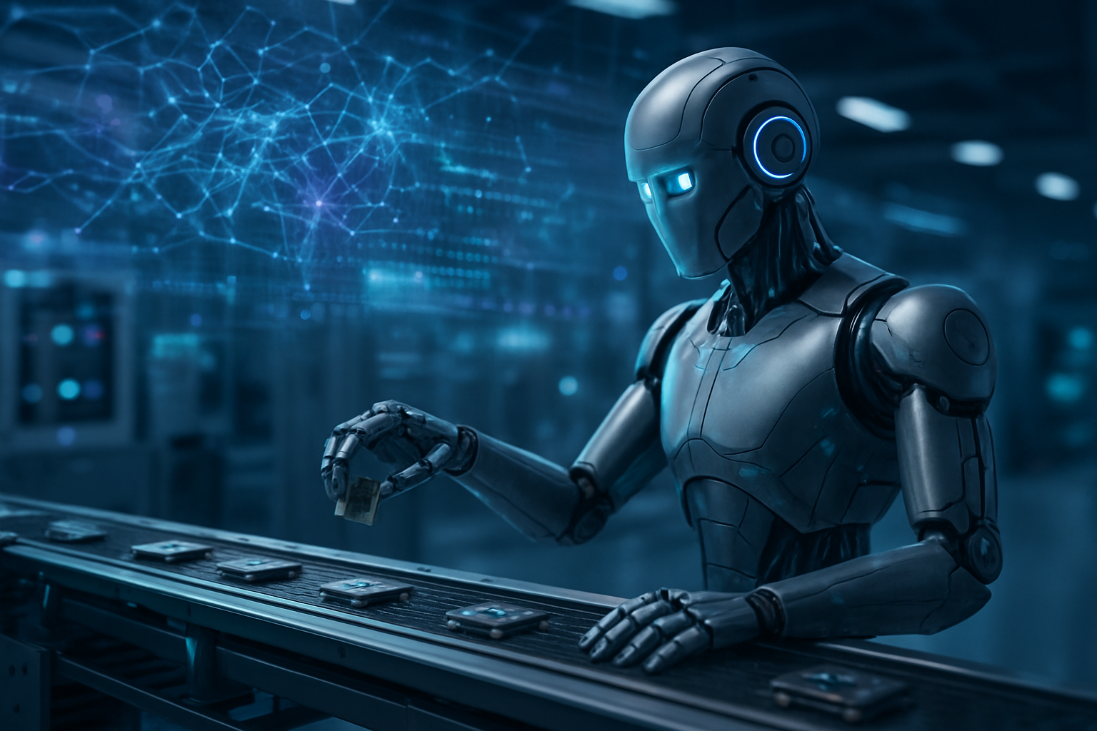
Precise Engineering: 22 Degrees of Freedom and "Squishy" Tactile Sensing
The technical specifications of the current Optimus Gen 3 platform represent a radical departure from the Gen 2 models seen in late 2024. The most striking advancement is the new humanoid hand. Moving from the previous 11 degrees of freedom (DoF), the Gen 3 hand now features 22 degrees of freedom, with actuators relocated to the forearm and connected via a sophisticated tendon-driven system. This mimics human muscle-tendon anatomy, allowing the robot to perform high-precision tasks such as threading electrical connectors or handling individual battery cells without the rigidity seen in traditional industrial arms.
Furthermore, Tesla has solved one of the most difficult challenges in robotics: tactile feedback. The robot’s fingers and palms are now covered in a multi-layered, "squishy" sensor skin that provides high-resolution haptic data. This compliance allows the robot to "feel" the friction and weight of an object, preventing it from crushing delicate items or dropping slippery ones. On the locomotion front, the robot has achieved a "jogging" gait, reaching speeds of up to 5–7 mph (2.4 m/s). This is powered by Tesla’s proprietary AI5 chip, which provides 40x the compute of the previous generation, enabling the robot to run real-time "Occupancy Networks" to navigate complex, bustling factory floors without a pre-mapped path.
Strategic Rivalry: A High-Stakes Race for the "Android Moment"
Tesla’s progress has ignited a fierce rivalry among tech giants and specialized robotics firms. Boston Dynamics, owned by Hyundai (OTC: HYMTF), recently unveiled its Production Electric Atlas, which boasts 56 degrees of freedom and is currently being deployed for heavy-duty parts sequencing in Hyundai’s smart factories. Meanwhile, Figure AI—backed by Microsoft (NASDAQ: MSFT) and NVIDIA (NASDAQ: NVDA)—has launched Figure 03, a robot that utilizes "Helix AI" to learn tasks simply by watching human videos. Unlike Optimus, which is focused on internal Tesla manufacturing, Figure is aggressively targeting the broader commercial logistics market, recently signing a major expansion deal with BMW (BMW.DE).
This development has profound implications for the AI industry at large. Companies like Alphabet (NASDAQ: GOOGL) are pivoting their DeepMind robotics research to provide the "brains" for third-party humanoid shells, while startups like Sanctuary AI are focusing on wheeled "Phoenix" models for stability in retail environments. Tesla’s strategic advantage remains its vertical integration; by manufacturing its own actuators, sensors, and AI chips, Tesla aims to drive the cost of an Optimus unit below $20,000, a price point that competitors using off-the-shelf components struggle to match.
Global Impact: The Dawn of the Post-Scarcity Economy?
The rise of Optimus fits into a broader trend of "Physical AI," where the intelligence previously confined to chatbots is given a body. This shift marks a major milestone, comparable to the "GPT-4 moment" for natural language. As these robots move from the lab to the factory, the primary concern is no longer if they will work, but how they will change the global labor market. Tesla CEO Elon Musk has framed this as a humanitarian mission, suggesting that Optimus will be the key to a "post-scarcity" world where the cost of goods drops dramatically as labor becomes an infinite resource.
However, this transition is not without its anxieties. Critics point to the potential for massive displacement of entry-level warehouse and manufacturing jobs. While industry analysts argue that the robots are solving a "demographic cliff" caused by aging workforces in the West and East Asia, the speed of the rollout has caught many labor regulators off guard. Ethical discussions are now shifting toward "robot taxes" and universal basic income (UBI), as the distinction between "human work" and "automated labor" begins to blur in the physical realm for the first time in history.
The Horizon: From Giga Texas to the Home
Looking ahead to late 2026 and 2027, Tesla plans to scale production to roughly 100,000 units per year. A dedicated humanoid production facility at Giga Texas is already under construction. In the near term, expect to see Optimus moving beyond the factory floor into more varied environments, such as construction sites or high-security facilities. The "Holy Grail" remains the consumer market; Musk has teased a "Home Assistant" version of Optimus that could eventually perform domestic chores like laundry and grocery retrieval.
The primary challenges remaining are battery life—currently limited to about 6–8 hours of active work—and the "edge case" problem in unstructured environments. While a factory is controlled, a suburban home is chaotic. Experts predict that the next two years will be spent refining the "General Purpose" nature of the AI, allowing the robot to reason through unexpected situations, such as a child running across its path or a spilled liquid on the floor, without needing a software update for every new scenario.
Conclusion: A Core Pillar of Future Value
In the January 2026 Q4 earnings call, Musk reiterated that Optimus represents approximately 80% of Tesla’s long-term value. This sentiment is reflected in the company’s massive capital expenditure on AI training clusters and the AI5 hardware suite. The journey from a man in a spandex suit in 2021 to a functional, 22-DoF autonomous humanoid in 2026 is one of the fastest technical evolutions in modern history.
As we look toward the "Humanoid Robotics World Championship" in Zurich later this year, it is clear that the race for physical autonomy has reached a fever pitch. Whether Optimus becomes the "biggest product of all time" remains to be seen, but its presence on the assembly lines of Giga Texas today proves that the humanoid era has officially begun. The coming months will be critical as Tesla begins to lease the first units to outside partners, testing if the "Optimus-as-a-Service" model can truly transform the global economy.
This content is intended for informational purposes only and represents analysis of current AI developments.
TokenRing AI delivers enterprise-grade solutions for multi-agent AI workflow orchestration, AI-powered development tools, and seamless remote collaboration platforms.
For more information, visit https://www.tokenring.ai/.