The semiconductor industry has officially entered the "Glass Age." As of early 2026, the long-standing physical limits of organic packaging materials have finally collided with the insatiable thermal and processing demands of generative AI, sparking a massive industry-wide pivot. Leading the charge are South Korean tech giants Samsung Electro-Mechanics (KRX: 009150) and LG Innotek (KRX: 011070), both of whom have accelerated their roadmaps to replace traditional plastic-based substrates with high-precision glass cores.
This transition is not merely an incremental upgrade; it is a fundamental architectural shift. Samsung Electro-Mechanics is currently on track to deliver its first commercial prototypes by the end of 2026, while LG Innotek has set a firm sights on 2028 for full-scale mass production. For the AI industry, which is currently struggling to scale hardware beyond the 1,000-watt threshold, glass substrates represent the "holy grail" of packaging—offering the structural integrity and electrical performance required to power the next generation of "super-chips."
Breaking the "Warpage Wall" with Glass Precision
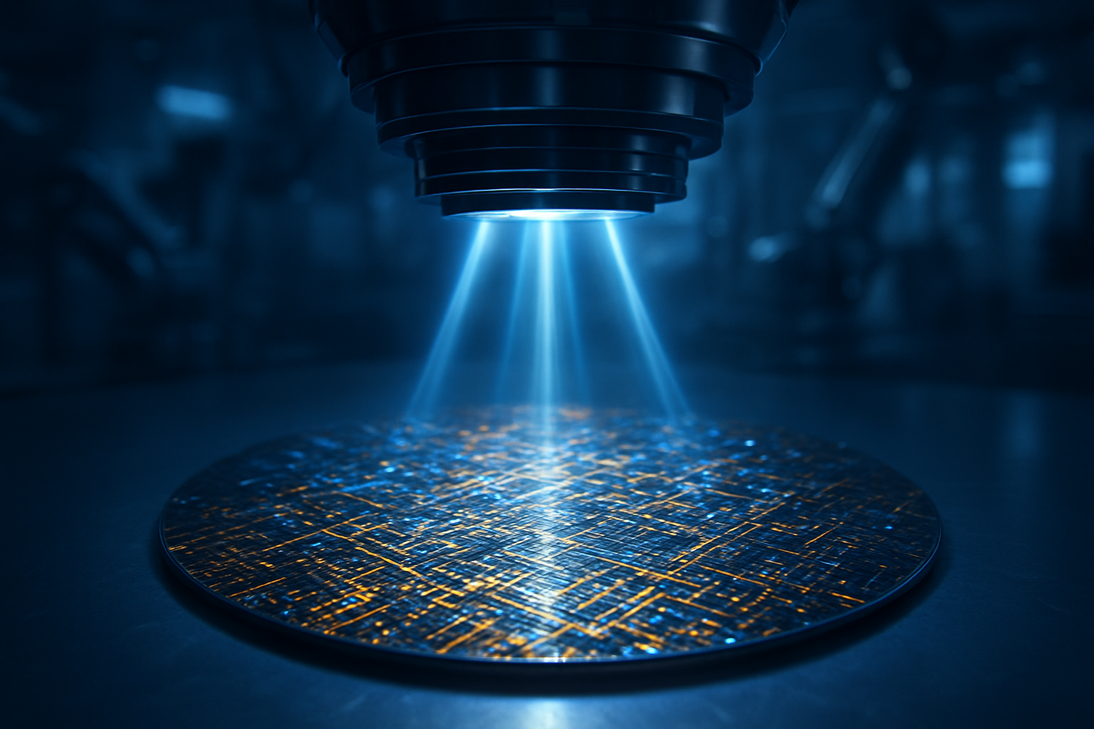
At the heart of this shift is a phenomenon known as the "warpage wall." For decades, the industry has relied on Ajinomoto Build-up Film (ABF), an organic, plastic-like material, to connect silicon chips to circuit boards. However, as AI accelerators from companies like NVIDIA (NASDAQ: NVDA) and AMD (NASDAQ: AMD) grow larger and hotter, these organic materials have reached their breaking point. Because organic substrates have a significantly higher Coefficient of Thermal Expansion (CTE) than the silicon they support, they physically warp and bend under extreme heat. This deformation leads to "cracked micro-bumps"—microscopic failures in the electrical connections that render the entire chip useless.
Glass substrates solve this by matching the CTE of silicon almost perfectly. By providing a substrate that remains ultra-flat even at temperatures exceeding those found in high-density data centers, manufacturers can build packages larger than 100mm x 100mm—a feat previously impossible with organic materials. Furthermore, glass allows for a "40% better signal integrity" profile, primarily through a dramatic reduction in signal loss. This efficiency enables data to move across the package with up to 50% lower power consumption, a critical metric for hyperscalers like Amazon (NASDAQ: AMZN) and Microsoft (NASDAQ: MSFT) who are battling rising energy costs in their AI infrastructures.
The technical superiority of glass also extends to interconnect density. Unlike organic substrates that require mechanical drilling, glass uses laser-etched Through-Glass Vias (TGVs). This allows for a 10-fold increase in the number of vertical connections, enabling designers to pack dozens of High Bandwidth Memory (HBM) stacks directly around a GPU. Industry experts have described this as a "once-in-a-generation" leap that effectively bypasses the physical scaling limits that once threatened the post-Moore’s Law era.
A Battle of Giants: Samsung vs. Intel vs. LG Innotek
The race for glass supremacy has created a new competitive frontier among the world’s largest semiconductor players. Samsung Electro-Mechanics has utilized a "Triple Alliance" strategy, drawing on the glass-processing expertise of Samsung Display and the chip-making prowess of Samsung Electronics to fast-track its Sejong-based pilot line. Samsung CEO Chang Duck-hyun recently noted that 2026 will be the "defining year" for the commercialization of these "dream substrates," positioning the company to be a primary supplier for the next wave of AI hardware.
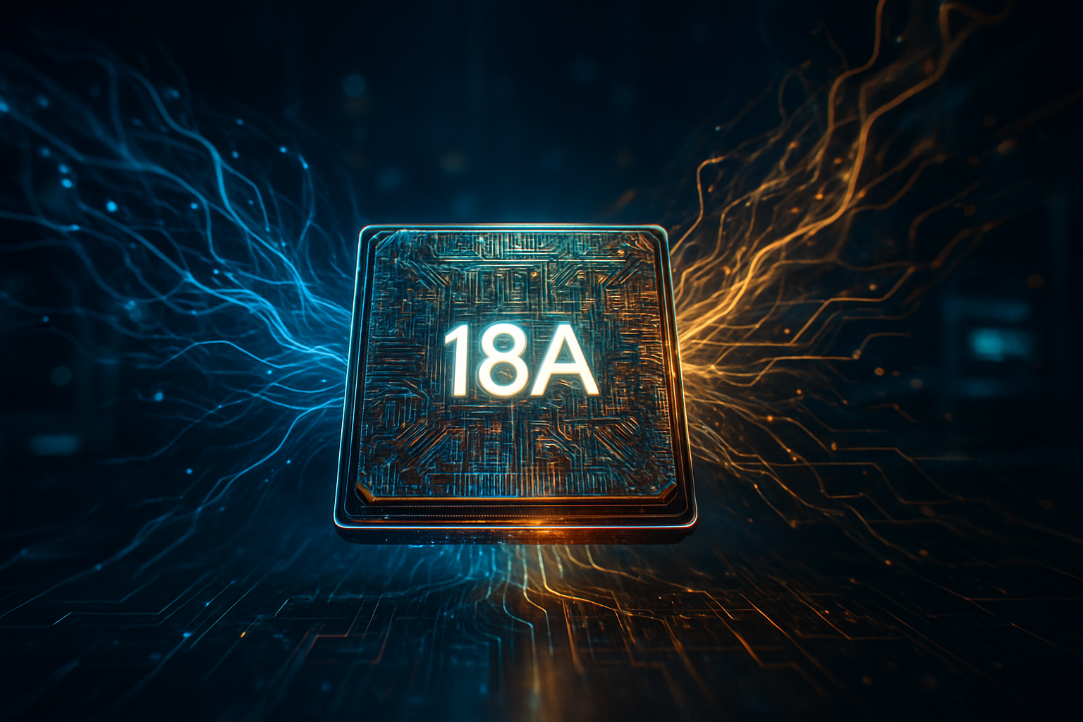
However, they are not alone. Intel (NASDAQ: INTC), an early pioneer in the space, has already moved into high-volume manufacturing (HVM) at its Arizona facility, aiming to integrate glass cores into its 18A and 14A process nodes. Meanwhile, LG Innotek is playing a more calculated long-game. While their mass production target is 2028, LG Innotek CEO Moon Hyuk-soo has emphasized that the company is focusing on solving the industry's most nagging problem: glass brittleness. "Whoever solves the issue of glass cracking first will lead the market," Moon stated during a recent industry summit, highlighting LG’s focus on durability and yield over immediate speed-to-market.
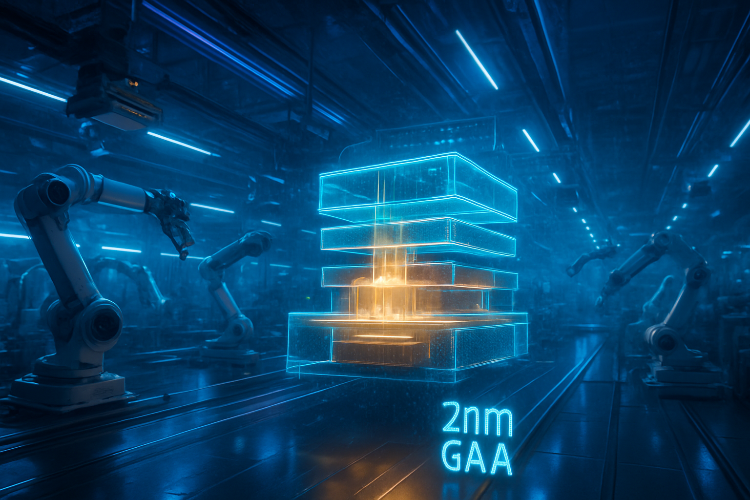
This competition is also drawing in traditional foundry leaders. TSMC (NYSE: TSM) has recently pivoted toward Fan-Out Panel-Level Packaging (FO-PLP) on glass to support future architectures like NVIDIA’s "Rubin" R100 GPUs. As these companies vie for dominance, the strategic advantage lies in who can most efficiently transition from 300mm circular wafers to massive 600mm x 600mm rectangular glass panels—a shift known as the "Rectangular Revolution" that promises to slash manufacturing costs while increasing usable area by over 80%.
The Wider Significance: Enabling the 1,000-Watt AI Era
The move to glass substrates is a direct response to the "energy wall" facing modern AI. As models grow more complex, the hardware required to train them has become increasingly power-hungry. Traditional packaging methods have become a bottleneck, both in terms of heat dissipation and the energy required just to move data between the processor and memory. By improving signal integrity and thermal management, glass substrates are essentially "widening the pipe" for AI computation, allowing for more performant chips that are simultaneously more energy-efficient.
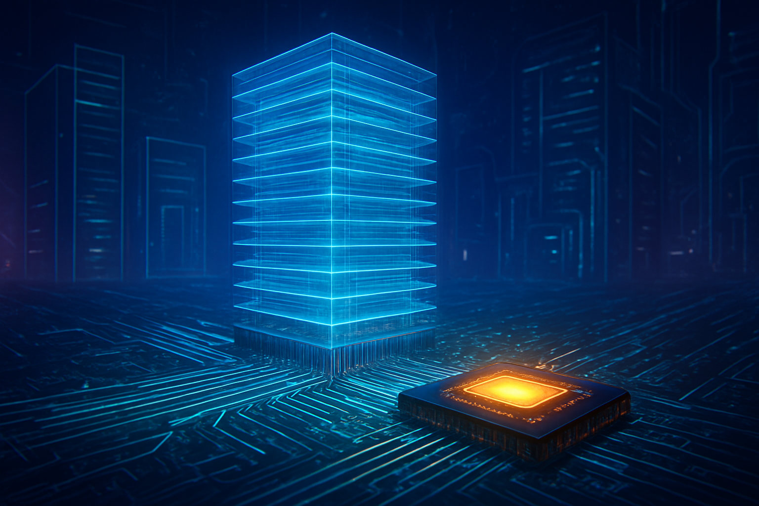
This shift also marks a broader trend toward "System-in-Package" (SiP) innovation. In the past, performance gains came primarily from shrinking transistors on the silicon itself. Today, as that process becomes exponentially more expensive and difficult, the industry is looking to the package—the "house" the chip lives in—to drive the next decade of performance. Glass is the foundation of this new house, enabling a modular "chiplet" approach where different types of processors and memory can be tiled together with near-zero latency.
However, the transition is not without its risks. The primary concern remains the inherent fragility of glass. While it is thermally stable, it is susceptible to "micro-cracks" during the manufacturing process, which can lead to catastrophic yield losses. The industry's ability to develop automated handling equipment that can manage these ultra-thin glass panels at scale will determine how quickly the technology trickles down from high-end AI servers to consumer electronics.
Future Developments and the Road to 2030
Looking ahead, the roadmap for glass substrates extends far beyond 2026. While the immediate focus is on 1,000-watt AI accelerators for data centers, analysts expect the technology to migrate into high-end laptops and mobile devices by the end of the decade. By 2028, when LG Innotek enters the fray with its mass-production lines, we may see the first "all-glass" mobile processors, which could offer significant battery life improvements due to the reduced power required for internal data movement.
The next two years will be characterized by rigorous testing and "qualification cycles." Hyperscalers are currently evaluating prototypes from Samsung and Absolics—a subsidiary of SKC (KRX: 011790)—to ensure these new substrates can survive the 24/7 high-heat environments of modern AI clusters. If these tests are successful, 2027 could see a massive "lift and shift" where glass becomes the standard for all high-performance computing (HPC) applications.
Experts also predict that the rise of glass substrates will trigger a wave of mergers and acquisitions in the materials science sector. Traditional chemical suppliers will need to adapt to a world where glass-handling equipment and laser-via technologies are as essential as the silicon itself. The "cracking problem" remains the final technical hurdle, but with the combined R&D budgets of Samsung, LG, and Intel focused on the issue, a solution is widely expected before the 2028 production window.
A New Foundation for Artificial Intelligence
The shift toward glass substrates represents one of the most significant changes in semiconductor packaging in over twenty years. By solving the "warpage wall" and providing a 40% boost to signal integrity, glass is providing the physical foundation upon which the next decade of AI breakthroughs will be built. Samsung Electro-Mechanics’ aggressive 2026 timeline and LG Innotek’s specialized 2028 roadmap show that the industry's heaviest hitters are fully committed to this "Glass Age."
As we move toward the end of 2026, the industry will be watching Samsung's pilot line in Sejong with intense scrutiny. Its success—or failure—to achieve high yields will serve as the first real-world test of whether glass can truly replace organic materials on a global scale. For now, the message from the semiconductor world is clear: the future of AI is no longer just about the silicon; it is about the glass that holds it all together.
This content is intended for informational purposes only and represents analysis of current AI developments.
TokenRing AI delivers enterprise-grade solutions for multi-agent AI workflow orchestration, AI-powered development tools, and seamless remote collaboration platforms.
For more information, visit https://www.tokenring.ai/.