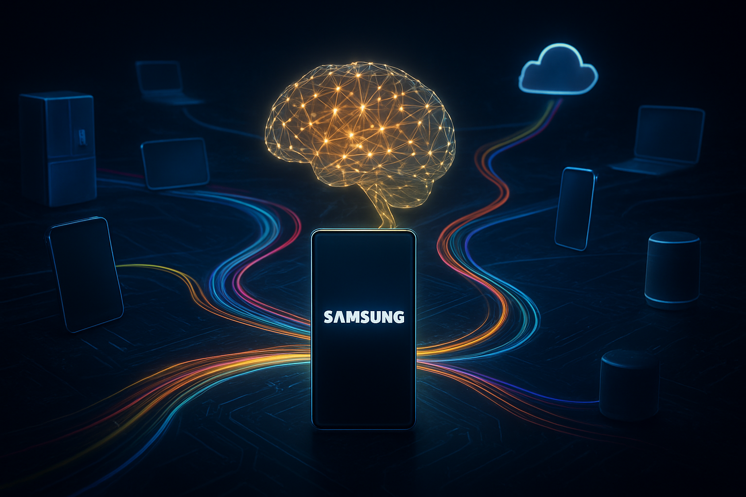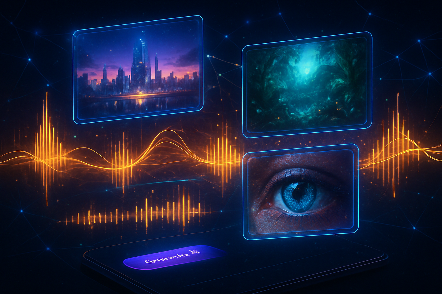
MENLO PARK, CA — As of January 12, 2026, the landscape of digital content has undergone a seismic shift, driven by the full-scale integration of Meta Platforms, Inc. (NASDAQ: META) and its revolutionary Movie Gen system. What began as a high-profile research announcement in late 2024 has evolved into the backbone of a new era of "Social Cinema." Movie Gen is no longer just a tool for tech enthusiasts; it is now a native feature within Instagram, Facebook, and WhatsApp, allowing billions of users to generate high-definition, 1080p video synchronized with cinematic, AI-generated sound effects and music with a single text prompt.
The immediate significance of Movie Gen lies in its unprecedented "personalization" capabilities. Unlike its predecessors, which focused on generic scene generation, Movie Gen allows users to upload a single reference image to generate videos featuring themselves in any imaginable scenario—from walking on the moon to starring in an 18th-century period drama. This development has effectively democratized high-end visual effects, placing the power of a Hollywood post-production studio into the pocket of every smartphone user.
The Architecture of Motion: Inside the 43-Billion Parameter Engine
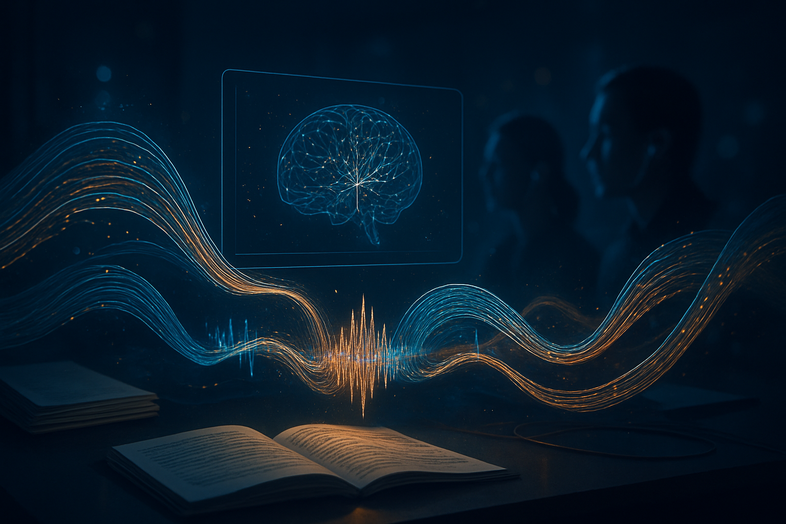
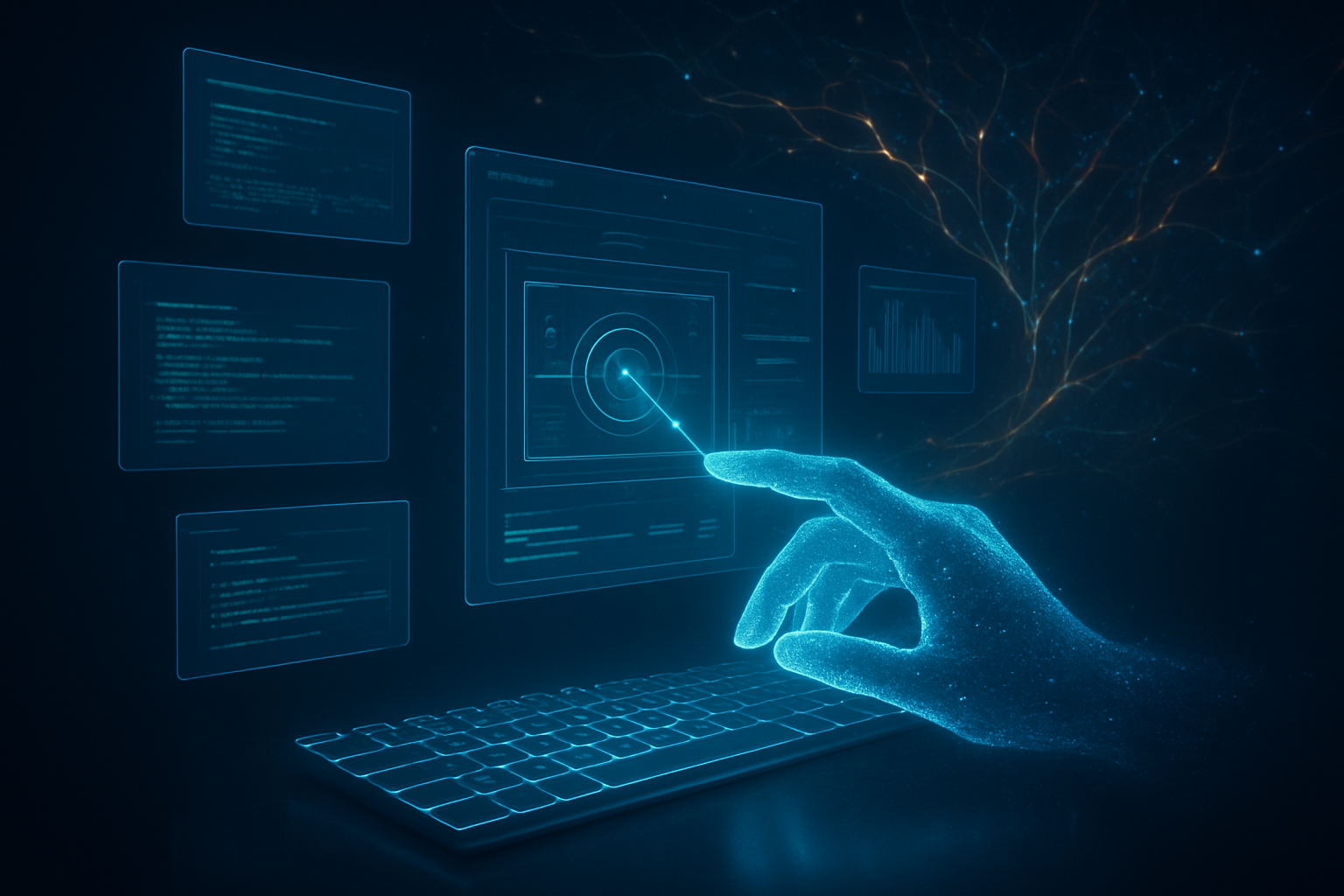
Technically, Movie Gen represents a departure from the pure diffusion models that dominated the early 2020s. The system is comprised of two primary foundation models: a 30-billion parameter video generation model and a 13-billion parameter audio model. Built on a Transformer-based architecture similar to the Llama series, Movie Gen utilizes a "Flow Matching" framework. This approach allows the model to learn the mathematical "flow" of pixels more efficiently than traditional diffusion, enabling the generation of 16-second continuous video clips at 16 to 24 frames per second.
What sets Movie Gen apart from existing technology is its "Triple Encoder" system. To ensure that a user’s prompt is followed with surgical precision, Meta employs three distinct encoders: UL2 for logical reasoning, MetaCLIP for visual alignment, and ByT5 for rendering specific text or numbers within the video. Furthermore, the system operates within a unified latent space, ensuring that audio—such as the crunch of gravel or a synchronized orchestral swell—is perfectly timed to the visual action. This native synchronization eliminates the "uncanny silence" that plagued earlier AI video tools.
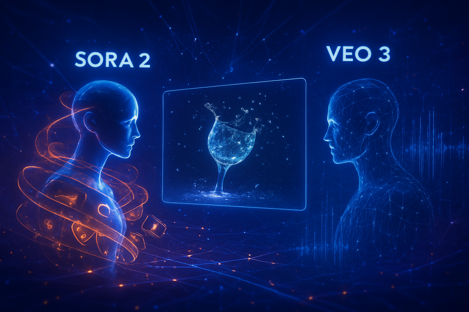
The AI research community has lauded Meta's decision to move toward a spatio-temporal tokenization method, which treats a 16-second video as a sequence of roughly 73,000 tokens. Industry experts note that while competitors like OpenAI’s Sora 2 may offer longer narrative durations, Meta’s "Magic Edits" feature—which allows users to modify specific elements of an existing video using text—is currently the gold standard for precision. This allows for "pixel-perfect" alterations, such as changing a character's clothing or the time of day, without distorting the rest of the scene.
Strategic Dominance: How Meta is Winning the AI Video Arms Race
The deployment of Movie Gen has solidified Meta’s (NASDAQ: META) position as the "Operating System of Social Entertainment." By integrating these models directly into its ad-buying platform, Andromeda, Meta has revolutionized the $600 billion digital advertising market. Small businesses can now use Movie Gen to auto-generate thousands of high-fidelity video ad variants in real-time, tailored to the specific interests of individual viewers. Analysts at major firms have recently raised Meta’s price targets, citing a 20% increase in conversion rates for AI-generated video ads compared to traditional static content.
However, the competition remains fierce. ByteDance (the parent company of TikTok) has countered with its Seedance 1.0 model, which is currently being offered for free via the CapCut editing suite to maintain its grip on the younger demographic. Meanwhile, startups like Runway and Pika have pivoted toward the professional "Pro-Sumer" market. Runway’s Gen-4.5, for instance, offers granular camera controls and "Physics-First" motion that still outperforms Meta in high-stakes cinematic environments. Despite this, Meta’s massive distribution network gives it a strategic advantage that specialized startups struggle to match.
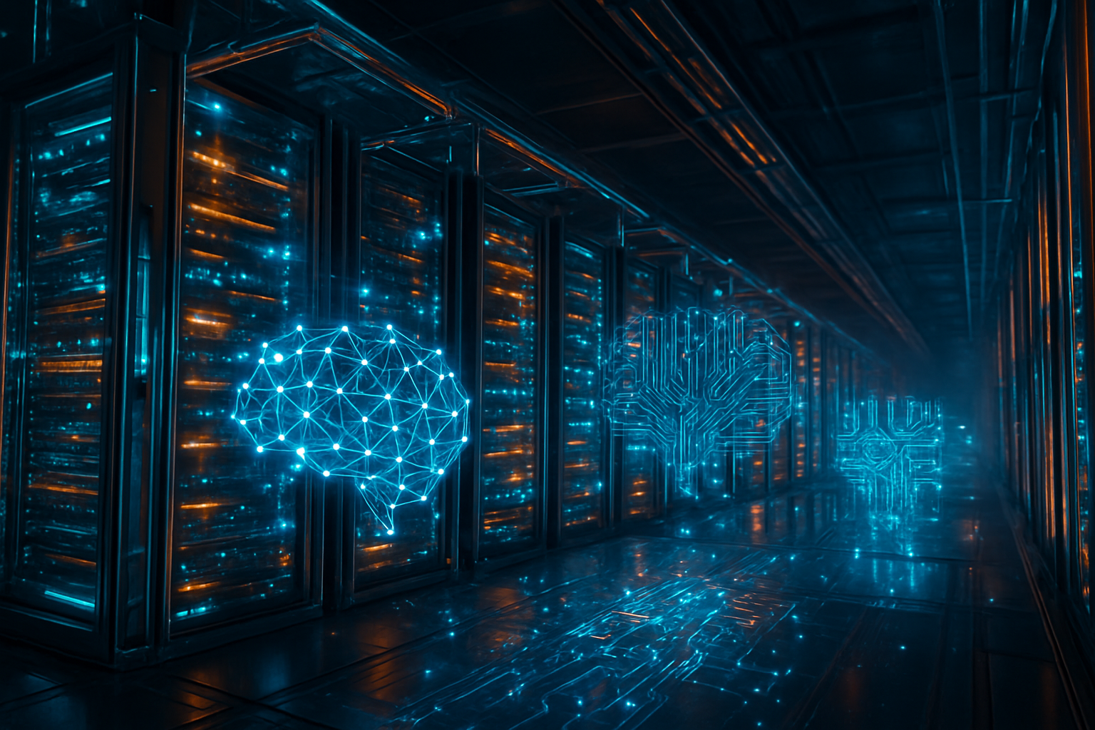
The disruption to existing services is most evident in the stock performance of traditional stock footage companies and mid-tier VFX houses. As Movie Gen makes "generic" cinematic content free and instant, these industries are being forced to reinvent themselves as "AI-augmentation" services. Meta’s vertical integration—extending from its own custom MTIA silicon to its recent nuclear energy partnerships to power its massive data centers—ensures that it can run these compute-heavy models at a scale its competitors find difficult to subsidize.
Ethical Fault Lines and the "TAKE IT DOWN" Era
The wider significance of Movie Gen extends far beyond entertainment, touching on the very nature of digital truth. As we enter 2026, the "wild west" of generative AI has met its first major regulatory hurdles. The U.S. federal government’s TAKE IT DOWN Act, enacted in mid-2025, now mandates that Meta remove non-consensual deepfakes within 48 hours. In response, Meta has pioneered the use of C2PA "Content Credentials," invisible watermarks that are "soft-bound" to every Movie Gen file, allowing third-party platforms to identify AI-generated content instantly.
Copyright remains a contentious battlefield. Meta is currently embroiled in a high-stakes $350 million lawsuit with Strike 3 Holdings, which alleges that Meta trained its models on pirated cinematic data. This case is expected to set a global precedent for "Fair Use" in the age of generative media. If the courts rule against Meta, it could force a massive restructuring of how AI models are trained, potentially requiring "opt-in" licenses for every frame of video used in training sets.
Labor tensions also remain high. The 2026 Hollywood labor negotiations have been dominated by the "StrikeWatch '26" movement, as guilds like SAG-AFTRA seek protection against "digital doubles." While Meta has partnered with Blumhouse Productions to showcase Movie Gen as a tool for "cinematic co-direction," rank-and-file creators fear that the democratization of video will lead to a "race to the bottom" in wages, where human creativity is valued less than algorithmic efficiency.
The Horizon: 4K Real-Time Generation and Beyond
Looking toward the near future, experts predict that Meta will soon unveil "Movie Gen 4K," a model capable of producing theater-quality resolution in real-time. The next frontier is interactive video—where the viewer is no longer a passive observer but can change the plot or setting of a video as it plays. This "Infinite Media" concept could merge the worlds of social media, gaming, and traditional film into a single, seamless experience.
The primary challenge remains the "physics problem." While Movie Gen is adept at textures and lighting, complex fluid dynamics and intricate human hand movements still occasionally exhibit "hallucinations." Addressing these technical hurdles will require even more massive datasets and compute power. Furthermore, as AI-generated content begins to flood the internet, Meta faces the challenge of "Model Collapse," where AI models begin training on their own outputs, potentially leading to a degradation in creative original thought.
A New Chapter in the History of Media
The full release of Meta Movie Gen marks a definitive turning point in the history of artificial intelligence. It represents the moment AI transitioned from generating static images and text to mastering the complex, multi-modal world of synchronized sight and sound. Much like the introduction of the smartphone or the internet itself, Movie Gen has fundamentally altered how humans tell stories and how brands communicate with consumers.
In the coming months, the industry will be watching closely as the first "Movie Gen-native" feature films begin to appear on social platforms. The long-term impact will likely be a total blurring of the line between "creator" and "consumer." As Meta continues to refine its models, the question is no longer whether AI can create art, but how human artists will evolve to stay relevant in a world where the imagination is the only limit to production.
This content is intended for informational purposes only and represents analysis of current AI developments.
TokenRing AI delivers enterprise-grade solutions for multi-agent AI workflow orchestration, AI-powered development tools, and seamless remote collaboration platforms.
For more information, visit https://www.tokenring.ai/.