Blog

  • The ‘USB-C for AI’: How Anthropic’s MCP and Enterprise Agent Skills are Standardizing the Agentic Era

    The ‘USB-C for AI’: How Anthropic’s MCP and Enterprise Agent Skills are Standardizing the Agentic Era

    As of early 2026, the artificial intelligence landscape has shifted from a race for larger models to a race for more integrated, capable agents. At the center of this transformation is Anthropic’s Model Context Protocol (MCP), a revolutionary open standard that has earned the moniker "USB-C for AI." By creating a universal interface for AI models to interact with data and tools, Anthropic has effectively dismantled the walled gardens that previously hindered agentic workflows. The recent launch of "Enterprise Agent Skills" has further accelerated this trend, providing a standardized framework for agents to execute complex, multi-step tasks across disparate corporate databases and APIs.

    The significance of this development cannot be overstated. Before the widespread adoption of MCP, connecting an AI agent to a company’s proprietary data—such as a SQL database or a Slack workspace—required custom, brittle code for every unique integration. Today, MCP acts as the foundational "plumbing" of the AI ecosystem, allowing any model to "plug in" to any data source that supports the standard. This shift from siloed AI to an interoperable agentic framework marks the beginning of the "Digital Coworker" era, where AI agents operate with the same level of access and procedural discipline as human employees.

    The Model Context Protocol (MCP) operates on a sleek client-server architecture designed to solve the "fragmentation problem." At its core, an MCP server acts as a translator between an AI model and a specific data source or tool. While the initial 2024 launch focused on basic connectivity, the 2025 introduction of Enterprise Agent Skills added a layer of "procedural intelligence." These Skills are filesystem-based modules containing structured metadata, validation scripts, and reference materials. Unlike simple prompts, Skills allow agents to understand how to use a tool, not just that the tool exists. This technical specification ensures that agents follow strict corporate protocols when performing tasks like financial auditing or software deployment.

    One of the most critical technical advancements within the MCP ecosystem is "progressive disclosure." To prevent the common "Lost in the Middle" phenomenon—where LLMs lose accuracy as context windows grow too large—Enterprise Agent Skills use a tiered loading system. The agent initially only sees a lightweight metadata description of a skill. It only "loads" the full technical documentation or specific reference files when they become relevant to the current step of a task. This dramatically reduces token consumption and increases the precision of the agent's actions, allowing it to navigate terabytes of data without overwhelming its internal memory.

    Furthermore, the protocol now emphasizes secure execution through virtual machine (VM) sandboxing. When an agent utilizes a Skill to process sensitive data, the code can be executed locally within a secure environment. Only the distilled, relevant results are passed back to the large language model (LLM), ensuring that proprietary raw data never leaves the enterprise's secure perimeter. This architecture differs fundamentally from previous "prompt-stuffing" approaches, offering a scalable, secure, and cost-effective way to deploy agents at the enterprise level. Initial reactions from the research community have been overwhelmingly positive, with many experts noting that MCP has effectively become the "HTTP of the agentic web."

    The strategic implications of MCP have triggered a massive realignment among tech giants. While Anthropic pioneered the protocol, its decision to donate MCP to the Agentic AI Foundation (AAIF) under the Linux Foundation in late 2025 was a masterstroke that secured its future. Microsoft (NASDAQ: MSFT) was among the first to fully integrate MCP into Windows 11 and Azure AI Foundry, signaling that the standard would be the backbone of its "Copilot" ecosystem. Similarly, Alphabet (NASDAQ: GOOGL) has adopted MCP for its Gemini models, offering managed MCP servers that allow enterprise customers to bridge their Google Cloud data with any compliant AI agent.

    The adoption extends beyond the traditional "Big Tech" players. Amazon (NASDAQ: AMZN) has optimized its custom Trainium chips to handle the high-concurrency workloads typical of MCP-heavy agentic swarms, while integrating the protocol directly into Amazon Bedrock. This move positions AWS as the preferred infrastructure for companies running massive fleets of interoperable agents. Meanwhile, companies like Block (NYSE: SQ) have contributed significant open-source frameworks, such as the Goose agent, which utilizes MCP as its primary connectivity layer. This unified front has created a powerful network effect: as more SaaS providers like Atlassian (NASDAQ: TEAM) and Salesforce (NYSE: CRM) launch official MCP servers, the value of being an MCP-compliant model increases exponentially.

    For startups, the "USB-C for AI" standard has lowered the barrier to entry for building specialized agents. Instead of spending months building integrations for every popular enterprise app, a startup can build one MCP-compliant agent that instantly gains access to the entire ecosystem of MCP-enabled tools. This has led to a surge in "Agentic Service Providers" that focus on fine-tuning specific skills—such as legal discovery or medical coding—rather than building the underlying connectivity. The competitive advantage has shifted from who has the data to who has the most efficient skills for processing that data.

    The rise of MCP and Enterprise Agent Skills fits into a broader trend of "Agentic Orchestration," where the focus is no longer on the chatbot but on the autonomous workflow. By early 2026, we are seeing the results of this shift: a move away from the "Token Crisis." Previously, the cost of feeding massive amounts of data into an LLM was a major bottleneck for enterprise adoption. By using MCP to fetch only the necessary data points on demand, companies have reduced their AI operational costs by as much as 70%, making large-scale agent deployment economically viable for the first time.

    However, this level of autonomy brings significant concerns regarding governance and security. The "USB-C for AI" analogy also highlights a potential vulnerability: if an agent can plug into anything, the risk of unauthorized data access or accidental system damage increases. To mitigate this, the 2026 MCP specification includes a mandatory "Human-in-the-Loop" (HITL) protocol for high-risk actions. This allows administrators to set "governance guardrails" where an agent must pause and request human authorization before executing an API call that involves financial transfers or permanent data deletion.

    Comparatively, the launch of MCP is being viewed as a milestone similar to the introduction of the TCP/IP protocol for the internet. Just as TCP/IP allowed disparate computer networks to communicate, MCP is allowing disparate "intelligence silos" to collaborate. This standardization is the final piece of the puzzle for the "Agentic Web," a future where AI agents from different companies can negotiate, share data, and complete complex transactions on behalf of their human users without manual intervention.

    Looking ahead, the next frontier for MCP and Enterprise Agent Skills lies in "Cross-Agent Collaboration." We expect to see the emergence of "Agent Marketplaces" where companies can purchase or lease highly specialized skills developed by third parties. For instance, a small accounting firm might "rent" a highly sophisticated Tax Compliance Skill developed by a top-tier global consultancy, plugging it directly into their MCP-compliant agent. This modularity will likely lead to a new economy centered around "Skill Engineering."

    In the near term, we anticipate a deeper integration between MCP and edge computing. As agents become more prevalent on mobile devices and IoT hardware, the need for lightweight MCP servers that can run locally will grow. Challenges remain, particularly in the realm of "Semantic Collisions"—where two different skills might use the same command to mean different things. Standardizing the vocabulary of these skills will be a primary focus for the Agentic AI Foundation throughout 2026. Experts predict that by 2027, the majority of enterprise software will be "Agent-First," with traditional user interfaces taking a backseat to MCP-driven autonomous interactions.

    The evolution of Anthropic’s Model Context Protocol into a global open standard marks a definitive turning point in the history of artificial intelligence. By providing the "USB-C" for the AI era, MCP has solved the interoperability crisis that once threatened to stall the progress of agentic technology. The addition of Enterprise Agent Skills has provided the necessary procedural framework to move AI from a novelty to a core component of enterprise infrastructure.

    The key takeaway for 2026 is that the era of "Siloed AI" is over. The winners in this new landscape will be the companies that embrace openness and contribute to the growing ecosystem of MCP-compliant tools and skills. As we watch the developments in the coming months, the focus will be on how quickly traditional industries—such as manufacturing and finance—can transition their legacy systems to support this new standard.

    Ultimately, MCP is more than just a technical protocol; it is a blueprint for how humans and AI will interact in a hyper-connected world. By standardizing the way agents access data and perform tasks, Anthropic and its partners in the Agentic AI Foundation have laid the groundwork for a future where AI is not just a tool we use, but a seamless extension of our professional and personal capabilities.


    This content is intended for informational purposes only and represents analysis of current AI developments.

    TokenRing AI delivers enterprise-grade solutions for multi-agent AI workflow orchestration, AI-powered development tools, and seamless remote collaboration platforms.
    For more information, visit https://www.tokenring.ai/.

  • Gemini 3 Flash: Reclaiming the Search Throne with Multimodal Speed

    Gemini 3 Flash: Reclaiming the Search Throne with Multimodal Speed

    In a move that marks the definitive end of the "ten blue links" era, Alphabet Inc. (NASDAQ: GOOGL) has officially completed the global rollout of Gemini 3 Flash as the default engine for Google Search’s "AI Mode." Launched in late December 2025 and reaching full scale as of January 5, 2026, the new model represents a fundamental pivot for the world’s most dominant gateway to information. By prioritizing "multimodal speed" and complex reasoning, Google is attempting to silence critics who argued the company had grown too slow to compete with the rapid-fire releases from Silicon Valley’s more agile AI labs.

    The immediate significance of Gemini 3 Flash lies in its unique balance of efficiency and "frontier-class" intelligence. Unlike its predecessors, which often forced users to choose between the speed of a lightweight model and the depth of a massive one, Gemini 3 Flash utilizes a new "Dynamic Thinking" architecture to deliver near-instantaneous synthesis of live web data. This transition marks the most aggressive change to Google’s core product since its inception, effectively turning the search engine into a real-time reasoning agent capable of answering PhD-level queries in the blink of an eye.

    Technical Coverage: The "Dynamic Thinking" Architecture

    Technically, Gemini 3 Flash is a departure from the traditional transformer-based scaling laws that defined the previous year of AI development. The model’s "Dynamic Thinking" architecture allows it to modulate its internal reasoning cycles based on the complexity of the prompt. For a simple weather query, the model responds with minimal latency; however, when faced with complex logic, it generates hidden "thinking tokens" to verify its own reasoning before outputting a final answer. This capability has allowed Gemini 3 Flash to achieve a staggering 33.7% on the "Humanity’s Last Exam" (HLE) benchmark without tools, and 43.5% when integrated with its search and code execution modules.

    This performance on HLE—a benchmark designed by the Center for AI Safety (CAIS) to be virtually unsolvable by models that rely on simple pattern matching—places Gemini 3 Flash in direct competition with much larger "frontier" models like GPT-5.2. While previous iterations of the Flash series struggled to break the 11% barrier on HLE, the version 3 release triples that capability. Furthermore, the model boasts a 1-million-token context window and can process up to 8.4 hours of audio or massive video files in a single prompt, allowing for multimodal search queries that were technically impossible just twelve months ago.

    Initial reactions from the AI research community have been largely positive, particularly regarding the model’s efficiency. Experts note that Gemini 3 Flash is roughly 3x faster than the Gemini 2.5 Pro while utilizing 30% fewer tokens for everyday tasks. This efficiency is not just a technical win but a financial one, as Google has priced the model at a competitive $0.50 per 1 million input tokens for developers. However, some researchers caution that the "synthesis" approach still faces hurdles with "low-data-density" queries, where the model occasionally hallucinates connections in niche subjects like hyper-local history or specialized culinary recipes.

    Market Impact: The End of the Blue Link Era

    The shift to Gemini 3 Flash as a default synthesis engine has sent shockwaves through the competitive landscape. For Alphabet Inc., this is a high-stakes gamble to protect its search monopoly against the rising tide of "answer engines" like Perplexity and the AI-enhanced Bing from Microsoft (NASDAQ: MSFT). By integrating its most advanced reasoning capabilities directly into the search bar, Google is leveraging its massive distribution advantage to preempt the user churn that analysts predicted would decimate traditional search traffic.

    This development is particularly disruptive to the SEO and digital advertising industry. As Google moves from a directory of links to a synthesis engine that provides direct, cited answers, the traditional flow of traffic to third-party websites is under threat. Gartner has already projected a 25% decline in traditional search volume by the end of 2026. Companies that rely on "top-of-funnel" informational clicks are being forced to pivot toward "agent-optimized" content, as Gemini 3 Flash increasingly acts as the primary consumer of web information, distilling it for the end user.

    For startups and smaller AI labs, the launch of Gemini 3 Flash raises the barrier to entry significantly. The model’s high performance on the SWE-bench (78.0%), which measures agentic coding tasks, suggests that Google is moving beyond search and into the territory of AI-powered development tools. This puts pressure on specialized coding assistants and agentic platforms, as Google’s "Antigravity" development platform—powered by Gemini 3 Flash—aims to provide a seamless, integrated environment for building autonomous AI agents at a fraction of the previous cost.

    Wider Significance: A Milestone on the Path to AGI

    Beyond the corporate horse race, the emergence of Gemini 3 Flash and its performance on Humanity's Last Exam signals a broader shift in the AGI (Artificial General Intelligence) trajectory. HLE was specifically designed to be "the final yardstick" for academic and reasoning-based knowledge. The fact that a "Flash" or mid-tier model is now scoring in the 40th percentile—nearing the 90%+ scores of human PhDs—suggests that the window for "expert-level" reasoning is closing faster than many anticipated. We are moving out of the era of "stochastic parrots" and into the era of "expert synthesizers."

    However, this transition brings significant concerns regarding the "atrophy of thinking." As synthesis engines become the default mode of information retrieval, there is a risk that users will stop engaging with source material altogether. The "AI-Frankenstein" effect, where the model synthesizes disparate and sometimes contradictory facts into a cohesive but incorrect narrative, remains a persistent challenge. While Google’s SynthID watermarking and grounding techniques aim to mitigate these risks, the sheer speed and persuasiveness of Gemini 3 Flash may make it harder for the average user to spot subtle inaccuracies.

    Comparatively, this milestone is being viewed by some as the "AlphaGo moment" for search. Just as AlphaGo proved that machines could master intuition-based games, Gemini 3 Flash is proving that machines can master the synthesis of the entire sum of human knowledge. The shift from "retrieval" to "reasoning" is no longer a theoretical goal; it is a live product being used by billions of people daily, fundamentally changing how humanity interacts with the digital world.

    Future Outlook: From Synthesis to Agency

    Looking ahead, the near-term focus for Google will likely be the refinement of "agentic search." With the infrastructure of Gemini 3 Flash in place, the next step is the transition from an engine that tells you things to an engine that does things for you. Experts predict that by late 2026, Gemini will not just synthesize a travel itinerary but will autonomously book the flights, handle the cancellations, and negotiate refunds using its multimodal reasoning capabilities.

    The primary challenge remaining is the "reasoning wall"—the gap between the 43% score on HLE and the 90%+ score required for true human-level expertise across all domains. Addressing this will likely require the launch of Gemini 4, which is rumored to incorporate "System 2" thinking even more deeply into its core architecture. Furthermore, as the cost of these models continues to drop, we can expect to see Gemini 3 Flash-class intelligence embedded in everything from wearable glasses to autonomous vehicles, providing real-time multimodal synthesis of the physical world.

    Conclusion: A New Standard for Information Retrieval

    The launch of Gemini 3 Flash is more than just a model update; it is a declaration of intent from Google. By reclaiming the search throne with a model that prioritizes both speed and PhD-level reasoning, Alphabet Inc. has reasserted its dominance in an increasingly crowded field. The key takeaways from this release are clear: the "blue link" search engine is dead, replaced by a synthesis engine that reasons as it retrieves. The high scores on the HLE benchmark prove that even "lightweight" models are now capable of handling the most difficult questions humanity can devise.

    In the coming weeks and months, the industry will be watching closely to see how OpenAI and Microsoft respond. With GPT-5.2 and Gemini 3 Flash now locked in a dead heat on reasoning benchmarks, the next frontier will likely be "reliability." The winner of the AI race will not just be the company with the fastest model, but the one whose synthesized answers can be trusted implicitly. For now, Google has regained the lead, turning the "search" for information into a conversation with a global expert.


    This content is intended for informational purposes only and represents analysis of current AI developments.

    TokenRing AI delivers enterprise-grade solutions for multi-agent AI workflow orchestration, AI-powered development tools, and seamless remote collaboration platforms.
    For more information, visit https://www.tokenring.ai/.

  • OpenAI Unveils GPT-5.2-Codex: The Autonomous Sentinel of the New Cyber Frontier

    OpenAI Unveils GPT-5.2-Codex: The Autonomous Sentinel of the New Cyber Frontier

    The global cybersecurity landscape shifted fundamentally this week as OpenAI rolled out its latest breakthrough, GPT-5.2-Codex. Moving beyond the era of passive "chatbots," this new model introduces a specialized agentic architecture designed to serve as an autonomous guardian for digital infrastructure. By transitioning from a reactive assistant to a proactive agent capable of planning and executing long-horizon engineering tasks, GPT-5.2-Codex represents the first true "AI Sentinel" capable of managing complex security lifecycles without constant human oversight.

    The immediate significance of this release, finalized on January 5, 2026, lies in its ability to bridge the widening gap between the speed of machine-generated threats and the limitations of human security teams. As organizations grapple with an unprecedented volume of polymorphic malware and sophisticated social engineering, GPT-5.2-Codex offers a "self-healing" software ecosystem. This development marks a turning point where AI is no longer just writing code, but is actively defending, repairing, and evolving the very fabric of the internet in real-time.

    The Technical Core: Agentic Frameworks and Mental Maps

    At the heart of GPT-5.2-Codex is a revolutionary "agent-first" framework that departs from the traditional request-response cycle of previous models. Unlike GPT-4 or the initial GPT-5 releases, the 5.2-Codex variant is optimized for autonomous multi-step workflows. It can ingest an entire software repository, identify architectural weaknesses, and execute a 24-hour "mission" to refactor vulnerable components. This is supported by a massive 400,000-token context budget, which allows the model to maintain a comprehensive understanding of complex API documentations and technical schematics in a single operational window.

    To manage this vast amount of data, OpenAI has introduced "Native Context Compaction." This technology allows GPT-5.2-Codex to create "mental maps" of codebases, summarizing historical session data into token-efficient snapshots. This prevents the "memory wall" issues that previously caused AI models to lose track of logic in large-scale projects. In technical benchmarks, the model has shattered previous records, achieving a 56.4% success rate on the SWE-bench Pro and a 64.0% on Terminal-Bench 2.0, outperforming its predecessor, GPT-5.1-Codex-Max, by a significant margin in complex debugging and system administration tasks.

    The most discussed feature among industry experts is "Aardvark," the model’s built-in autonomous security researcher. Aardvark does not merely scan for known signatures; it proactively "fuzzes" code to discover exploitable logic. During its beta phase, it successfully identified three previously unknown zero-day vulnerabilities in the React framework, including the critical React2Shell (CVE-2025-55182) remote code execution flaw. This capability to find and reproduce exploits in a sandboxed environment—before a human even knows a problem exists—has been hailed by the research community as a "superhuman" leap in defensive capability.

    The Market Ripple Effect: A New Arms Race for Tech Giants

    The release of GPT-5.2-Codex has immediately recalibrated the competitive strategies of the world's largest technology firms. Microsoft (NASDAQ: MSFT), OpenAI’s primary partner, wasted no time integrating the model into GitHub Copilot Enterprise. Developers using the platform can now delegate entire security audits to the AI agent, a move that early adopters like Cisco (NASDAQ: CSCO) claim has increased developer productivity by nearly 40%. By embedding these autonomous capabilities directly into the development environment, Microsoft is positioning itself as the indispensable platform for "secure-by-design" software engineering.

    In response, Google (NASDAQ: GOOGL) has accelerated the rollout of "Antigravity," its own agentic platform powered by Gemini 3. While OpenAI focuses on depth and autonomous reasoning, Google is betting on a superior price-to-performance ratio and deeper integration with its automated scientific discovery tools. This rivalry is driving a massive surge in R&D spending across the sector, as companies realize that "legacy" AI tools without agentic capabilities are rapidly becoming obsolete. The market is witnessing an "AI Agent Arms Race," where the value is shifting from the model itself to the autonomy and reliability of the agents it powers.

    Traditional cybersecurity firms are also being forced to adapt. CrowdStrike (NASDAQ: CRWD) has pivoted its strategy toward AI Detection and Response (AIDR). CEO George Kurtz recently noted that the rise of "superhuman identities"—autonomous agents like those powered by GPT-5.2-Codex—requires a new level of runtime governance. CrowdStrike’s Falcon Shield platform now includes tools specifically designed to monitor and, if necessary, "jail" AI agents that exhibit erratic behavior or signs of prompt-injection compromise. This highlights a growing market for "AI-on-AI" security solutions as businesses begin to deploy autonomous agents at scale.

    Broader Significance: Defensive Superiority and the "Shadow AI" Risk

    GPT-5.2-Codex arrives at a moment of intense debate regarding the "dual-use" nature of advanced AI. While OpenAI has positioned the model as a "Defensive First" tool, the same capabilities used to hunt for vulnerabilities can, in theory, be used to exploit them. To mitigate this, OpenAI launched the "Cyber Trusted Access" pilot, restricting the most advanced autonomous red-teaming features to vetted security firms and government agencies. This reflects a broader trend in the AI landscape: the move toward highly regulated, specialized models for sensitive industries.

    The "self-healing" aspect of the model—where GPT-5.2-Codex identifies a bug, generates a verified patch, and runs regression tests in a sandbox—is a milestone comparable to the first time an AI defeated a human at Go. It suggests a future where software maintenance is largely automated. However, this has raised concerns about "Shadow AI" and the risk of "untracked logic." If an AI agent is constantly refactoring and patching code, there is a danger that the resulting software will lack a human maintainer who truly understands its inner workings. CISOs are increasingly worried about a future where critical infrastructure is running on millions of lines of code that no human has ever fully read or verified.

    Furthermore, the pricing of GPT-5.2-Codex—at $1.75 per million input tokens—indicates that high-end autonomous security will remain a premium service. This could create a "security divide," where large enterprises enjoy self-healing, AI-defended networks while smaller businesses remain vulnerable to increasingly sophisticated, machine-generated attacks. The societal impact of this divide could be profound, potentially centralizing digital safety in the hands of a few tech giants and their most well-funded clients.

    The Horizon: Autonomous SOCs and the Evolution of Identity

    Looking ahead, the next logical step for GPT-5.2-Codex is the full automation of the Security Operations Center (SOC). We are likely to see the emergence of "Tier-1/Tier-2 Autonomy," where AI agents handle the vast majority of high-speed threats that currently overwhelm human analysts. In the near term, we can expect OpenAI to refine the model’s ability to interact with physical hardware and IoT devices, extending its "self-healing" capabilities from the cloud to the edge. The long-term vision is a global "immune system" for the internet, where AI agents share threat intelligence and patches at machine speed.

    However, several challenges remain. The industry must address the "jailbreaking" of autonomous agents, where malicious actors could trick a defensive AI into opening a backdoor under the guise of a "security patch." Additionally, the legal and ethical frameworks for AI-generated code are still in their infancy. Who is liable if an autonomous agent’s "fix" inadvertently crashes a critical system? Experts predict that 2026 will be a year of intense regulatory focus on AI agency, with new standards emerging for how autonomous models must log their actions and submit to human audits.

    As we move deeper into 2026, the focus will shift from what the model can do to how it is governed. The potential for GPT-5.2-Codex to serve as a force multiplier for defensive teams is undeniable, but it requires a fundamental rethink of how we build and trust software. The horizon is filled with both promise and peril, as the line between human-led and AI-driven security continues to blur.

    A New Chapter in Digital Defense

    The launch of GPT-5.2-Codex is more than just a technical update; it is a paradigm shift in how humanity protects its digital assets. By introducing autonomous, self-healing capabilities and real-time vulnerability hunting, OpenAI has moved the goalposts for the entire cybersecurity industry. The transition from AI as a "tool" to AI as an "agent" marks a definitive moment in AI history, signaling the end of the era where human speed was the primary bottleneck in digital defense.

    The key takeaway for the coming weeks is the speed of adoption. As Microsoft and other partners roll out these features to millions of developers, we will see the first real-world tests of autonomous code maintenance at scale. The long-term impact will likely be a cleaner, more resilient internet, but one that requires a new level of vigilance and sophisticated governance to manage.

    For now, the tech world remains focused on the "Aardvark" researcher and the potential for GPT-5.2-Codex to eliminate entire classes of vulnerabilities before they can be exploited. As we watch this technology unfold, the central question is no longer whether AI can secure our world, but whether we are prepared for the autonomy it requires to do so.


    This content is intended for informational purposes only and represents analysis of current AI developments.

    TokenRing AI delivers enterprise-grade solutions for multi-agent AI workflow orchestration, AI-powered development tools, and seamless remote collaboration platforms.
    For more information, visit https://www.tokenring.ai/.

  • The Inference Revolution: Nvidia’s $20 Billion Groq Acquisition Redefines the AI Hardware Landscape

    The Inference Revolution: Nvidia’s $20 Billion Groq Acquisition Redefines the AI Hardware Landscape

    In a move that has sent shockwaves through Silicon Valley and global financial markets, Nvidia (NASDAQ: NVDA) officially announced the $20 billion acquisition of the core assets and intellectual property of Groq, the pioneer of the Language Processing Unit (LPU). Announced just before the turn of the year in late December 2025, this transaction marks the largest and most strategically significant move in Nvidia’s history. It signals a definitive pivot from the "Training Era," where Nvidia’s H100s and B200s built the world’s largest models, to the "Inference Era," where the focus has shifted to the real-time execution and deployment of AI at a massive, consumer-facing scale.

    The deal, which industry insiders have dubbed the "Christmas Eve Coup," is structured as a massive asset and talent acquisition to navigate the increasingly complex global antitrust landscape. By bringing Groq’s revolutionary LPU architecture and its founder, Jonathan Ross—the former Google engineer who created the Tensor Processing Unit (TPU)—directly into the fold, Nvidia is effectively neutralizing its most potent threat in the low-latency inference market. As of January 5, 2026, the tech world is watching closely as Nvidia prepares to integrate this technology into its next-generation "Vera Rubin" architecture, promising a future where AI interactions are as instantaneous as human thought.

    Technical Mastery: The LPU Meets the GPU

    The core of the acquisition lies in Groq’s unique Language Processing Unit (LPU) technology, which represents a fundamental departure from traditional GPU design. While Nvidia’s standard Graphics Processing Units are masters of parallel processing—essential for training models on trillions of parameters—they often struggle with the sequential nature of "token generation" in large language models (LLMs). Groq’s LPU solves this through a deterministic architecture that utilizes on-chip SRAM (Static Random-Access Memory) instead of the High Bandwidth Memory (HBM) used by traditional chips. This allows the LPU to bypass the "memory wall," delivering inference speeds that are reportedly 10 to 15 times faster than current state-of-the-art GPUs.

    The technical community has responded with a mixture of awe and caution. AI researchers at top-tier labs have noted that Groq’s ability to generate hundreds of tokens per second makes real-time, voice-to-voice AI agents finally viable for the mass market. Unlike previous hardware iterations that focused on throughput (how much data can be processed at once), the Groq-integrated Nvidia roadmap focuses on latency (how fast a single request is completed). This transition is critical for the next generation of "Agentic AI," where software must reason, plan, and respond in milliseconds to be effective in professional and personal environments.

    Initial reactions from industry experts suggest that this deal effectively ends the "inference war" before it could truly begin. By acquiring the LPU patent portfolio, Nvidia has effectively secured a monopoly on the most efficient way to run models like Llama 4 and GPT-5. Industry analyst Ming-Chi Kuo noted that the integration of Groq’s deterministic logic into Nvidia’s upcoming R100 "Vera Rubin" chips will create a "Universal AI Processor" that can handle both heavy-duty training and ultra-fast inference on a single platform, a feat previously thought to require two separate hardware ecosystems.

    Market Dominance: Tightening the Grip on the AI Value Chain

    The strategic implications for the broader tech market are profound. For years, competitors like AMD (NASDAQ: AMD) and Intel (NASDAQ: INTC) have been racing to catch up to Nvidia’s training dominance by focusing on "inference-first" chips. With the Groq acquisition, Nvidia has effectively pulled the rug out from under its rivals. By absorbing Groq’s engineering team—including nearly 80% of its staff—Nvidia has not only acquired technology but has also conducted a "reverse acqui-hire" that leaves its competitors with a significantly diminished talent pool to draw from in the specialized field of deterministic compute.

    Cloud service providers, who have been increasingly building their own custom silicon to reduce reliance on Nvidia, now face a difficult choice. While Amazon (NASDAQ: AMZN) and Google have their Trainium and TPU programs, the sheer speed of the Groq-powered Nvidia ecosystem may make third-party chips look obsolete for high-end applications. Startups in the "Inference-as-a-Service" sector, which had been flocking to GroqCloud for its superior speed, now find themselves essentially becoming Nvidia customers, further entrenching the green giant’s ecosystem (CUDA) as the industry standard.

    Investment firms like BlackRock (NYSE: BLK), which had previously participated in Groq’s $750 million Series E round in 2025, are seeing a massive windfall from the $20 billion payout. However, the move has also sparked renewed calls for regulatory oversight. Analysts suggest that the "asset acquisition" structure was a deliberate attempt to avoid the fate of Nvidia’s failed Arm merger. By leaving the legal entity of "Groq Inc." nominally independent to manage legacy contracts, Nvidia is walking a fine line between market consolidation and monopolistic behavior, a balance that will likely be tested in courts throughout 2026.

    The Inference Flip: A Paradigm Shift in the AI Landscape

    The acquisition is the clearest signal yet of a phenomenon economists call the "Inference Flip." Throughout 2023 and 2024, the vast majority of capital expenditure in the AI sector was directed toward training—buying thousands of GPUs to build models. However, by mid-2025, the data showed that for the first time, global spending on running these models (inference) had surpassed the cost of building them. As AI moves from a research curiosity to a ubiquitous utility integrated into every smartphone and enterprise software suite, the cost and speed of inference have become the most important metrics in the industry.

    This shift mirrors the historical evolution of the internet. If the 2023-2024 period was the "infrastructure phase"—laying the fiber optic cables of AI—then 2026 is the "application phase." Nvidia’s move to own the inference layer suggests that the company no longer views itself as just a chipmaker, but as the foundational layer for all real-time digital intelligence. The broader AI landscape is now moving away from "static" chat interfaces toward "dynamic" agents that can browse the web, write code, and control hardware in real-time. These applications require the near-zero latency that only Groq’s LPU technology has consistently demonstrated.

    However, this consolidation of power brings significant concerns. The "Inference Flip" means that the cost of intelligence is now tied directly to a single company’s hardware roadmap. Critics argue that if Nvidia controls both the training of the world’s models and the fastest way to run them, the "AI Tax" on startups and developers could become a barrier to innovation. Comparisons are already being made to the early days of the PC era, where Microsoft and Intel (the "Wintel" duopoly) controlled the pace of technological progress for decades.

    The Future of Real-Time Intelligence: Beyond the Data Center

    Looking ahead, the integration of Groq’s technology into Nvidia’s product line will likely accelerate the development of "Edge AI." While most inference currently happens in massive data centers, the efficiency of the LPU architecture makes it a prime candidate for localized hardware. We expect to see "Nvidia-Groq" modules appearing in high-end robotics, autonomous vehicles, and even wearable AI devices by 2027. The ability to process complex linguistic and visual reasoning locally, without waiting for a round-trip to the cloud, is the "Holy Grail" of autonomous systems.

    In the near term, the most immediate application will be the "Voice Revolution." Current voice assistants often suffer from a perceptible lag that breaks the illusion of natural conversation. With Groq’s token-generation speeds, we are likely to see the rollout of AI assistants that can interrupt, laugh, and respond with human-like cadence in real-time. Furthermore, "Chain-of-Thought" reasoning—where an AI thinks through a problem before answering—has traditionally been too slow for consumer use. The new architecture could make these "slow-thinking" models run at "fast-thinking" speeds, dramatically increasing the accuracy of AI in fields like medicine and law.

    The primary challenge remaining is the "Power Wall." While LPUs are incredibly fast, they are also power-hungry due to their reliance on SRAM. Nvidia’s engineering challenge over the next 18 months will be to marry Groq’s speed with Nvidia’s power-efficiency innovations. If they succeed, the predicted "AI Agent" economy—where every human is supported by a dozen specialized digital workers—could arrive much sooner than even the most optimistic forecasts suggested at the start of the decade.

    A New Chapter in the Silicon Wars

    Nvidia’s $20 billion acquisition of Groq is more than just a corporate merger; it is a declaration of intent. By securing the world’s fastest inference technology, Nvidia has effectively transitioned from being the architect of AI’s birth to the guardian of its daily life. The "Inference Flip" of 2025 has been codified into hardware, ensuring that the road to real-time artificial intelligence runs directly through Nvidia’s silicon.

    As we move further into 2026, the key takeaways are clear: the era of "slow AI" is over, and the battle for the future of computing has moved from the training cluster to the millisecond-response time. While competitors will undoubtedly continue to innovate, Nvidia’s preemptive strike has given them a multi-year head start in the race to power the world’s real-time digital minds. The tech industry must now adapt to a world where the speed of thought is no longer a biological limitation, but a programmable feature of the hardware we use every day.

    Watch for the upcoming CES 2026 keynote and the first benchmarks of the "Vera Rubin" R100 chips later this year. These will be the first true tests of whether the Nvidia-Groq marriage can deliver on its promise of a frictionless, AI-driven future.


    This content is intended for informational purposes only and represents analysis of current AI developments.

    TokenRing AI delivers enterprise-grade solutions for multi-agent AI workflow orchestration, AI-powered development tools, and seamless remote collaboration platforms.
    For more information, visit https://www.tokenring.ai/.

  • The Trillion-Agent Engine: How 2026’s Hardware Revolution is Powering the Rise of Autonomous AI

    The Trillion-Agent Engine: How 2026’s Hardware Revolution is Powering the Rise of Autonomous AI

    As of early 2026, the artificial intelligence industry has undergone a seismic shift from "generative" models that merely produce content to "agentic" systems that plan, reason, and execute complex multi-step tasks. This transition has been catalyzed by a fundamental redesign of silicon architecture. We have moved past the era of the monolithic GPU; today, the tech world is witnessing the "Agentic AI" hardware revolution, where chipsets are no longer judged solely by raw FLOPS, but by their ability to orchestrate thousands of autonomous software agents simultaneously.

    This revolution is not just a software update—it is a total reimagining of the compute stack. With the mass production of NVIDIA’s Rubin architecture and Intel’s 18A process node reaching high-volume manufacturing, the hardware bottlenecks that once throttled AI agents—specifically CPU-to-GPU latency and memory bandwidth—are being systematically dismantled. The result is a new "Trillion-Agent Economy" where AI agents act as autonomous economic actors, requiring hardware that can handle the "bursty" and logic-heavy nature of real-time reasoning.

    The Architecture of Autonomy: Rubin, 18A, and the Death of the CPU Bottleneck

    At the heart of this hardware shift is the NVIDIA (NASDAQ: NVDA) Rubin architecture, which officially entered the market in early 2026. Unlike its predecessor, Blackwell, Rubin is built for the "managerial" logic of agentic AI. The platform features the Vera CPU—NVIDIA’s first fully custom Arm-compatible processor using "Olympus" cores—designed specifically to handle the "data shuffling" required by multi-agent workflows. In agentic AI, the CPU acts as the orchestrator, managing task planning and tool-calling logic while the GPU handles heavy inference. By utilizing a bidirectional NVLink-C2C (Chip-to-Chip) interconnect with 1.8 TB/s of bandwidth, NVIDIA has achieved total cache coherency, allowing the "thinking" and "doing" parts of the AI to share data without the latency penalties of previous generations.

    Simultaneously, Intel (NASDAQ: INTC) has successfully reached high-volume manufacturing on its 18A (1.8nm class) process node. This milestone is critical for agentic AI due to two key technologies: RibbonFET (Gate-All-Around transistors) and PowerVia (backside power delivery). Agentic workloads are notoriously "bursty"—they require sudden, intense power for a reasoning step followed by a pause during tool execution. Intel’s PowerVia reduces voltage drop by 30%, ensuring that these rapid transitions don't lead to "compute stalls." Intel’s Panther Lake (Core Ultra Series 3) chips are already leveraging 18A to deliver over 180 TOPS (Trillion Operations Per Second) of platform throughput, enabling "Physical AI" agents to run locally on devices with zero cloud latency.

    The third pillar of this revolution is the transition to HBM4 (High Bandwidth Memory 4). In early 2026, HBM4 has become the standard for AI accelerators, doubling the interface width to 2048-bit and reaching bandwidths exceeding 2.0 TB/s per stack. This is vital for managing the massive Key-Value (KV) caches required for long-context reasoning. For the first time, the "base die" of the HBM stack is manufactured using a 12nm logic process by TSMC (NYSE: TSM), allowing for "near-memory processing." This means certain agentic tasks, like data-routing or memory retrieval, can be offloaded to the memory stack itself, drastically reducing energy consumption and eliminating the "Memory Wall" that hindered 2024-era agents.

    The Battle for the Orchestration Layer: NVIDIA vs. AMD vs. Custom Silicon

    The shift to agentic AI has reshaped the competitive landscape. While NVIDIA remains the dominant force, AMD (NASDAQ: AMD) has mounted a significant challenge with its Instinct MI400 series and the "Helios" rack-scale strategy. AMD’s CDNA 5 architecture focuses on massive memory capacity—offering up to 432GB of HBM4—to appeal to hyperscalers like Meta (NASDAQ: META) and Microsoft (NASDAQ: MSFT). AMD is positioning itself as the "open" alternative, championing the Ultra Accelerator Link (UALink) to prevent the vendor lock-in associated with NVIDIA’s proprietary NVLink.

    Meanwhile, the major AI labs are moving toward vertical integration to lower the "Token-per-Dollar" cost of running agents. Google (NASDAQ: GOOGL) recently announced its TPU v7 (Ironwood), the first processor designed specifically for "test-time compute"—the ability for a chip to allocate more reasoning cycles to a single complex query. Google’s "SparseCore" technology in the TPU v7 is optimized for handling the ultra-large embeddings and reasoning steps common in multi-agent orchestration.

    OpenAI, in collaboration with Broadcom (NASDAQ: AVGO), has also begun deploying its own custom "XPU" in 2026. This internal silicon is designed to move OpenAI from a research lab to a vertically integrated platform, allowing them to run their most advanced agentic workflows—like those seen in the o1 model series—on proprietary hardware. This move is seen as a direct attempt to bypass the "NVIDIA tax" and secure the massive compute margins necessary for a trillion-agent ecosystem.

    Beyond Inference: State Management and the Energy Challenge

    The wider significance of this hardware revolution lies in the transition from "inference" to "state management." In 2024, the goal was simply to generate a fast response. In 2026, the goal is to maintain the "memory" and "state" of billions of active agent threads simultaneously. This requires hardware that can handle long-term memory retrieval from vector databases at scale. The introduction of HBM4 and low-latency interconnects has finally made it possible for agents to "remember" previous steps in a multi-day task without the system slowing to a crawl.

    However, this leap in capability brings significant concerns regarding energy consumption. While architectures like Intel 18A and NVIDIA Rubin are more efficient per-token, the sheer volume of "agentic thinking" is driving up total power demand. The industry is responding with "heterogeneous compute"—dynamically mapping tasks to the most efficient engine. For example, a "prefill" task (understanding a prompt) might run on an NPU, while the "reasoning" happens on the GPU, and the "tool-call" (executing code) is managed by the CPU. This zero-copy data sharing between "thinker" and "doer" is the only way to keep the energy costs of the Trillion-Agent Economy sustainable.

    Comparatively, this milestone is being viewed as the "Broadband Era" of AI. If the early 2020s were the "Dial-up" phase—characterized by slow, single-turn interactions—2026 is the year AI became "Always-On" and autonomous. The focus has moved from how large a model is to how effectively it can act within the world.

    The Horizon: Edge Agents and Physical AI

    Looking ahead to late 2026 and 2027, the next frontier is "Edge Agentic AI." With the success of Intel 18A and similar advancements from Apple (NASDAQ: AAPL), we expect to see autonomous agents move off the cloud and onto local devices. This will enable "Physical AI"—agents that can control robotics, manage smart cities, or act as high-fidelity personal assistants with total privacy and zero latency.

    The primary challenge remains the standardization of agent communication. While Anthropic has championed the Model Context Protocol (MCP) as the "USB-C of AI," the industry still lacks a universal hardware-level language for agent-to-agent negotiation. Experts predict that the next two years will see the emergence of "Orchestration Accelerators"—specialized silicon blocks dedicated entirely to the logic of agentic collaboration, further offloading these tasks from the general-purpose cores.

    A New Era of Computing

    The hardware revolution of 2026 marks the end of AI as a passive tool and its birth as an active partner. The combination of NVIDIA’s Rubin, Intel’s 18A, and the massive throughput of HBM4 has provided the physical foundation for agents that don't just talk, but act. Key takeaways from this development include the shift to heterogeneous compute, the elimination of CPU bottlenecks through custom orchestration cores, and the rise of custom silicon among AI labs.

    This development is perhaps the most significant in AI history since the introduction of the Transformer. It represents the move from "Artificial Intelligence" to "Artificial Agency." In the coming months, watch for the first wave of "Agent-Native" applications that leverage this hardware to perform tasks that were previously impossible, such as autonomous software engineering, real-time supply chain management, and complex scientific discovery.


    This content is intended for informational purposes only and represents analysis of current AI developments.

    TokenRing AI delivers enterprise-grade solutions for multi-agent AI workflow orchestration, AI-powered development tools, and seamless remote collaboration platforms.
    For more information, visit https://www.tokenring.ai/.
  • Silicon Sovereignty: 2026 Marks the Dawn of the American Semiconductor Renaissance

    Silicon Sovereignty: 2026 Marks the Dawn of the American Semiconductor Renaissance

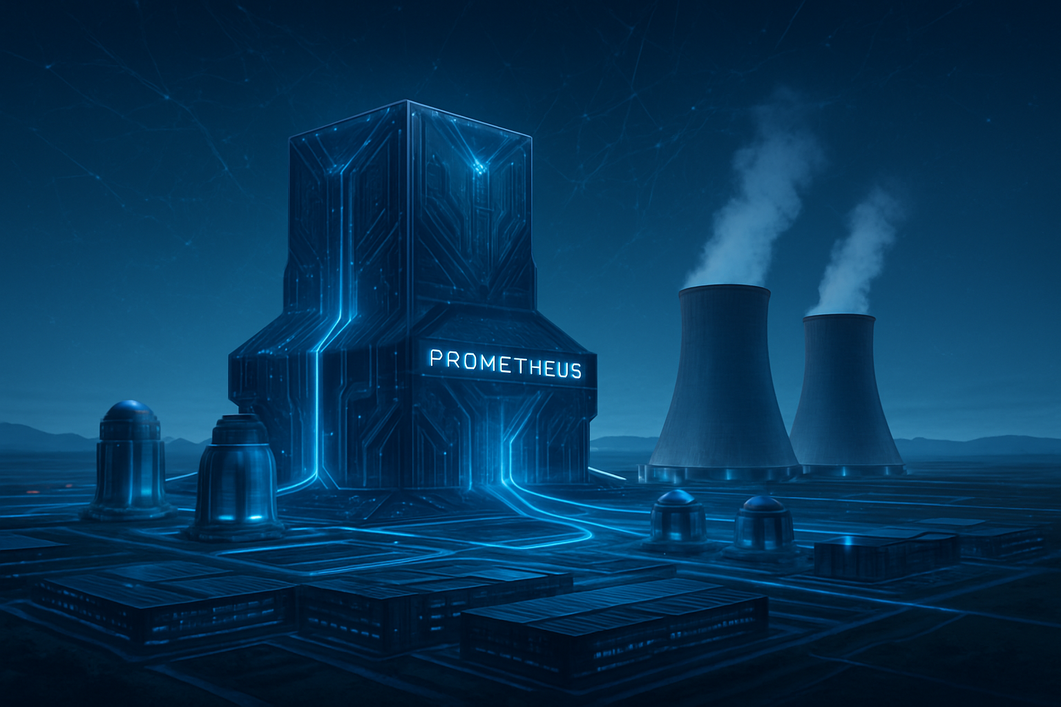
    The year 2026 has arrived as a definitive watershed moment for the global technology landscape, marking the transition of "Silicon Sovereignty" from a policy ambition to a physical reality. As of January 5, 2026, the United States has successfully re-shored a critical mass of advanced logic manufacturing, effectively ending a decades-long reliance on concentrated Asian supply chains. This shift is headlined by the commencement of high-volume manufacturing at Intel's state-of-the-art facilities in Arizona and the stabilization of TSMC’s domestic operations, signaling a new era where the world's most advanced AI hardware is once again "Made in America."

    The immediate significance of these developments cannot be overstated. For the first time in the modern era, the U.S. domestic supply chain is capable of producing sub-5nm chips at scale, providing a vital "Silicon Shield" against geopolitical volatility in the Taiwan Strait. While the road has been marred by strategic delays in the Midwest and shifting federal priorities, the operational status of the Southwest's "Silicon Desert" hubs confirms that the $52 billion bet placed by the CHIPS and Science Act is finally yielding its high-tech dividends.

    The Arizona Vanguard: 1.8nm and 4nm Realities

    The centerpiece of this manufacturing resurgence is Intel (NASDAQ: INTC) and its Fab 52 at the Ocotillo campus in Chandler, Arizona. As of early 2026, Fab 52 has officially transitioned into High-Volume Manufacturing (HVM) using the company’s ambitious 18A (1.8nm-class) process node. This technical achievement marks the first time a U.S.-based facility has surpassed the 2nm threshold, successfully integrating revolutionary RibbonFET gate-all-around transistors and PowerVia backside power delivery. Intel’s 18A node is currently powering the next generation of Panther Lake AI PC processors and Clearwater Forest server CPUs, with the fab ramping toward a target capacity of 40,000 wafer starts per month.

    Simultaneously, TSMC (NYSE: TSM) has silenced skeptics with the performance of its first Arizona facility, Fab 21. Initially plagued by labor disputes and cultural friction, the fab reached a staggering 92% yield rate for its 4nm (N4) process by the end of 2025—surpassing the yields of its comparable "mother fabs" in Taiwan. This operational efficiency has allowed TSMC to fulfill massive domestic orders for Apple (NASDAQ: AAPL) and Nvidia (NASDAQ: NVDA), ensuring that the silicon driving the world’s most advanced AI models and consumer devices is forged on American soil.

    However, the "Silicon Heartland" narrative has faced a reality check in the Midwest. Intel’s massive "Ohio One" complex in New Albany has seen its production timeline pushed back significantly. Originally slated for a 2025 opening, the facility is now expected to reach high-volume production no earlier than 2030. Intel has characterized this as a "strategic slowing" to align capital expenditures with a softening data center market and to navigate the transition to the "One Big Beautiful Bill Act" (OBBBA) of 2025, which restructured federal semiconductor incentives. Despite the delay, the Ohio site remains a cornerstone of the long-term U.S. strategy, currently serving as a massive shell project that represents a $28 billion commitment to future-proofing the domestic industry.

    Market Dynamics and the New Competitive Moat

    The successful ramp-up of domestic fabs has fundamentally altered the strategic positioning of the world’s largest tech giants. Companies like Nvidia and Apple, which previously faced "single-source" risks tied to Taiwan’s geopolitical status, now possess a diversified manufacturing base. This domestic capacity acts as a competitive moat, insulating these firms from potential export disruptions and the "Silicon Curtain" that has increasingly bifurcated the global market into Western and Eastern technological blocs.

    For Intel, the 2026 milestone is a make-or-break moment for its foundry services. By delivering 18A on schedule in Arizona, Intel is positioning itself as a viable alternative to TSMC for external customers seeking "sovereign-grade" silicon. Meanwhile, Samsung (KRX: 005930) is preparing to join the fray; its Taylor, Texas facility has pivoted exclusively to 2nm Gate-All-Around (GAA) technology. With mass production in Texas expected by late 2026, Samsung is already securing "anchor" AI clients like Tesla (NASDAQ: TSLA), further intensifying the competition for domestic manufacturing dominance.

    This re-shoring effort has also disrupted the traditional cost structures of the industry. Under the new policy frameworks of 2025 and 2026, "trusted" domestic silicon commands a market premium. The introduction of calibrated tariffs—including a 100% duty on Chinese-made semiconductors—has effectively neutralized the price advantage of overseas manufacturing for the U.S. market. This has forced startups and established AI labs alike to prioritize supply chain resilience over pure margin, leading to a surge in long-term domestic supply agreements.

    Geopolitics and the Silicon Shield

    The broader significance of the 2026 landscape lies in the concept of "Silicon Sovereignty." The U.S. government has moved away from the globalized efficiency models of the early 2000s, treating high-end semiconductors as a controlled strategic asset similar to enriched uranium. This "managed restriction" era is designed to ensure that the U.S. maintains a two-generation lead over adversarial nations. The Arizona and Texas hubs now provide a critical buffer; even in a worst-case scenario involving regional instability in Asia, the U.S. is on track to produce 20% of the world's leading-edge logic chips domestically by the end of the decade.

    This shift has also birthed massive public-private partnerships like "Project Stargate," a $500 billion initiative involving Oracle (NYSE: ORCL) and other major players to build hyper-scale AI data centers directly adjacent to these new power and manufacturing hubs. The first Stargate campus in Abilene, Texas, exemplifies the new American industrial model: a vertically integrated ecosystem where energy, silicon, and intelligence are co-located to minimize latency and maximize security.

    However, concerns remain regarding the "Silicon Curtain" and its impact on global innovation. The bifurcation of the market has led to redundant R&D costs and a fragmented standards environment. Critics argue that while the U.S. has secured its own supply, the resulting trade barriers could slow the overall pace of AI development by limiting the cross-pollination of hardware and software breakthroughs between East and West.

    The Horizon: 2nm and Beyond

    Looking toward the late 2020s, the focus is already shifting from 1.8nm to the sub-1nm frontier. The success of the Arizona fabs has set the stage for the next phase of the CHIPS Act, which will likely focus on advanced packaging and "glass substrate" technologies—the next bottleneck in AI chip performance. Experts predict that by 2028, the U.S. will not only lead in chip design but also in the complex assembly and testing processes that are currently concentrated in Southeast Asia.

    The next major challenge will be the workforce. While the facilities are now operational, the industry faces a projected shortfall of 50,000 specialized engineers by 2030. Addressing this "talent gap" through expanded immigration pathways for high-tech workers and domestic vocational programs will be the primary focus of the 2027 policy cycle. If the U.S. can solve the labor equation as successfully as it has the infrastructure equation, the "Silicon Heartland" may eventually span from the deserts of Arizona to the plains of Ohio.

    A New Chapter in Industrial History

    As we reflect on the state of the industry in early 2026, the progress is undeniable. The high-volume output at Intel’s Fab 52 and the high yields at TSMC’s Arizona facility represent a historic reversal of the offshoring trends that defined the last forty years. While the delays in Ohio serve as a reminder of the immense difficulty of building these "most complex machines on Earth," the momentum is clearly on the side of domestic manufacturing.

    The significance of this development in AI history is profound. We have moved from the era of "Software is eating the world" to "Silicon is the world." The ability to manufacture the physical substrate of intelligence domestically is the ultimate form of national security in the 21st century. In the coming months, industry watchers should look for the first 18A-based consumer products to hit the shelves and for Samsung’s Taylor facility to begin its final equipment move-in, signaling the completion of the first great wave of the American semiconductor renaissance.


    This content is intended for informational purposes only and represents analysis of current AI developments.

    TokenRing AI delivers enterprise-grade solutions for multi-agent AI workflow orchestration, AI-powered development tools, and seamless remote collaboration platforms.
    For more information, visit https://www.tokenring.ai/.
  • The Great Chill: How 1,800W GPUs Forced the Data Center Liquid Cooling Revolution of 2026

    The Great Chill: How 1,800W GPUs Forced the Data Center Liquid Cooling Revolution of 2026

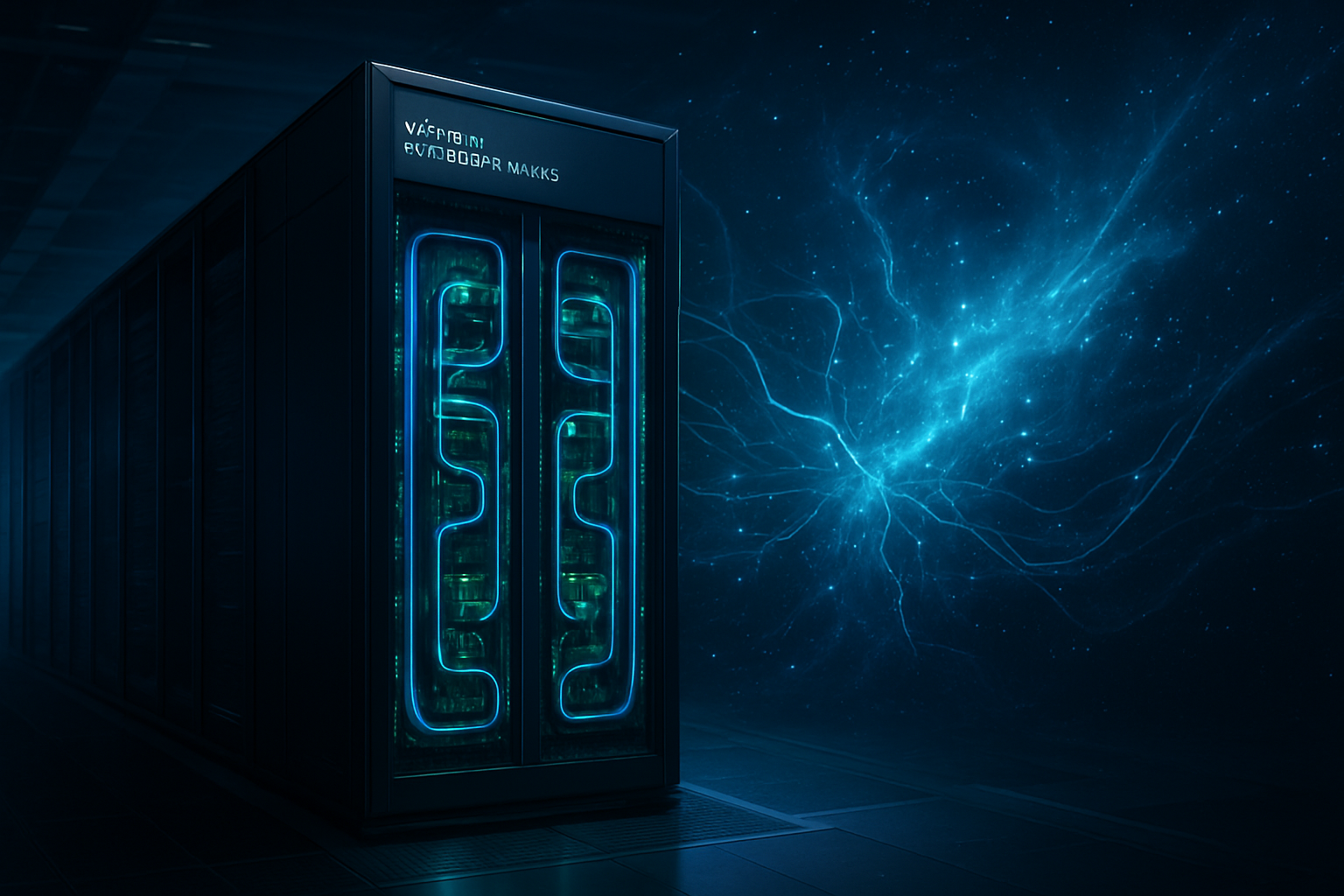
    The era of the "air-cooled" data center is officially coming to a close. As of January 2026, the artificial intelligence industry has hit a thermal wall that fans and air conditioning can no longer climb. Driven by the relentless power demands of next-generation silicon, the transition to liquid cooling has accelerated from a niche engineering choice to a global infrastructure mandate. Recent industry forecasts confirm that 38% of all data centers worldwide have now implemented liquid cooling solutions, a staggering jump from just 20% two years ago.

    This shift represents more than just a change in plumbing; it is a fundamental redesign of how the world’s digital intelligence is manufactured. As NVIDIA (NASDAQ: NVDA) begins the wide-scale rollout of its Rubin architecture, the power density of AI clusters has reached a point where traditional air cooling is physically incapable of removing heat fast enough to prevent chips from melting. The "AI Factory" has arrived, and it is running on a steady flow of coolant.

    The 1,000W Barrier and the Death of Air

    The primary catalyst for this infrastructure revolution is the skyrocketing Thermal Design Power (TDP) of modern AI accelerators. NVIDIA’s Blackwell Ultra (GB300) chips, which dominated the market through late 2025, pushed power envelopes to approximately 1,400W per GPU. However, the true "extinction event" for air cooling arrived with the 2026 debut of the Vera Rubin architecture. These chips are reaching a projected 1,800W per GPU, making them nearly twice as power-hungry as the flagship chips of the previous generation.

    At these power levels, the physics of air cooling simply break down. To cool a modern AI rack—which now draws between 250kW and 600kW—using air alone would require airflow velocities exceeding 15,000 cubic feet per minute. Industry experts describe this as "hurricane-force winds" inside a server room, creating noise levels and air turbulence that are physically damaging to equipment and impractical for human operators. Furthermore, air is an inefficient medium for heat transfer; liquid has nearly 4,000 times the heat-carrying capacity of air, allowing it to absorb and transport thermal energy from 1,800W chips with surgical precision.

    The industry has largely split into two technical camps: Direct-to-Chip (DTC) cold plates and immersion cooling. DTC remains the dominant choice, accounting for roughly 65-70% of the liquid cooling market in 2026. This method involves circulating coolant through metal plates directly attached to the GPU and CPU, allowing data centers to keep their existing rack formats while achieving a Power Usage Effectiveness (PUE) of 1.1. Meanwhile, immersion cooling—where entire servers are submerged in a non-conductive dielectric fluid—is gaining traction in the most extreme high-density tiers, offering a near-perfect PUE of 1.02 by eliminating fans entirely.

    The New Titans of Infrastructure

    The transition to liquid cooling has reshuffled the deck for hardware providers and infrastructure giants. Supermicro (NASDAQ: SMCI) has emerged as an early leader, currently claiming roughly 70% of the direct liquid cooling (DLC) market. By leveraging its "Data Center Building Block Solutions," the company has positioned itself to deliver fully integrated, liquid-cooled racks at a scale its competitors are still struggling to match, with revenue targets for fiscal year 2026 reaching as high as $40 billion.

    However, the "picks and shovels" of this revolution extend beyond the server manufacturers. Infrastructure specialists like Vertiv (NYSE: VRT) and Schneider Electric (EPA: SU) have become the "Silicon Sovereigns" of the 2026 economy. Vertiv has seen its valuation soar as it provides the mission-critical cooling loops and 800 VDC power portfolios required for 1-megawatt AI racks. Similarly, Schneider Electric’s strategic acquisition of Motivair in 2025 has allowed it to dominate the direct-to-chip portfolio, offering standardized reference designs that support the massive 132kW-per-rack requirements of NVIDIA’s latest clusters.

    For hyperscalers like Microsoft (NASDAQ: MSFT), Alphabet (NASDAQ: GOOGL), and Amazon (NASDAQ: AMZN), the adoption of liquid cooling is a strategic necessity. Those who can successfully manage the thermodynamics of these 2026-era "AI Factories" gain a significant competitive advantage in training larger models at a lower cost per token. The ability to pack more compute into a smaller physical footprint allows these giants to maximize the utility of their existing real estate, even as the power demands of their AI workloads continue to double every few months.

    Beyond Efficiency: The Rise of the AI Factory

    This transition marks a broader shift in the philosophy of data center design. NVIDIA CEO Jensen Huang has popularized the concept of the "AI Factory," where the data center is no longer viewed as a storage warehouse, but as an industrial plant that produces intelligence. In this paradigm, the primary unit of measure is no longer "uptime," but "tokens per second per watt." Liquid cooling is the essential lubricant for this industrial process, enabling the "gigawatt-scale" facilities that are now becoming the standard for frontier model training.

    The environmental implications of this shift are also profound. By reducing cooling energy consumption by 40% to 50%, liquid cooling is helping the industry manage the massive surge in total power demand. Furthermore, the high-grade waste heat captured by liquid systems is far easier to repurpose than the low-grade heat from air-cooled exhausts. In 2026, we are seeing the first wave of "circular" data centers that pipe their 60°C (140°F) waste heat directly into district heating systems or industrial processes, turning a cooling problem into a community asset.

    Despite these gains, the transition has not been without its challenges. The industry is currently grappling with a shortage of specialized plumbing components and a lack of standardized "quick-disconnect" fittings, which has led to some interoperability headaches. There are also lingering concerns regarding the long-term maintenance of immersion tanks and the potential for leaks in direct-to-chip systems. However, compared to the alternative—thermal throttling and the physical limits of air—these are seen as manageable engineering hurdles rather than deal-breakers.

    The Horizon: 2-Phase Cooling and 1MW Racks

    Looking ahead to the remainder of 2026 and into 2027, the industry is already eyeing the next evolution: two-phase liquid cooling. While current single-phase systems rely on the liquid staying in a liquid state, two-phase systems allow the coolant to boil and turn into vapor at the chip surface, absorbing massive amounts of latent heat. This technology is expected to be necessary as GPU power consumption moves toward the 2,000W mark.

    We are also seeing the emergence of modular, liquid-cooled "data centers in a box." These pre-fabricated units can be deployed in weeks rather than years, allowing companies to add AI capacity at the "edge" or in regions where traditional data center construction is too slow. Experts predict that by 2028, the concept of a "rack" may disappear entirely, replaced by integrated compute-cooling modules that resemble industrial engines more than traditional server cabinets.

    The most significant challenge on the horizon is the sheer scale of power delivery. While liquid cooling has solved the heat problem, the electrical grid must now keep up with the demand of 1-megawatt racks. We expect to see more data centers co-locating with nuclear power plants or investing in on-site small modular reactors (SMRs) to ensure a stable supply of the "fuel" their AI factories require.

    A Structural Shift in AI History

    The 2026 transition to liquid cooling will likely be remembered as a pivotal moment in the history of computing. It represents the point where AI hardware outpaced the traditional infrastructure of the 20th century, forcing a complete rethink of the physical environment required for digital thought. The 38% adoption rate we see today is just the beginning; by the end of the decade, an air-cooled AI server will likely be as rare as a vacuum tube.

    Key takeaways for the coming months include the performance of infrastructure stocks like Vertiv and Schneider Electric as they fulfill the massive backlog of cooling orders, and the operational success of the first wave of Rubin-based AI Factories. Investors and researchers should also watch for advancements in "coolant-to-grid" heat reuse projects, which could redefine the data center's role in the global energy ecosystem.

    As we move further into 2026, the message is clear: the future of AI is not just about smarter algorithms or bigger datasets—it is about the pipes, the pumps, and the fluid that keep the engines of intelligence running cool.


    This content is intended for informational purposes only and represents analysis of current AI developments.

    TokenRing AI delivers enterprise-grade solutions for multi-agent AI workflow orchestration, AI-powered development tools, and seamless remote collaboration platforms.
    For more information, visit https://www.tokenring.ai/.

  • The Silicon Sovereignty: Inside Samsung and Tesla’s $16.5 Billion Leap Toward Level 4 Autonomy

    The Silicon Sovereignty: Inside Samsung and Tesla’s $16.5 Billion Leap Toward Level 4 Autonomy

    In a move that has sent shockwaves through the global semiconductor and automotive sectors, Samsung Electronics (KRX: 005930) and Tesla, Inc. (NASDAQ: TSLA) have finalized a monumental $16.5 billion agreement to manufacture the next generation of Full Self-Driving (FSD) chips. This multi-year deal, officially running through 2033, positions Samsung as the primary architect for Tesla’s "AI6" hardware—the silicon brain designed to transition the world’s most valuable automaker from driver assistance to true Level 4 unsupervised autonomy.

    The partnership represents more than just a supply contract; it is a strategic realignment of the global tech supply chain. By leveraging Samsung’s cutting-edge 3nm and 2nm Gate-All-Around (GAA) transistor architecture, Tesla is securing the massive computational power required for its "world model" AI. For Samsung, the deal serves as a definitive validation of its foundry capabilities, proving that its domestic manufacturing in Taylor, Texas, can compete with the world’s most advanced fabrication facilities.

    The GAA Breakthrough: Scaling the 60% Yield Wall

    At the heart of this $16.5 billion deal is a significant technical triumph: Samsung’s stabilization of its 3nm GAA process. Unlike the traditional FinFET (Fin Field-Effect Transistor) technology used by competitors like TSMC (NYSE: TSM) for previous generations, GAA allows for more precise control over current flow, reducing power leakage and increasing efficiency. Reports from late 2025 indicate that Samsung has finally crossed the critical 60% yield threshold for its 3nm and 2nm-class nodes. This milestone is the industry-standard benchmark for profitable mass production, a figure that had eluded the company during the early, turbulent phases of its GAA rollout.

    The "AI6" chip, the centerpiece of this collaboration, is expected to deliver a staggering 1,500 to 2,000 TOPS (Tera Operations Per Second). This represents a tenfold increase in compute performance over the current Hardware 4.0 systems. To achieve this, Samsung is employing its SF2A automotive-grade process, which integrates a Backside Power Delivery Network (BSPDN). This innovation moves the power routing to the rear of the wafer, significantly reducing voltage drops and allowing the chip to maintain peak performance without draining the vehicle's battery—a crucial factor for maintaining electric vehicle (EV) range during intensive autonomous driving tasks.

    Industry experts have noted that Tesla engineers were reportedly given unprecedented access to "walk the line" at Samsung’s Taylor facility. This deep collaboration allowed Tesla to provide direct input on manufacturing optimizations, effectively co-engineering the production environment to suit the specific requirements of the AI6. This level of vertical integration is rare in the industry and highlights the shift toward custom silicon as the primary differentiator in the automotive race.

    Shifting the Foundry Balance: Samsung’s Strategic Coup

    This deal marks a pivotal shift in the ongoing "foundry wars." For years, TSMC has held a dominant grip on the high-end semiconductor market, serving as the sole manufacturer for many of the world’s most advanced chips. However, Tesla’s decision to move its most critical future hardware back to Samsung signals a desire to diversify its supply chain and mitigate the geopolitical risks associated with concentrated production in Taiwan. By utilizing the Taylor, Texas foundry, Tesla is creating a "domestic" silicon pipeline, located just miles from its Austin Gigafactory, which aligns perfectly with the incentives of the U.S. CHIPS Act.

    For Samsung, securing Tesla as an anchor client for its 2nm GAA process is a major blow to TSMC’s perceived invincibility. It proves that Samsung’s bet on GAA architecture—a technology TSMC is only now transitioning toward for its 2nm nodes—has paid off. This successful partnership is already attracting interest from other Western "hyperscalers" like Qualcomm and AMD, who are looking for viable alternatives to TSMC’s capacity constraints. The $16.5 billion figure is seen by many as a floor; with Tesla’s plans for robotaxis and the Optimus humanoid robot, the total value of the partnership could eventually exceed $50 billion.

    The competitive implications extend beyond the foundries to the chip designers themselves. By developing its own custom AI6 silicon with Samsung, Tesla is effectively bypassing traditional automotive chip suppliers. This move places immense pressure on companies like NVIDIA (NASDAQ: NVDA) and Mobileye to prove that their off-the-shelf autonomous solutions can compete with the hyper-optimized, vertically integrated stack that Tesla is building.

    The Era of the Software-Defined Vehicle and Level 4 Autonomy

    The Samsung-Tesla deal is a clear indicator that the automotive industry has entered the era of the "Software-Defined Vehicle" (SDV). In this new paradigm, the value of a car is determined less by its mechanical components and more by its digital capabilities. The AI6 chip provides the necessary "headroom" for Tesla to move away from dozens of small Electronic Control Units (ECUs) toward a centralized zonal architecture. This centralization allows a single powerful chip to control everything from powertrain management to infotainment and, most importantly, the complex neural networks required for Level 4 autonomy.

    Level 4 autonomy—defined as the vehicle's ability to operate without human intervention in specific conditions—requires the car to run a "world model" in real-time. This involves simulating and predicting the movements of every object in a 360-degree field of vision simultaneously. The massive compute power provided by Samsung’s 3nm and 2nm GAA chips is the only way to process this data with the low latency required for safety. This milestone mirrors previous AI breakthroughs, such as the transition from CPU to GPU training for Large Language Models, where a hardware leap enabled a fundamental shift in software capability.

    However, this transition is not without concerns. The increasing reliance on a single, highly complex chip raises questions about system redundancy and cybersecurity. If the "brain" of the car is compromised or suffers a hardware failure, the implications for a Level 4 vehicle are far more severe than in traditional cars. Furthermore, the environmental impact of manufacturing such advanced silicon remains a topic of debate, though the efficiency gains of the GAA architecture are intended to offset some of the energy demands of the AI itself.

    Future Horizons: From Robotaxis to Humanoid Robots

    Looking ahead, the implications of the AI6 chip extend far beyond the passenger car. Tesla has already indicated that the architecture of the AI6 will serve as the foundation for the "Optimus" Gen 3 humanoid robot. The spatial awareness, path planning, and object recognition required for a robot to navigate a human home or factory are nearly identical to the challenges faced by a self-driving car. This cross-platform utility ensures that the $16.5 billion investment will yield dividends across multiple industries.

    In the near term, we can expect the first AI6-equipped vehicles to begin rolling off the assembly line in late 2026 or early 2027. These vehicles will likely serve as the vanguard for Tesla’s long-promised robotaxi fleet. The challenge remains in the regulatory environment, as hardware capability often outpaces legal frameworks. Experts predict that as the safety data from these next-gen chips begins to accumulate, the pressure on regulators to approve unsupervised autonomous driving will become irresistible.

    A New Chapter in AI History

    The $16.5 billion deal between Samsung and Tesla is a watershed moment in the history of artificial intelligence and transportation. It represents the successful marriage of advanced semiconductor manufacturing and frontier AI software. By successfully scaling the 3nm GAA process and reaching a 60% yield, Samsung has not only saved its foundry business but has also provided the hardware foundation for the next great leap in mobility.

    As we move into 2026, the industry will be watching closely to see how quickly the Taylor facility can scale to meet Tesla’s insatiable demand. This partnership has set a new standard for how tech giants and automakers must collaborate to survive in an AI-driven world. The "Silicon Sovereignty" of the future will belong to those who can control the entire stack—from the gate of the transistor to the code of the autonomous drive.


    This content is intended for informational purposes only and represents analysis of current AI developments.

    TokenRing AI delivers enterprise-grade solutions for multi-agent AI workflow orchestration, AI-powered development tools, and seamless remote collaboration platforms.
    For more information, visit https://www.tokenring.ai/.

  • The Power Flip: How Backside Delivery is Rescuing the 1,000W AI Era

    The Power Flip: How Backside Delivery is Rescuing the 1,000W AI Era

    The semiconductor industry has officially entered the "Angstrom Era," marked by the most radical architectural shift in chip manufacturing in over three decades. As of January 5, 2026, the traditional method of routing power through the front of a silicon wafer—a practice that has persisted since the dawn of the integrated circuit—is being abandoned in favor of Backside Power Delivery Networks (BSPDN). This transition is not merely an incremental improvement; it is a fundamental necessity driven by the insatiable energy demands of generative AI and the physical limitations of atomic-scale transistors.

    The immediate significance of this shift was underscored today at CES 2026, where Intel Corporation (Nasdaq:INTC) announced the broad market availability of its "Panther Lake" processors, the first consumer-grade chips to utilize high-volume backside power. By decoupling the power delivery from the signal routing, chipmakers are finally solving the "wiring bottleneck" that has plagued the industry. This development ensures that the next generation of AI accelerators, which are now pushing toward 1,000W to 1,500W per module, can receive stable electricity without the catastrophic voltage losses that would have rendered them inefficient or unworkable on older architectures.

    The Technical Divorce: PowerVia vs. Super Power Rail

    At the heart of this revolution are two competing technical philosophies: Intel’s PowerVia and Taiwan Semiconductor Manufacturing Company’s (NYSE:TSM) Super Power Rail. Historically, both power and data signals were routed through a complex "jungle" of metal layers on top of the transistors. As transistors shrunk to the 2nm and 1.8nm levels, these wires became so thin and crowded that resistance skyrocketed, leading to significant "IR drop"—a phenomenon where voltage decreases as it travels through the chip. BSPDN solves this by moving the power delivery to the reverse side of the wafer, effectively giving the chip two "fronts": one for data and one for energy.

    Intel’s PowerVia, debuting in the 18A (1.8nm) process node, utilizes a "nano-TSV" (Through Silicon Via) approach. In this implementation, Intel builds the transistors first, then flips the wafer to create small vertical connections that bridge the backside power layers to the metal layers on the front. This method is considered more manufacturable and has allowed Intel to claim a first-to-market advantage. Early data from Panther Lake production indicates a 30% improvement in voltage droop and a 6% frequency boost at identical power levels compared to traditional front-side delivery. Furthermore, by clearing the "congestion" on the front side, Intel has achieved a staggering 90% standard cell utilization, drastically increasing logic density.

    TSMC is taking a more aggressive, albeit delayed, approach with its A16 (1.6nm) node and its "Super Power Rail" technology. Unlike Intel’s nano-TSVs, TSMC’s implementation connects the backside power network directly to the source and drain of the transistors. This direct-contact method is significantly more complex to manufacture, requiring advanced material science to prevent contamination during the bonding process. However, the theoretical payoff is higher: TSMC targets an 8–10% speed improvement and up to a 20% power reduction. While Intel is shipping products today, TSMC is positioning its Super Power Rail as the "refined" version of BSPDN, slated for mass production in the second half of 2026 to power the next generation of high-end AI and mobile silicon.

    Strategic Dominance and the AI Arms Race

    The shift to backside power has created a new competitive landscape for tech giants and specialized AI labs. Intel’s early lead with 18A and PowerVia is a strategic masterstroke for its Foundry business. By proving the viability of BSPDN in high-volume consumer chips like Panther Lake, Intel is signaling to major fabless customers that it has solved the most difficult scaling challenge of the decade. This puts immense pressure on Samsung Electronics (KRX:005930), which is also racing to implement its own BSPDN version to remain competitive in the logic foundry market.

    For AI powerhouses like NVIDIA (Nasdaq:NVDA), the arrival of BSPDN is a lifeline. NVIDIA’s current "Blackwell" architecture and the upcoming "Rubin" platform (scheduled for late 2026) are pushing the limits of data center power infrastructure. With GPUs now drawing well over 1,000W, traditional power delivery would result in massive heat generation and energy waste. By adopting TSMC’s A16 process and Super Power Rail, NVIDIA can ensure that its future Rubin GPUs maintain high clock speeds and reliability even under the extreme workloads required for training trillion-parameter models.

    The primary beneficiaries of this development are the "Magnificent Seven" and other hyperscalers who operate massive data centers. Companies like Apple (Nasdaq:AAPL) and Alphabet (Nasdaq:GOOGL) are already reportedly in the queue for TSMC’s A16 capacity. The ability to pack more compute into the same thermal envelope allows these companies to maximize their return on investment for AI infrastructure. Conversely, startups that cannot secure early access to these advanced nodes may find themselves at a performance-per-watt disadvantage, potentially widening the gap between the industry leaders and the rest of the field.

    Solving the 1,000W Crisis in the AI Landscape

    The broader significance of BSPDN lies in its role as a "force multiplier" for AI scaling laws. For years, experts have worried that we would hit a "power wall" where the energy required to drive a chip would exceed its ability to dissipate heat. BSPDN effectively moves that wall. By thinning the silicon wafer to allow for backside connections, chipmakers also improve the thermal path from the transistors to the cooling solution. This is critical for the 1,000W+ power demands of modern AI accelerators, which would otherwise face severe thermal throttling.

    This architectural change mirrors previous industry milestones, such as the transition from planar transistors to FinFETs in the early 2010s. Just as FinFETs allowed the industry to continue scaling despite leakage current issues, BSPDN allows scaling to continue despite resistance issues. However, the transition is not without concerns. The manufacturing process for BSPDN is incredibly delicate; it involves bonding two wafers together with nanometer precision and then grinding one down to a thickness of just a few hundred nanometers. Any misalignment can result in total wafer loss, making yield management the primary challenge for 2026.

    Moreover, the environmental impact of this technology is a double-edged sword. While BSPDN makes chips more efficient on a per-calculation basis, the sheer performance gains it enables are likely to encourage even larger, more power-hungry AI clusters. As the industry moves toward 600kW racks for data centers, the efficiency gains of backside power will be essential just to keep the lights on, though they may not necessarily reduce the total global energy footprint of AI.

    The Horizon: Beyond 1.6 Nanometers

    Looking ahead, the successful deployment of PowerVia and Super Power Rail sets the stage for the sub-1nm era. Industry experts predict that the next logical step after BSPDN will be the integration of "optical interconnects" directly onto the backside of the die. Once the power delivery has been moved to the rear, the front side is theoretically "open" for even more dense signal routing, including light-based data transmission that could eliminate traditional copper wiring altogether for long-range on-chip communication.

    In the near term, the focus will shift to how these technologies handle the "Rubin" generation of GPUs and the "Panther Lake" successor, "Nova Lake." The challenge remains the cost: the complexity of backside power adds significant steps to the lithography process, which will likely keep the price of advanced AI silicon high. Analysts expect that by 2027, BSPDN will be the standard for all high-performance computing (HPC) chips, while budget-oriented mobile chips may stick to traditional front-side delivery for another generation to save on manufacturing costs.

    A New Foundation for Silicon

    The arrival of Backside Power Delivery marks a pivotal moment in the history of computing. It represents a "flipping of the script" in how we design and build the brains of our digital world. By physically separating the two most critical components of a chip—its energy and its information—engineers have unlocked a new path for Moore’s Law to continue into the Angstrom Era.

    The key takeaways from this transition are clear: Intel has successfully reclaimed a technical lead by being the first to market with PowerVia, while TSMC is betting on a more complex, higher-performance implementation to maintain its dominance in the AI accelerator market. As we move through 2026, the industry will be watching yield rates and the performance of NVIDIA’s next-generation chips to see which approach yields the best results. For now, the "Power Flip" has successfully averted a scaling crisis, ensuring that the next wave of AI breakthroughs will have the energy they need to come to life.


    This content is intended for informational purposes only and represents analysis of current AI developments.

    TokenRing AI delivers enterprise-grade solutions for multi-agent AI workflow orchestration, AI-powered development tools, and seamless remote collaboration platforms.
    For more information, visit https://www.tokenring.ai/.

  • The Angstrom Era Begins: ASML’s High-NA EUV and the $380 Million Bet to Save Moore’s Law

    The Angstrom Era Begins: ASML’s High-NA EUV and the $380 Million Bet to Save Moore’s Law

    As of January 5, 2026, the semiconductor industry has officially entered the "Angstrom Era," a transition marked by the high-volume deployment of the most complex machine ever built: the High-Numerical Aperture (High-NA) Extreme Ultraviolet (EUV) lithography scanner. Developed by ASML (NASDAQ: ASML), the Twinscan EXE:5200B has become the defining tool for the sub-2nm generation of chips. This technological leap is not merely an incremental upgrade; it is the gatekeeper for the next decade of Moore’s Law, providing the precision necessary to print transistors at scales where atoms are the primary unit of measurement.

    The immediate significance of this development lies in the radical shift of the competitive landscape. Intel (NASDAQ: INTC), after a decade of trailing its rivals, has seized the "first-mover" advantage by becoming the first to integrate High-NA into its production lines. This aggressive stance is aimed directly at reclaiming the process leadership crown from TSMC (NYSE: TSM), which has opted for a more conservative, cost-optimized approach. As AI workloads demand exponentially more compute density and power efficiency, the success of High-NA EUV will dictate which silicon giants will power the next generation of generative AI models and hyperscale data centers.

    The Twinscan EXE:5200B: Engineering the Sub-2nm Frontier

    The technical specifications of the Twinscan EXE:5200B represent a paradigm shift in lithography. The "High-NA" designation refers to the increase in numerical aperture from 0.33 in standard EUV machines to 0.55. This change allows the machine to achieve a staggering 8nm resolution, enabling the printing of features approximately 1.7 times smaller than previous tools. In practical terms, this translates to a 2.9x increase in transistor density, allowing engineers to cram billions more gates onto a single piece of silicon without the need for the complex "multi-patterning" techniques that have plagued 3nm and 2nm yields.

    Beyond resolution, the EXE:5200B addresses the two most significant hurdles of early High-NA prototypes: throughput and alignment. The production-ready model now achieves a throughput of 175 to 200 wafers per hour (wph), matching the productivity of the latest low-NA scanners. Furthermore, it boasts an overlay accuracy of 0.7nm. This sub-nanometer precision is critical for a process known as "field stitching." Because High-NA optics halve the exposure field size, larger chips—such as the massive GPUs produced by NVIDIA (NASDAQ: NVDA)—must be printed in two separate halves. The 0.7nm overlay ensures these halves are aligned with such perfection that they function as a single, seamless monolithic die.

    This approach differs fundamentally from the industry's previous trajectory. For the past five years, foundries have relied on "multi-patterning," where a single layer is printed using multiple exposures to achieve finer detail. While effective, multi-patterning increases the risk of defects and significantly lengthens the manufacturing cycle. High-NA EUV returns the industry to "single-patterning" for the most critical layers, drastically simplifying the manufacturing flow and improving the "time-to-market" for cutting-edge designs. Initial reactions from the research community suggest that while the $380 million price tag per machine is daunting, the reduction in process steps and the jump in density make it an inevitable necessity for the sub-2nm era.

    A Tale of Two Strategies: Intel’s Leap vs. TSMC’s Caution

    The deployment of High-NA EUV has created a strategic schism between the world’s leading chipmakers. Intel has positioned itself as the "High-NA Vanguard," utilizing the EXE:5200B to underpin its 18A (1.8nm) and 14A (1.4nm) nodes. By early 2026, Intel's 18A process has reached high-volume manufacturing, with the first "Panther Lake" consumer chips hitting shelves. While 18A was designed to be compatible with standard EUV, Intel is selectively using High-NA tools to "de-risk" the technology before its 14A node becomes "High-NA native" later this year. This early adoption is a calculated risk to prove to foundry customers that Intel Foundry is once again the world's most advanced manufacturer.

    Conversely, TSMC has maintained a "wait-and-see" approach, focusing on optimizing its existing low-NA EUV infrastructure for its A14 (1.4nm) node. TSMC’s leadership has argued that the current cost-per-wafer for High-NA is too high for mass-market mobile chips, preferring to use multi-patterning on its ultra-mature NXE:3800E scanners. This creates a fascinating market dynamic: Intel is betting on technical superiority and process simplification to attract high-margin AI customers, while TSMC is betting on cost-efficiency and yield stability.

    The implications for the broader market are profound. If Intel successfully scales 14A using the EXE:5200B, it could potentially offer AI companies like AMD (NASDAQ: AMD) and even NVIDIA a performance-per-watt advantage that TSMC cannot match until its own High-NA transition, currently slated for 2027 or 2028. This disruption could shift the balance of power in the foundry business, which TSMC has dominated for over a decade. Startups specializing in "AI-first" silicon also stand to benefit, as the single-patterning capability of High-NA reduces the "design-to-chip" lead time, allowing for faster iteration of specialized neural processing units (NPUs).

    The Silicon Gatekeeper of the AI Revolution

    The significance of ASML’s High-NA dominance extends far beyond corporate rivalry; it is the physical foundation of the AI revolution. Modern Large Language Models (LLMs) are currently constrained by two factors: the amount of high-speed memory that can be placed near the compute units and the power efficiency of the data center. Sub-2nm chips produced with the EXE:5200B are expected to consume 25% to 35% less power for the same frequency compared to 3nm equivalents. In an era where electricity and cooling costs are the primary bottlenecks for AI scaling, these efficiency gains are worth billions to hyperscalers like Microsoft (NASDAQ: MSFT) and Google (NASDAQ: GOOGL).

    Furthermore, the transition to High-NA mirrors previous industry milestones, such as the initial shift from DUV to EUV in 2019. Just as that transition enabled the 5nm and 3nm chips that power today’s smartphones and AI accelerators, High-NA is the "second act" of EUV that will carry the industry toward the 1nm mark. However, the stakes are higher now. The geopolitical importance of semiconductor leadership has never been greater, and the "High-NA club" is currently an exclusive group. With ASML being the sole provider of these machines, the global supply chain for the most advanced AI hardware now runs through a single point of failure in Veldhoven, Netherlands.

    Potential concerns remain regarding the "halved field" issue. While field stitching has been proven in the lab, doing it at a scale of millions of units per month without impacting yield is a monumental challenge. If the stitching process leads to higher defect rates, the cost of the world’s most advanced AI GPUs could skyrocket, potentially slowing the democratization of AI compute. Nevertheless, the industry has historically overcome such lithographic hurdles, and the consensus is that High-NA is the only viable path forward.

    The Road to 14A and Beyond

    Looking ahead, the next 24 months will be critical for the validation of High-NA technology. Intel is expected to release its 14A Process Design Kit (PDK 1.0) to foundry customers in the coming months, which will be the first design environment built entirely around the capabilities of the EXE:5200B. This node will introduce "PowerDirect," a second-generation backside power delivery system that, when combined with High-NA lithography, promises a 20% performance boost over the already impressive 18A node.

    Experts predict that by 2028, the "High-NA gap" between Intel and TSMC will close as the latter finally integrates the tools into its "A14P" process. However, the "learning curve" advantage Intel is building today could prove difficult to overcome. We are also likely to see the emergence of "Hyper-NA" research—tools with numerical apertures even higher than 0.55—as the industry begins to look toward the sub-10-angstrom (sub-1nm) era in the 2030s. The immediate challenge for ASML and its partners will be to drive down the cost of these machines and improve the longevity of the specialized photoresists and masks required for such extreme resolutions.

    A New Chapter in Computing History

    The deployment of the ASML Twinscan EXE:5200B marks a definitive turning point in the history of computing. By enabling the mass production of sub-2nm chips, ASML has effectively extended the life of Moore’s Law at a time when many predicted its demise. Intel’s aggressive adoption of this technology represents a "moonshot" attempt to regain its former glory, while the industry’s shift toward "Angstrom-class" silicon provides the necessary hardware runway for the next decade of AI innovation.

    The key takeaways are clear: the EXE:5200B is the most productive and precise lithography tool ever created, Intel is currently the only player using it for high-volume manufacturing, and the future of AI hardware is now inextricably linked to the success of High-NA EUV. In the coming weeks and months, all eyes will be on Intel’s 18A yield reports and the first customer tape-outs for the 14A node. These metrics will serve as the first real-world evidence of whether the High-NA era will deliver on its promise of a new golden age for silicon.


    This content is intended for informational purposes only and represents analysis of current AI developments.

    TokenRing AI delivers enterprise-grade solutions for multi-agent AI workflow orchestration, AI-powered development tools, and seamless remote collaboration platforms.
    For more information, visit https://www.tokenring.ai/.