As of February 5, 2026, the global race for Artificial General Intelligence (AGI) has moved out of the laboratory and into the realm of heavy industry. Project Stargate, the unprecedented $500 billion supercomputing initiative led by OpenAI in partnership with Microsoft (NASDAQ: MSFT) and Oracle (NYSE: ORCL), has officially transitioned from a series of ambitious blueprints into the largest private-sector infrastructure project in human history. Formally inaugurated in early 2025 at a landmark White House summit, the project aims to secure American technological hegemony through a massive expansion of domestic compute capacity, treating AI development not merely as a corporate milestone, but as a critical pillar of national security.
The initiative represents a fundamental shift in how the world’s most powerful AI models are built and deployed. By moving toward a "steel in the ground" strategy, the consortium is attempting to solve the primary bottleneck of the AI era: the physical limits of power, space, and silicon. With a roadmap designed to reach 10 gigawatts of power capacity by 2029, Project Stargate is currently reshaping the American landscape, turning rural regions in Texas and Ohio into the high-tech nerve centers of the 21st century.
The Architect of AGI: 2 Million Chips and 10 Gigawatts of Power
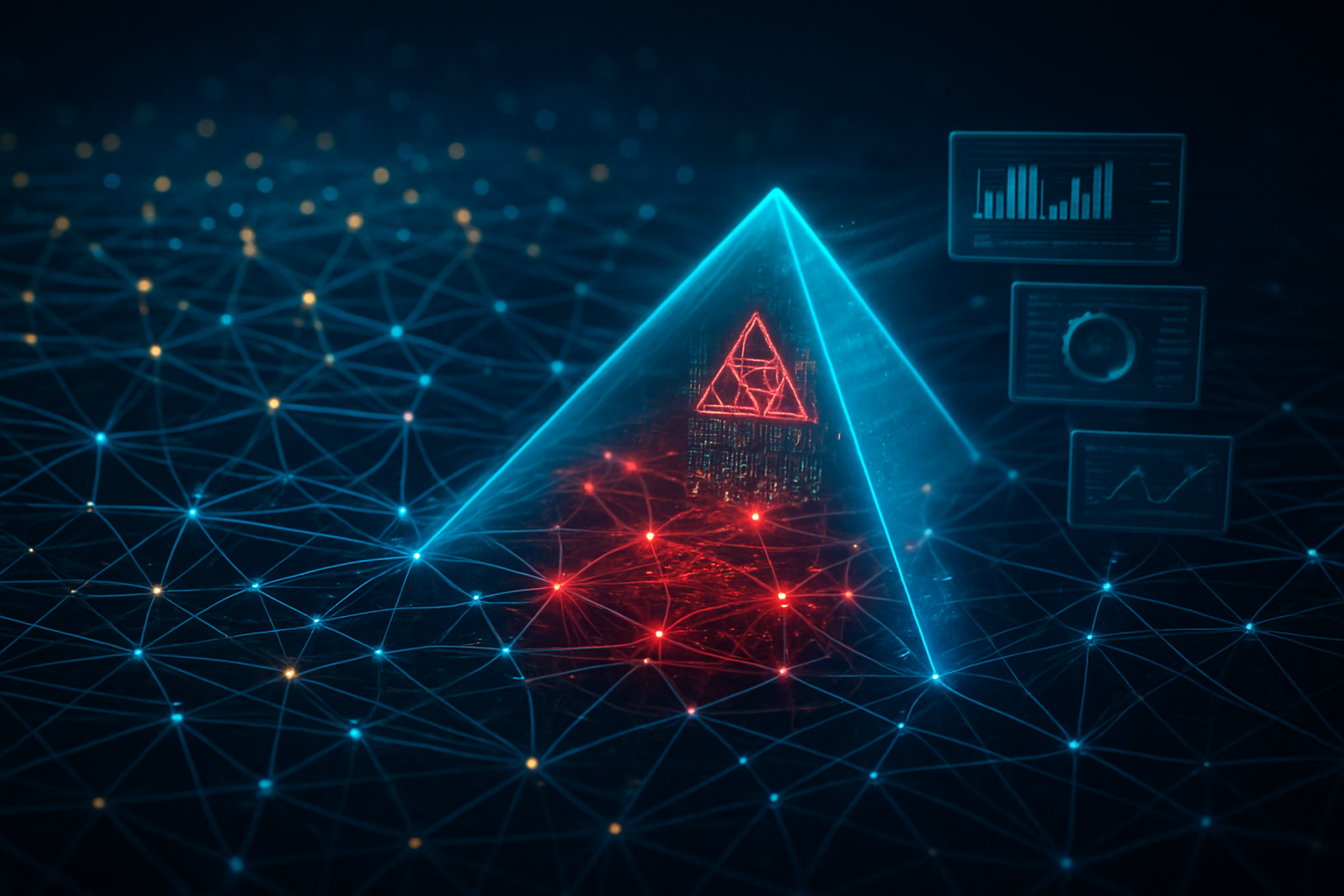
At the heart of Project Stargate lies a technical ambition that dwarfs any previous computing endeavor. The initiative is currently building a network of 20 "colossal" data centers across the United States, each spanning approximately 500,000 square feet. The flagship site, "Stargate I" in Abilene, Texas, became operational late last year and is already serving as the training ground for the next generation of OpenAI’s frontier models. Technical specifications reveal that the infrastructure is designed to house over 2 million AI chips, primarily utilizing NVIDIA (NASDAQ: NVDA) GB200 Blackwell architecture and specialized "Zettascale" clusters provided by Oracle.
What sets Stargate apart from previous data center projects is its hyper-dense interconnectivity. Oracle has deployed advanced networking technology that allows for the clustering of up to 800,000 GPUs within a strict two-kilometer radius to maintain the low-latency requirements of large-scale model training. Furthermore, the project is tackling the energy crisis head-on by exploring the integration of Small Modular Reactors (SMRs) to provide dedicated, carbon-neutral power to its sites. This move towards energy independence is a significant departure from the traditional model of relying on local municipal grids, which have struggled to keep pace with the massive 10-gigawatt demand—enough energy to power roughly 7.5 million homes.
Initial reactions from the AI research community have been a mix of awe and trepidation. Leading researchers at MIT and Stanford have noted that the sheer scale of Stargate could enable the training of models with parameters in the quadrillions, potentially leading to breakthroughs in reasoning and scientific discovery that were previously thought to be decades away. However, industry experts also warn that the centralization of such massive compute power creates a "compute moat" that may be impossible for smaller labs or academic institutions to cross, effectively bifurcating the AI research world into those with Stargate access and those without.
A New Corporate Hierarchy: Oracle, Microsoft, and the Shift in AI Dominance
The financial and strategic structure of Project Stargate has significantly altered the power dynamics among Silicon Valley’s elite. While Microsoft remains a primary technology partner and a major stakeholder in OpenAI, Project Stargate represents a pivot toward infrastructure diversification. Under the current arrangement, OpenAI has expanded its horizons beyond Microsoft's Azure, tapping Oracle to provide the "physical backbone" of the new supercomputing clusters. Oracle’s involvement has been transformative for the company, which has committed over $150 billion in capital expenditure to the project, positioning itself as the premier provider of "sovereign AI" infrastructure.
This shift has created a unique competitive landscape. Microsoft continues to hold rights of first refusal and exclusive API access to OpenAI's models, but the physical ownership of the hardware is now shared among a broader consortium that includes SoftBank (TYO: 9984) and the Abu Dhabi-backed MGX. This "Stargate LLC" structure allows OpenAI to scale at a pace that would be balance-sheet prohibitive for any single corporation. For tech giants like Google (NASDAQ: GOOGL) and Meta (NASDAQ: META), the $500 billion scale of Stargate raises the stakes of the AI arms race to an astronomical level, forcing a re-evaluation of their own infrastructure investments to avoid being left behind in the AGI pursuit.
Startups and mid-tier AI companies are feeling the disruption most acutely. As Oracle and Microsoft prioritize the massive compute needs of the Stargate initiative, the cost of high-end GPU clusters for smaller players has remained volatile. However, some analysts argue that the massive expansion of infrastructure will eventually lead to a "trickle-down" of compute availability as older hardware is cycled out of the Stargate sites. In the near term, the strategic advantage lies squarely with the consortium, which now controls the most concentrated collection of AI processing power on the planet.
The Manhattan Project of the 2020s: National Security and Global Competition
Project Stargate is frequently referred to in Washington as the "Manhattan Project for AI," a comparison that underscores its status as a matter of national survival. The White House and the Department of Defense have increasingly framed the project as a strategic deterrent against adversaries. By centralizing $500 billion of investment into U.S.-based AI infrastructure, the administration aims to ensure that the "intelligence age" remains anchored in American values and oversight. This framing has led to unprecedented government support, including the use of emergency declarations to bypass traditional permitting hurdles for electrical grid expansions and data center construction.
The wider significance of this project extends beyond military application; it is viewed as a tool for economic re-industrialization. The initiative is projected to create between 100,000 and 250,000 jobs across the American Midwest and Southwest, revitalizing regions through "AI-corridor" developments. Comparisons to the Apollo program or the Interstate Highway System are common, as the project necessitates a fundamental upgrade of the nation's energy and telecommunications networks. This integration of private capital and national interest marks a new era of industrial policy, where the line between a private tech company and a national utility becomes increasingly blurred.
However, the scale of Stargate also invites significant concerns. Environmental advocates point to the staggering water and electricity requirements of the data centers, while civil liberty groups have raised alarms about the potential for such a massive "intelligence engine" to be used for state surveillance. Furthermore, the reliance on international funding from entities like SoftBank and MGX has sparked debates in Congress regarding the "sovereignty" of American AI, leading to strict protocols on data residency and hardware security within the Stargate sites.
The Road Ahead: From Supercomputers to Autonomous Systems
Looking toward the future, the completion of the 10-gigawatt capacity target by 2029 is just the beginning. Experts predict that the massive compute pool provided by Project Stargate will serve as the "operating system" for a new era of autonomous systems, from self-navigating logistics networks to AI-driven drug discovery platforms. Near-term developments are expected to focus on "Stargate II," a planned expansion that could incorporate even more experimental cooling technologies and perhaps the first dedicated AI-optimizing chipsets designed in-house by the consortium members.
The challenges that remain are largely logistical and political. Managing the sheer heat output of 2 million chips and securing the supply chain for specialized components like high-bandwidth memory (HBM) will require constant innovation. Additionally, as the project nears its goal of AGI-level capabilities, the debate over AI safety and alignment will likely move from the halls of academia into the halls of government, with Stargate serving as the primary testbed for new regulatory frameworks. Predictably, the next 24 months will be defined by the "race to the first light"—the moment when the fully integrated Stargate I cluster begins training its first trillion-parameter model.
Conclusion: A Turning Point in Human History
Project Stargate stands as a testament to the belief that the future belongs to those who control the most intelligence. With its $500 billion price tag and its status as a national security priority, the initiative has elevated AI from a software trend to a foundational element of national infrastructure. The partnership between OpenAI, Microsoft, and Oracle has successfully bridged the gap between silicon and steel, creating a physical manifestation of the digital revolution that is visible across the American landscape.
The key takeaway for 2026 is that the era of "small AI" is over. We have entered a period of massive, centralized compute that functions more like a power utility than a traditional tech service. As the Stargate sites in Texas and Ohio continue to come online, the world will be watching to see if this unprecedented concentration of power leads to the promised breakthroughs in human capability or to new, unforeseen challenges. In the coming months, keep a close eye on the rollout of the project’s SMR energy pilots and the first outputs from the Abilene cluster, as these will be the true indicators of whether Stargate can live up to its name and open a new door for humanity.
This content is intended for informational purposes only and represents analysis of current AI developments.
TokenRing AI delivers enterprise-grade solutions for multi-agent AI workflow orchestration, AI-powered development tools, and seamless remote collaboration platforms.
For more information, visit https://www.tokenring.ai/.