Blog

  • The Great Decoupling: NVIDIA’s Data Center Revenue Now Six Times Larger Than Intel and AMD Combined

    The Great Decoupling: NVIDIA’s Data Center Revenue Now Six Times Larger Than Intel and AMD Combined

    As of January 8, 2026, the global semiconductor landscape has reached a definitive tipping point, marking the end of the "CPU-first" era that defined computing for nearly half a century. Recent financial disclosures for the final quarters of 2025 have revealed a staggering reality: NVIDIA (NASDAQ: NVDA) now generates more revenue from its data center segment alone than the combined data center and CPU revenues of its two largest historical rivals, Intel (NASDAQ: INTC) and AMD (NASDAQ: AMD). This financial chasm—with NVIDIA’s $51.2 billion in quarterly data center revenue dwarfing the $8.4 billion combined total of its competitors—signals a permanent shift in the industry’s center of gravity toward accelerated computing.

    The disparity is even more pronounced when isolating for general-purpose CPUs. Analysts estimate that NVIDIA's data center revenue is now approximately eight times the combined server CPU revenue of Intel and AMD. This "Great Decoupling" highlights a fundamental change in how the world’s most powerful computers are built. No longer are GPUs merely "accelerators" added to a CPU-based system; in the modern "AI Factory," the GPU is the primary compute engine, and the CPU has been relegated to a supporting role, managing housekeeping tasks while NVIDIA’s Blackwell architecture performs the heavy lifting of modern intelligence.

    The Blackwell Era and the Rise of the Integrated Platform

    The primary catalyst for this financial explosion has been the unprecedented ramp-up of NVIDIA’s Blackwell architecture. Throughout 2025, the B200 and GB200 chips became the most sought-after commodities in the tech world. Unlike previous generations where chips were sold individually, NVIDIA’s dominance in 2025 was driven by the sale of entire integrated systems, such as the NVL72 rack. These systems combine 72 Blackwell GPUs with NVIDIA’s own Grace CPUs and high-speed BlueField-3 DPUs, creating a unified "superchip" environment that competitors have struggled to replicate.

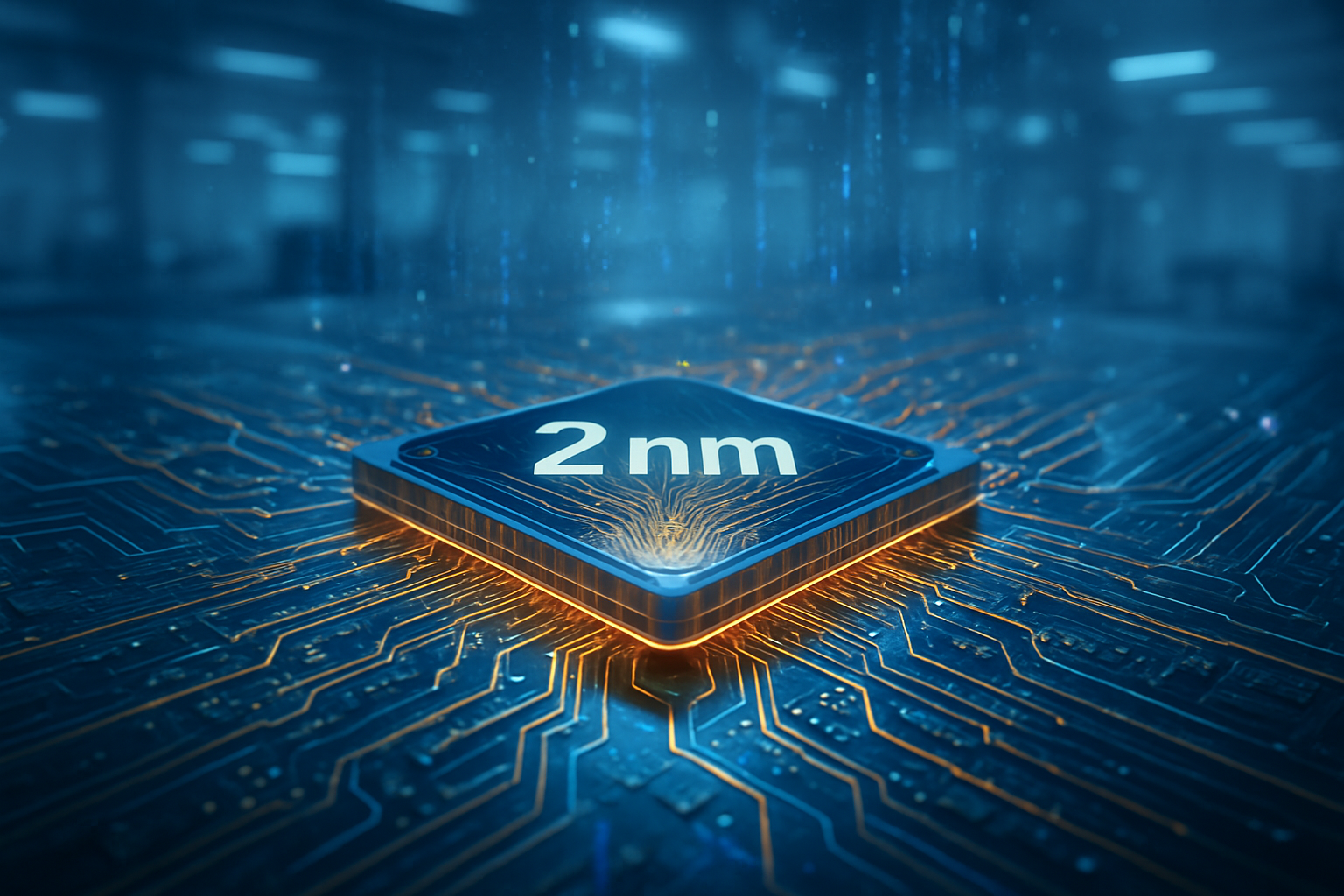
    Technically, the shift is driven by the transition from "Training" to "Reasoning." While 2023 and 2024 were defined by training Large Language Models (LLMs), 2025 saw the rise of "Reasoning AI"—models that perform complex multi-step thinking during inference. These models require massive amounts of memory bandwidth and inter-chip communication, areas where NVIDIA’s proprietary NVLink interconnect technology provides a significant moat. While AMD (NASDAQ: AMD) has made strides with its MI325X and MI350 series, and Intel has attempted to gain ground with its Gaudi 3 accelerators, NVIDIA’s ability to provide a full-stack solution—including the CUDA software layer and Spectrum-X networking—has made it the default choice for hyperscalers.

    Initial reactions from the research community suggest that the industry is no longer just buying "chips," but "time-to-market." The integration of hardware and software allows AI labs to deploy clusters of 100,000+ GPUs and begin training or serving models almost immediately. This "plug-and-play" capability at a massive scale has effectively locked in the world’s largest spenders, including Microsoft (NASDAQ: MSFT), Meta (NASDAQ: META), and Alphabet (NASDAQ: GOOGL), who are currently locked in a "Prisoner's Dilemma" where they must continue to spend record amounts on NVIDIA hardware to avoid falling behind in the AI arms race.

    Competitive Implications and the Shrinking CPU Pie

    The strategic implications for the rest of the semiconductor industry are profound. For Intel (NASDAQ: INTC), the rise of NVIDIA has forced a painful pivot toward its Foundry business. While Intel’s "Panther Lake" CPUs remain competitive in the dwindling market for general-purpose server chips, the company’s Data Center and AI (DCAI) segment has stagnated, hovering around $4 billion per quarter. Intel is now betting its future on becoming the primary manufacturer for other chip designers, including potentially its own rivals, as it struggles to regain its footing in the high-margin AI accelerator market.

    AMD (NASDAQ: AMD) has fared better in terms of market share, successfully capturing nearly 30% of the server CPU market from Intel by late 2025. However, this victory is increasingly viewed as a "king of the hill" battle on a shrinking mountain. As data center budgets shift toward GPUs, the total addressable market for CPUs is not growing at the same rate as the overall AI infrastructure spend. AMD’s Instinct GPU line has seen healthy growth, reaching several billion in revenue, but it still lacks the software ecosystem and networking integration that allows NVIDIA to command 75%+ gross margins.

    Startups and smaller AI labs are also feeling the squeeze. The high cost of NVIDIA’s top-tier Blackwell systems has created a two-tier AI landscape: "compute-rich" giants who can afford the latest $3 million racks, and "compute-poor" entities that must rely on older Hopper (H100) hardware or cloud rentals. This has led to a surge in demand for AI orchestration platforms that can maximize the efficiency of existing hardware, as companies look for ways to extract more performance from their multi-billion dollar investments.

    The Broader AI Landscape: From Components to Sovereign Clouds

    This shift fits into a broader trend of "Sovereign AI," where nations are now building their own domestic data centers to ensure data privacy and technological independence. In late 2025, countries like Saudi Arabia, the UAE, and Japan emerged as major NVIDIA customers, purchasing entire AI factories to fuel their national AI initiatives. This has diversified NVIDIA’s revenue stream beyond the "Big Four" US hyperscalers, further insulating the company from any potential cooling in Silicon Valley venture capital.

    The wider significance of NVIDIA’s $50 billion quarters cannot be overstated. It represents the most rapid reallocation of capital in industrial history. Comparisons are often made to the build-out of the internet in the late 1990s, but with a key difference: the AI build-out is generating immediate, tangible revenue for the infrastructure provider. While the "dot-com" era saw massive spending on fiber optics that took a decade to utilize, NVIDIA’s Blackwell chips are often sold out 12 months in advance, with demand for "Inference-as-a-Service" growing as fast as the hardware can be manufactured.

    However, this dominance has also raised concerns. Regulators in the US and EU have increased their scrutiny of NVIDIA’s "moat," specifically focusing on whether the bundling of CUDA software with hardware constitutes anti-competitive behavior. Furthermore, the sheer energy requirements of these GPU-dense data centers have led to a secondary crisis in power generation, with NVIDIA now frequently partnering with energy companies to secure the gigawatts of electricity needed to run its latest clusters.

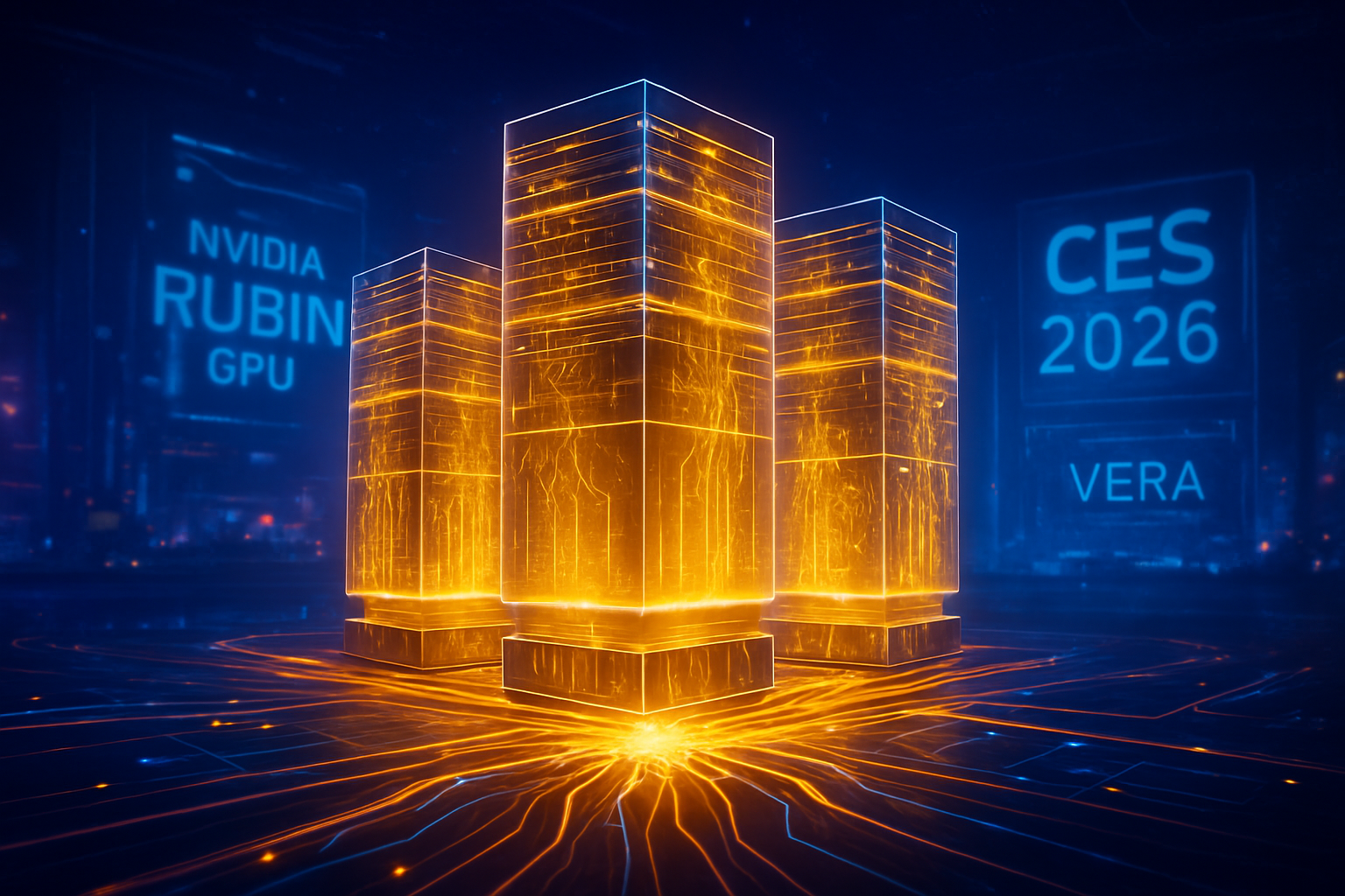
    Future Horizons: Vera Rubin and the $500 Billion Visibility

    Looking ahead to the remainder of 2026 and 2027, NVIDIA has already signaled its next move with the announcement of the "Vera Rubin" platform. Named after the astronomer who discovered evidence of dark matter, the Rubin architecture is expected to focus on "Unified Compute," further blurring the lines between networking, memory, and processing. Experts predict that NVIDIA will continue its transition toward becoming a "Data Center-as-a-Service" company, potentially offering its own cloud capacity to compete directly with the very hyperscalers that are currently its largest customers.

    Near-term developments will likely focus on "Edge AI" and "Physical AI" (robotics). As the cost of inference drops due to Blackwell’s efficiency, we expect to see more complex AI models running locally on devices and within industrial robots. The challenge will be the "power wall"—the physical limit of how much heat can be dissipated and how much electricity can be delivered to a single rack. Addressing this will require breakthroughs in liquid cooling and power delivery, areas where NVIDIA is already investing heavily through its ecosystem of partners.

    A Permanent Shift in the Computing Hierarchy

    The data from early 2026 confirms that NVIDIA is no longer just a chip company; it is the architect of the AI era. By capturing more revenue than the combined forces of the traditional CPU industry, NVIDIA has proved that the future of computing is accelerated, parallel, and deeply integrated. The "CPU-centric" world of the last 40 years has been replaced by an "AI-centric" world where the GPU is the heart of the machine.

    Key takeaways for the coming months include the continued ramp-up of Blackwell, the first real-world benchmarks of the Vera Rubin architecture, and the potential for a "second wave" of AI investment from enterprise customers who are finally moving their AI pilots into full-scale production. While the competition from AMD and the manufacturing pivot of Intel will continue, the "center of gravity" has moved. For the foreseeable future, the world’s digital infrastructure will be built on NVIDIA’s terms.


    This content is intended for informational purposes only and represents analysis of current AI developments.

    TokenRing AI delivers enterprise-grade solutions for multi-agent AI workflow orchestration, AI-powered development tools, and seamless remote collaboration platforms.
    For more information, visit https://www.tokenring.ai/.

  • Intel Reclaims the Silicon Crown: Core Ultra Series 3 ‘Panther Lake’ Debuts at CES 2026 as First US-Made 18A AI PC Chip

    Intel Reclaims the Silicon Crown: Core Ultra Series 3 ‘Panther Lake’ Debuts at CES 2026 as First US-Made 18A AI PC Chip

    In a landmark moment for the global semiconductor industry, Intel (NASDAQ:INTC) officially launched its Core Ultra Series 3 processors, codenamed "Panther Lake," at CES 2026. Unveiled by senior leadership at the Las Vegas tech showcase, Panther Lake represents more than just a seasonal hardware refresh; it is the first consumer-grade silicon built on the Intel 18A process node, manufactured entirely within the United States. This launch marks the culmination of Intel’s ambitious "five nodes in four years" strategy, signaling a definitive return to the forefront of manufacturing technology.

    The immediate significance of Panther Lake lies in its role as the engine for the next generation of "Agentic AI PCs." With a dedicated Neural Processing Unit (NPU) delivering 50 TOPS (Trillions of Operations Per Second) and a total platform throughput of 180 TOPS, Intel is positioning these chips to handle complex, autonomous AI agents locally on the device. By combining cutting-edge domestic manufacturing with unprecedented AI performance, Intel is not only challenging its rivals but also reinforcing the strategic importance of a resilient, US-based semiconductor supply chain.

    The 18A Breakthrough: RibbonFET and PowerVia Take Center Stage

    Technically, Panther Lake is a marvel of modern engineering, representing the first large-scale implementation of two foundational innovations: RibbonFET and PowerVia. RibbonFET is Intel’s implementation of a gate-all-around (GAA) transistor architecture, which replaces the long-standing FinFET design. This allows for better electrostatic control and higher drive current at lower voltages, resulting in a 15% improvement in performance-per-watt over previous generations. Complementing this is PowerVia, the industry's first backside power delivery system. By moving power routing to the back of the wafer, Intel has eliminated traditional bottlenecks in transistor density and reduced voltage droop, allowing the chip to run more efficiently under heavy AI workloads.

    At the heart of Panther Lake’s AI capabilities is the NPU 5 architecture. While the previous generation "Lunar Lake" met the 40 TOPS threshold for Microsoft (NASDAQ:MSFT) Copilot+ certification, Panther Lake pushes the dedicated NPU to 50 TOPS. When the NPU works in tandem with the new Xe3 "Celestial" graphics architecture and the high-performance Cougar Cove CPU cores, the total platform performance reaches a staggering 180 TOPS. This leap is specifically designed to enable "Small Language Models" (SLMs) and vision-action models to run with near-zero latency, allowing for real-time privacy-focused AI assistants that don't rely on the cloud.

    The integrated graphics also see a massive overhaul. The Xe3 Celestial architecture, marketed under the Arc B-Series umbrella, features up to 12 Xe3 cores. Intel claims this provides a 77% increase in gaming performance compared to the Core Ultra 9 285H. Beyond gaming, these GPU cores are equipped with XMX engines that provide the bulk of the platform’s 180 TOPS, making the chip a powerhouse for local generative AI tasks like image creation and video upscaling.

    Initial reactions from the industry have been overwhelmingly positive. Analysts from the AI research community have noted that Panther Lake’s focus on "total platform TOPS" rather than just NPU throughput reflects a more mature understanding of how AI software actually utilizes hardware. By spreading the load across the CPU, GPU, and NPU, Intel is providing developers with a more flexible playground for building the next generation of software.

    Reshaping the Competitive Landscape: Intel vs. The World

    The launch of Panther Lake creates immediate pressure on Intel’s primary competitors: AMD (NASDAQ:AMD), Qualcomm (NASDAQ:QCOM), and Apple (NASDAQ:AAPL). While Qualcomm’s Snapdragon X2 Elite currently holds the lead in raw NPU throughput with 80 TOPS, Intel’s "total platform" approach and superior integrated graphics offer a more balanced package for power users and gamers. AMD’s Ryzen AI 400 series, also debuting at CES 2026, competes closely with a 60 TOPS NPU, but Intel’s transition to the 18A node gives it a density and power efficiency advantage that AMD, still largely reliant on TSMC (NYSE:TSM) for manufacturing, may struggle to match in the short term.

    For tech giants like Dell (NYSE:DELL), HP (NYSE:HPQ), and ASUS, Panther Lake provides the high-performance silicon needed to justify a new upgrade cycle for enterprise and consumer laptops. These manufacturers have already announced over 200 designs based on the new architecture, many of which focus on "AI-first" features like automated workflow orchestration and real-time multi-modal translation. The ability to run these tasks locally reduces cloud costs for enterprises, making Intel-powered AI PCs an attractive proposition for IT departments.

    Furthermore, the success of the 18A node is a massive win for the Intel Foundry business. With Panther Lake proving that 18A is ready for high-volume production, external customers like Amazon (NASDAQ:AMZN) and the U.S. Department of Defense are likely to accelerate their own 18A-based projects. This positions Intel not just as a chip designer, but as a critical manufacturing partner for the entire tech industry, potentially disrupting the long-standing dominance of TSMC in the leading-edge foundry market.

    A Geopolitical Milestone: The Return of US Silicon Leadership

    Beyond the spec sheets, Panther Lake carries immense weight in the broader context of global technology and geopolitics. For the first time in over a decade, the world’s most advanced semiconductor process node is being manufactured in the United States, specifically at Intel’s Fab 52 in Arizona. This is a direct victory for the CHIPS and Science Act, which sought to revitalize domestic manufacturing and reduce reliance on overseas supply chains.

    The strategic importance of this cannot be overstated. As AI becomes a central pillar of national security and economic competitiveness, having a domestic source of leading-edge AI silicon is a critical advantage. The U.S. government’s involvement through the RAMP-C project ensures that the same 18A technology powering consumer laptops will also underpin the next generation of secure defense systems.

    However, this shift also brings concerns regarding the sustainability of such massive energy requirements. The production of 18A chips involves High-NA EUV lithography, a process that is incredibly energy-intensive. As Intel scales this production, the industry will be watching closely to see how the company balances its manufacturing ambitions with its environmental and social governance (ESG) goals. Nevertheless, compared to previous milestones like the introduction of the first 64-bit processors or the shift to multi-core architectures, the move to 18A and integrated AI represents a more fundamental shift in how computing power is generated and deployed.

    The Horizon: From AI PCs to Autonomous Systems

    Looking ahead, Panther Lake is just the beginning of Intel’s 18A journey. The company has already teased its next-generation "Clearwater Forest" Xeon processors for data centers and the future "14A" node, which is expected to push boundaries even further by 2027. In the near term, we can expect to see a surge in "Agentic" software—applications that don't just respond to prompts but proactively manage tasks for the user. With 50+ TOPS of NPU power, these agents will be able to "see" what is on a user's screen and "act" across different applications securely and privately.

    The challenges remaining are largely on the software side. While the hardware is now capable of 180 TOPS, the ecosystem of developers must catch up to utilize this power effectively. We expect to see Microsoft release a major Windows "AI Edition" update later this year that specifically targets the capabilities of Panther Lake and its contemporaries, potentially moving the operating system's core functions into the AI domain.

    Closing the Chapter on the "Foundry Gap"

    In summary, the launch of the Core Ultra Series 3 "Panther Lake" at CES 2026 is a defining moment for Intel and the American tech industry. By successfully delivering a 1.8nm-class processor with a 50 TOPS NPU and high-end integrated graphics, Intel has proved that it can still innovate at the bleeding edge of physics. The 18A node is no longer a roadmap promise; it is a shipping reality that re-establishes Intel as a formidable leader in both chip design and manufacturing.

    As we move into the first quarter of 2026, the industry will be watching the retail performance of these chips and the stability of the 18A yields. If Intel can maintain this momentum, the "Foundry Gap" that has defined the last five years of the semiconductor industry may finally be closed. For now, the AI PC has officially entered its most powerful era yet, and for the first time in a long time, the heart of that innovation is beating in the American Southwest.


    This content is intended for informational purposes only and represents analysis of current AI developments.

    TokenRing AI delivers enterprise-grade solutions for multi-agent AI workflow orchestration, AI-powered development tools, and seamless remote collaboration platforms.
    For more information, visit https://www.tokenring.ai/.

  • The Silicon Super-Cycle: US Implements ‘Managed Bifurcation’ as Semiconductor Market nears $1 Trillion

    The Silicon Super-Cycle: US Implements ‘Managed Bifurcation’ as Semiconductor Market nears $1 Trillion

    As of January 8, 2026, the global semiconductor industry has entered a transformative era defined by what economists call the "Silicon Super-Cycle." With total annual revenue rapidly approaching the $1 trillion milestone, the geopolitical landscape has shifted from a chaotic trade war to a sophisticated state of "managed bifurcation." The United States government, moving beyond passive regulation, has emerged as an active market participant, implementing a groundbreaking revenue-sharing model for AI exports while simultaneously executing strategic interventions to protect domestic interests.

    This new paradigm was punctuated last week by the blocking of a sensitive acquisition and the revelation of a massive federal stake in the nation’s leading chipmaker. These moves signal a definitive end to the era of globalized, borderless silicon and the beginning of a world where advanced compute capacity is treated with the same strategic gravity as nuclear enrichment or oil reserves.

    The Revenue-Sharing Pivot and the 2nm Frontier

    The technical and policy centerpiece of early 2026 is the US Department of Commerce’s "reversal-for-revenue" strategy. In a surprising late-2025 policy shift, the US administration granted NVIDIA Corporation (NASDAQ: NVDA) permission to resume shipments of its high-performance H200 AI chips to select customers in China. However, this comes with a historic caveat: a mandatory 25% "geopolitical risk tax" on every unit sold, paid directly to the US Treasury. This model attempts to balance the commercial needs of American tech giants with the national security goal of funding domestic infrastructure through the profits of competitors.

    Technologically, the industry has reached the 2-nanometer (2nm) milestone. Taiwan Semiconductor Manufacturing Company (NYSE: TSM) reported this week that its N2 process has achieved commercial yields of nearly 70%, significantly ahead of internal projections. This leap allows for a 15% increase in speed or a 30% reduction in power consumption compared to the previous 3nm generation. This advancement is critical as the "Intelligence Economy" demands more efficient hardware to sustain the massive energy requirements of generative AI models that have now moved from text and image generation into real-time, high-fidelity world simulation.

    Initial reactions from the AI research community have been mixed. While the availability of H200-class hardware in China provides a temporary relief valve for global supply chains, industry experts note that the 25% tax effectively creates a "compute divide." Researchers in the West are already eyeing the next generation of Blackwell-Ultra and Rubin architectures, while Chinese firms are being forced to choose between heavily taxed US silicon or domestic alternatives like Huawei’s Ascend series, which Beijing is now mandating for state-level projects.

    Corporate Giants and the Rise of 'Sovereign AI'

    The corporate impact of these shifts is most visible in the partial "nationalization" of Intel Corporation (NASDAQ: INTC). Following a period of financial volatility in late 2025, the US government intervened with an $8.9 billion stock purchase, funded by the Secure Enclave program. This move ensures that the Department of Defense has a guaranteed, domestic source for leading-edge military and intelligence chips. Intel is now effectively a public-private partnership, focused on its Arizona and Oregon "Secure Enclaves" to maintain a "frontier compute" lead over global rivals.

    NVIDIA, meanwhile, is navigating a complex dual-market strategy. While facing a soft boycott in China—where Beijing has directed local firms to halt H200 orders in favor of domestic chips—the company has found a massive new growth engine in the Middle East. In late December 2025, the US greenlit a $1 billion shipment of 35,000 advanced chips to Saudi Arabia’s HUMAIN project and the UAE’s G42. This deal was contingent on the total removal of Chinese hardware from those nations' data centers, illustrating how the US is using its "silicon hegemony" to forge new diplomatic and technological alliances.

    Other major players like Advanced Micro Devices, Inc. (NASDAQ: AMD) and ASML Holding N.V. (NASDAQ: ASML) are adjusting to this highly regulated environment. AMD has seen increased demand for its MI350 series in markets where NVIDIA’s tax-heavy H200s are less competitive, while ASML continues to face tightening restrictions on the export of its High-NA EUV lithography machines, further cementing the "technological moat" around the US and its immediate allies.

    Geopolitical Friction and the 'Third Path'

    The wider significance of these developments lies in the aggressive stance the US is taking against even minor "on-ramps" for foreign influence. On January 2, 2026, a Presidential Executive Order blocked the $3 million acquisition of assets from Emcore Corporation (NASDAQ: EMKR) by HieFo Corp, a firm identified as having ties to Chinese nationals. While the deal was small in dollar terms, the focus was on Emcore’s expertise in indium phosphide (InP) chips—a technology vital for military lasers and advanced sensors. This underscores a policy of "zero-leakage" for dual-use technologies.

    In Europe, a "Third Path" is emerging. All 27 EU member states recently signed a declaration calling for "EU Chips Act 2.0," with a formal review scheduled for the first quarter of 2026. The goal is to secure €20 billion in additional funding to help Europe reach a 20% global market share by 2030. The EU is positioning itself as the global leader in specialized "specialty" chips for the automotive and industrial sectors, attempting to remain a neutral ground while the US and China continue their high-stakes compute race.

    This landscape is a stark departure from the early 2020s. We are no longer seeing a "chip shortage" driven by supply chain hiccups, but a "compute containment" strategy. The US is leveraging its 8:1 advantage in frontier compute capacity to dictate the terms of the global AI rollout, while China counters by leveraging its dominance in the critical mineral supply chains—gallium, germanium, and rare earths—necessary to build the next generation of hardware.

    The Road to 2030: Challenges and Predictions

    Looking ahead, the next 12 to 24 months will likely see the formalization of "CHIPS 2.0" in the United States. Rather than just building factories, the focus is shifting toward fraud risk management and the oversight of the original $50 billion fund. Experts predict that by 2027, the US will attempt to create a "Silicon NATO"—a formal alliance of nations that share compute resources and research while maintaining a unified export front against non-aligned states.

    A major challenge remains the "Malaysia Shift." Companies like Nexperia, currently under pressure due to Chinese ownership, are rapidly moving production to Southeast Asia to avoid "penetrating sanctions." This migration is creating a new semiconductor hub in Malaysia and Vietnam, which could eventually challenge the established order if they can move up the value chain from assembly and testing to actual wafer fabrication.

    Predicting the next move, analysts suggest that the "Intelligence Economy" will drive the semiconductor market toward $1.5 trillion by 2030. The primary hurdle will not be the physics of the chips themselves, but the geopolitical friction of their distribution. As AI models become more integrated into national infrastructure, the "sovereignty" of the silicon they run on will become the most important metric for any nation's security.

    Summary of the New Silicon Order

    The events of early 2026 mark a definitive turning point in the history of technology. The transition from free-market competition to "managed bifurcation" reflects the reality that semiconductors are now the foundational resource of the 21st century. The US government’s active role—from taking stakes in Intel to taxing NVIDIA’s exports—shows that the "invisible hand" of the market has been replaced by the strategic hand of the state.

    Key takeaways for the coming weeks include the EU’s formal decision on Chips Act 2.0 funding and the potential for a Chinese counter-response regarding critical mineral exports. As we monitor these developments, the central question remains: can the world sustain a $1 trillion industry that is increasingly divided by digital iron curtains, or will the cost of bifurcation eventually stifle the very AI revolution it seeks to control?


    This content is intended for informational purposes only and represents analysis of current AI developments.

    TokenRing AI delivers enterprise-grade solutions for multi-agent AI workflow orchestration, AI-powered development tools, and seamless remote collaboration platforms.
    For more information, visit https://www.tokenring.ai/.

  • The Backside Revolution: How PowerVia and A16 Are Rewiring the Future of AI Silicon

    The Backside Revolution: How PowerVia and A16 Are Rewiring the Future of AI Silicon

    As of January 8, 2026, the semiconductor industry has reached a historic inflection point that promises to redefine the limits of artificial intelligence hardware. For decades, chip designers have struggled with a fundamental physical bottleneck: the "front-side" delivery of power, where power lines and signal wires compete for the same cramped real estate on top of transistors. Today, that bottleneck is being shattered as Backside Power Delivery (BSPD) officially enters high-volume manufacturing, led by Intel Corporation (NASDAQ: INTC) and its groundbreaking 18A process.

    The shift to backside power—marketing-branded as "PowerVia" by Intel and "Super PowerRail" by Taiwan Semiconductor Manufacturing Company (NYSE: TSM)—is more than a mere manufacturing tweak; it is a fundamental architectural reorganization of the microchip. By moving the power delivery network to the underside of the silicon wafer, manufacturers are unlocking unprecedented levels of power efficiency and transistor density. This development arrives at a critical moment for the AI industry, where the ravenous energy demands of next-generation Large Language Models (LLMs) have threatened to outpace traditional hardware improvements.

    The Technical Leap: Decoupling Power from Logic

    Intel's 18A process, which reached high-volume manufacturing at Fab 52 in Chandler, Arizona, earlier this month, represents the first commercial deployment of Backside Power Delivery at scale. The core innovation, PowerVia, works by separating the intricate web of signal wires from the power delivery lines. In traditional chips, power must "tunnel" through up to 15 layers of metal interconnects to reach the transistors, leading to significant "voltage droop" and electrical interference. PowerVia eliminates this by routing power through the back of the wafer using Nano-Through Silicon Vias (nTSVs), providing a direct, low-resistance path to the transistors.

    The technical specifications of Intel 18A are formidable. By implementing PowerVia alongside RibbonFET (Gate-All-Around) transistors, Intel has achieved a 30% reduction in voltage droop and a 6% boost in clock frequency at identical power levels compared to previous generations. More importantly for AI chip designers, the technology allows for 90% standard cell utilization, drastically reducing the "wiring congestion" that often forces engineers to leave valuable silicon area empty. This leap in logic density—exceeding 30% over the Intel 3 node—means more AI processing cores can be packed into the same physical footprint.

    Initial reactions from the semiconductor research community have been overwhelmingly positive. Dr. Arati Prabhakar, Director of the White House Office of Science and Technology Policy, noted during a recent briefing that "the successful ramp of 18A is a validation of the 'five nodes in four years' strategy and a pivotal moment for domestic advanced manufacturing." Industry experts at SemiAnalysis have highlighted that Intel’s decision to decouple PowerVia from its first Gate-All-Around node (Intel 20A) allowed the company to de-risk the technology, giving them a roughly 18-month lead over TSMC in mastering the complexities of backside thinning and via alignment.

    The Competitive Landscape: Intel’s First-Mover Advantage vs. TSMC’s A16 Response

    The arrival of 18A has sent shockwaves through the foundry market, placing Intel Corporation (NASDAQ: INTC) in a rare position of technical leadership over TSMC. Intel has already secured major 18A commitments from Microsoft (NASDAQ: MSFT) and Amazon (NASDAQ: AMZN) for their custom AI accelerators, Maieutics and Trainium 3, respectively. By being the first to offer a mature BSPD solution, Intel Foundry is positioning itself as the premier destination for "AI-first" silicon, where thermal management and power delivery are the primary design constraints.

    However, TSMC is not standing still. The world’s largest foundry is preparing its response in the form of the A16 node, scheduled for high-volume manufacturing in the second half of 2026. TSMC’s implementation, known as Super PowerRail, is technically more ambitious than Intel’s PowerVia. While Intel uses nTSVs to connect to the metal layers, TSMC’s Super PowerRail connects the power network directly to the source and drain of the transistors. This "direct-contact" approach is significantly harder to manufacture but is expected to offer an 8-10% speed increase and a 15-20% power reduction, potentially leapfrogging Intel’s performance metrics by late 2026.

    The strategic battle lines are clearly drawn. Nvidia (NASDAQ: NVDA), the undisputed leader in AI hardware, has reportedly signed on as the anchor customer for TSMC’s A16 node to power its 2027 "Feynman" GPU architecture. Meanwhile, Apple (NASDAQ: AAPL) is rumored to be taking a more cautious approach, potentially skipping A16 for its mobile chips to focus on the N2P node, suggesting that backside power is currently viewed as a premium feature specifically optimized for high-performance computing and AI data centers rather than consumer mobile devices.

    Wider Significance: Solving the AI Power Crisis

    The transition to backside power delivery is a critical milestone in the broader AI landscape. As AI models grow in complexity, the "power wall"—the limit at which a chip can no longer be cooled or supplied with enough electricity—has become the primary obstacle to progress. BSPD effectively raises this wall. By reducing IR drop (voltage loss) and improving thermal dissipation, backside power allows AI accelerators to run at higher sustained workloads without throttling. This is essential for training the next generation of "Agentic AI" systems that require constant, high-intensity compute cycles.

    Furthermore, this development marks the end of the "FinFET era" and the beginning of the "Angstrom era." The move to 18A and A16 represents a transition where traditional scaling (making things smaller) is being replaced by architectural scaling (rearranging how things are built). This shift mirrors previous milestones like the introduction of High-K Metal Gate (HKMG) or EUV lithography, both of which were necessary to keep Moore’s Law alive. In 2026, the "Backside Revolution" is the new prerequisite for remaining competitive in the global AI arms race.

    There are, however, concerns regarding the complexity and cost of these new processes. Backside power requires extremely precise wafer thinning—grinding the silicon down to a fraction of its original thickness—and complex bonding techniques. These steps increase the risk of wafer breakage and lower initial yields. While Intel has reported healthy 18A yields in the 55-65% range, the high cost of these chips may further consolidate power in the hands of "Big Tech" giants like Alphabet (NASDAQ: GOOGL) and Meta (NASDAQ: META), who are the only ones capable of affording the multi-billion dollar design and fabrication costs associated with 1.6nm and 1.8nm silicon.

    The Road Ahead: 1.4nm and the Future of AI Accelerators

    Looking toward the late 2020s, the trajectory of backside power is clear: it will become the standard for all high-performance logic. Intel is already planning its "14A" node for 2027, which will refine PowerVia with even denser interconnects. Simultaneously, Samsung Electronics (OTC: SSNLF) is preparing its SF2Z node for 2027, which will integrate its own version of BSPDN into its third-generation Gate-All-Around (MBCFET) architecture. Samsung’s entry will likely trigger a price war in the advanced foundry space, potentially making backside power more accessible to mid-sized AI startups and specialized ASIC designers.

    Beyond 2026, we expect to see "Backside Power 2.0," where manufacturers begin to move other components to the back of the wafer, such as decoupling capacitors or even certain types of memory (like RRAM). This could lead to "3D-stacked" AI chips where the logic is sandwiched between a backside power delivery layer and a front-side memory cache, creating a truly three-dimensional computing environment. The primary challenge remains the thermal density; as chips become more efficient at delivering power, they also become more concentrated heat sources, necessitating new liquid cooling or "on-chip" cooling technologies.

    Conclusion: A New Foundation for Artificial Intelligence

    The arrival of Intel’s 18A and the looming shadow of TSMC’s A16 mark the beginning of a new chapter in semiconductor history. Backside Power Delivery has transitioned from a laboratory curiosity to a commercial reality, providing the electrical foundation upon which the next decade of AI innovation will be built. By solving the "routing congestion" and "voltage droop" issues that have plagued chip design for years, PowerVia and Super PowerRail are enabling a new class of processors that are faster, cooler, and more efficient.

    The significance of this development cannot be overstated. In the history of AI, we will look back at 2026 as the year the industry "flipped the chip" to keep the promise of exponential growth alive. For investors and tech enthusiasts, the coming months will be defined by the ramp-up of Intel’s Panther Lake and Clearwater Forest processors, providing the first real-world benchmarks of what backside power can do. As TSMC prepares its A16 risk production in the first half of 2026, the battle for silicon supremacy has never been more intense—or more vital to the future of technology.


    This content is intended for informational purposes only and represents analysis of current AI developments.

    TokenRing AI delivers enterprise-grade solutions for multi-agent AI workflow orchestration, AI-powered development tools, and seamless remote collaboration platforms.
    For more information, visit https://www.tokenring.ai/.

  • The Silicon Divorce: Hyperscalers Launch Custom AI Chips to Break NVIDIA’s Monopoly

    The Silicon Divorce: Hyperscalers Launch Custom AI Chips to Break NVIDIA’s Monopoly

    As the calendar turns to early 2026, the artificial intelligence industry is witnessing its most significant infrastructure shift since the start of the generative AI boom. For years, the "NVIDIA tax"—the high cost and limited supply of high-end GPUs—has been the primary bottleneck for tech giants. Today, that era of total dependence is coming to a close. Google, a subsidiary of Alphabet Inc. (NASDAQ: GOOGL), and Meta Platforms, Inc. (NASDAQ: META), have officially moved their latest generations of custom silicon, the TPU v6 (Trillium) and MTIA v3, into mass production, signaling a major transition toward vertical integration in the cloud.

    This movement represents more than just a search for cost savings; it is a fundamental architectural pivot. By designing chips specifically for their own internal workloads—such as recommendation algorithms, large language model (LLM) inference, and massive-scale training—hyperscalers are achieving performance-per-watt efficiencies that general-purpose GPUs struggle to match. As these custom accelerators flood data centers throughout 2026, the competitive landscape for AI infrastructure is being rewritten, challenging the long-standing dominance of NVIDIA (NASDAQ: NVDA) in the enterprise cloud.

    Technical Prowess: The Rise of Specialized ASICs

    The Google TPU v6, codenamed Trillium, has entered 2026 as the volume leader in Google’s fleet, with production scaling to over 1.6 million units this year. Trillium represents a massive leap forward, boasting a 4.7x increase in peak compute performance per chip compared to its predecessor, the TPU v5e. Technically, the TPU v6 is optimized for the "SparseCore" architecture, which is critical for the massive embedding tables used in modern recommendation systems and the "Mixture of Experts" (MoE) models that power the latest iterations of Gemini. By doubling the High Bandwidth Memory (HBM) capacity and bandwidth, Google has created a chip that excels at the high-throughput demands of 2026’s multimodal AI agents.

    Simultaneously, Meta’s MTIA v3 (Meta Training and Inference Accelerator) has moved from testing into full-scale deployment. Unlike earlier versions which were primarily focused on inference, the MTIA v3 is a full-stack training and inference solution. Built on a refined 3nm process, the MTIA v3 utilizes a custom RISC-V-based matrix compute grid. This architecture is specifically tuned to run Meta’s PyTorch-based workloads with surgical precision. Early benchmarks suggest that the MTIA v3 provides a 3x performance boost over its predecessor, allowing Meta to train its Llama-series models with significantly lower latency and power consumption than standard GPU clusters.

    This shift differs from previous approaches because it moves away from the "one-size-fits-all" philosophy of the GPU. While NVIDIA’s Blackwell architecture remains the gold standard for raw, versatile power, the TPU v6 and MTIA v3 are Application-Specific Integrated Circuits (ASICs). They strip away the hardware overhead required for general-purpose graphics or scientific simulation, focusing entirely on the tensor operations and memory management required for neural networks. Industry experts have noted that while a GPU is a "Swiss Army knife," these new chips are high-precision scalpels, designed to perform specific AI tasks with nearly double the cost-efficiency of general hardware.

    The reaction from the AI research community has been one of cautious optimism. Researchers at major labs have highlighted that the proliferation of custom silicon is finally easing the "compute crunch" that defined 2024 and 2025. However, the transition has required a significant software evolution. The success of these chips in 2026 is largely attributed to the maturity of open-source compilers like OpenAI’s Triton and the release of PyTorch 3.0, which have effectively neutralized NVIDIA's "CUDA moat" by making it easier for developers to port code across different hardware architectures without massive performance penalties.

    Market Repercussions: Challenging the NVIDIA Hegemony

    The strategic implications for the tech giants are profound. For companies like Google and Meta, producing their own silicon is a defensive necessity. By 2026, inference workloads—the process of running a trained model for users—are projected to account for nearly 70% of all AI-related compute. Because custom ASICs like the TPU v6 are roughly 1.4x to 2x more cost-efficient than GPUs for inference, Google can offer its AI services at a lower price point than competitors who are still paying a premium for third-party hardware. This vertical integration provides a massive margin advantage in the increasingly commoditized market for LLM API calls.

    NVIDIA is already feeling the pressure. While the company still maintains a commanding lead in the highest-end frontier model training, its market share in the broader AI accelerator space is expected to slip from its peak of 95% down toward 75-80% by the end of 2026. The rise of "Hyperscaler Silicon" means that Amazon.com, Inc. (NASDAQ: AMZN) and Microsoft Corporation (NASDAQ: MSFT) are also less reliant on NVIDIA’s roadmap. Amazon’s Trainium 3 (Trn3) has also reached mass deployment this year, achieving performance parity with NVIDIA’s Blackwell racks for specific training tasks, further crowding the high-end market.

    For startups and smaller AI labs, this development is a double-edged sword. On one hand, the increased competition is driving down the cost of cloud compute, making it cheaper to build and deploy new models. On the other hand, the best-performing hardware is increasingly "walled off" within specific cloud ecosystems. A startup using Google Cloud may find that their models run significantly faster on TPU v6, but moving those same models to Microsoft Azure’s Maia 200 silicon could require significant re-optimization. This creates a new kind of "vendor lock-in" based on hardware architecture rather than just software APIs.

    Strategic positioning in 2026 is now defined by "silicon sovereignty." Meta, for instance, has stated its goal to migrate 100% of its internal recommendation traffic to MTIA by 2027. By owning the hardware, Meta can optimize its social media algorithms at a level of granularity that was previously impossible. This allows for more complex, real-time personalization of content without a corresponding explosion in data center energy costs, giving Meta a distinct advantage in the battle for user attention and advertising efficiency.

    The Industrialization of AI

    The shift toward custom silicon in 2026 marks the "industrialization phase" of the AI revolution. In the early days, the industry relied on whatever hardware was available—primarily gaming GPUs. Today, the infrastructure is being purpose-built for the task at hand. This mirrors historical trends in other industries, such as the transition from general-purpose steam engines to specialized internal combustion engines designed for specific types of vehicles. It signifies that AI has moved from a research curiosity to the foundational utility of the modern economy.

    Environmental concerns are also a major driver of this trend. As global energy grids struggle to keep up with the demands of massive data centers, the efficiency gains of chips like the TPU v6 are critical. Custom silicon allows hyperscalers to do more with less power, which is essential for meeting the sustainability targets that many of these corporations have set for the end of the decade. The ability to perform 4.7x more compute per watt isn't just a financial metric; it's a regulatory and social necessity in a world increasingly conscious of the carbon footprint of digital services.

    However, this transition also raises concerns about the concentration of power. As the "Big Five" tech companies develop their own proprietary hardware, the barrier to entry for a new cloud provider becomes nearly insurmountable. It is no longer enough to buy a fleet of GPUs; a competitor would now need to invest billions in R&D to design their own chips just to achieve price parity. This could lead to a permanent oligopoly in the AI infrastructure space, where only a handful of companies possess the specialized hardware required to run the world's most advanced intelligence systems.

    Comparatively, this milestone is being viewed as the "Post-GPU Era." While GPUs will likely always have a place in the market due to their versatility and the massive ecosystem surrounding them, they are no longer the undisputed kings of the data center. The successful mass production of TPU v6 and MTIA v3 in 2026 serves as a clear signal that the future of AI is heterogeneous. We are moving toward a world where the hardware is as specialized as the software it runs, leading to a more efficient, albeit more fragmented, technological landscape.

    The Road to 2027 and Beyond

    Looking ahead, the silicon wars are only expected to intensify. Even as TPU v6 and MTIA v3 dominate the headlines today, Google is already beginning the limited rollout of TPU v7 (Ironwood), its first 3nm chip designed for massive rack-scale computing. Experts predict that by 2027, we will see the first 2nm AI chips entering the prototyping phase, pushing the limits of Moore’s Law even further. The focus will likely shift from raw compute power to "interconnect density"—how fast these thousands of custom chips can talk to one another to form a single, giant "planetary computer."

    We also expect to see these custom designs move closer to the "edge." While 2026 is the year of the data center chip, the architectural lessons learned from MTIA and TPU are already being applied to mobile processors and local AI accelerators. This will eventually lead to a seamless continuum of AI hardware, where a model can be trained on a TPU v6 cluster and then deployed on a specialized mobile NPU (Neural Processing Unit) that shares the same underlying architecture, ensuring maximum efficiency from the cloud to the pocket.

    The primary challenge moving forward will be the talent war. Designing world-class silicon requires a highly specialized workforce of chip architects and physical design engineers. As hyperscalers continue to expand their hardware divisions, the competition for this talent will be fierce. Furthermore, the geopolitical stability of the semiconductor supply chain remains a lingering concern. While Google and Meta design their chips in-house, they still rely on foundries like TSMC for production. Any disruption in the global supply chain could stall the ambitious rollout plans for 2027 and beyond.

    Conclusion: A New Era of Infrastructure

    The mass production of Google’s TPU v6 and Meta’s MTIA v3 in early 2026 represents a pivotal moment in the history of computing. It marks the end of NVIDIA’s absolute monopoly and the beginning of a new era of vertical integration and specialized hardware. By taking control of their own silicon, hyperscalers are not only reducing costs but are also unlocking new levels of performance that will define the next generation of AI applications.

    In terms of significance, 2026 will be remembered as the year the "AI infrastructure stack" was finally decoupled from the gaming GPU heritage. The move to ASICs represents a maturation of the field, where efficiency and specialization are the new metrics of success. This development ensures that the rapid pace of AI advancement can continue even as the physical and economic limits of general-purpose hardware are reached.

    In the coming months, the industry will be watching closely to see how NVIDIA responds with its upcoming Vera Rubin (R100) architecture and how quickly other players like Microsoft and AWS can scale their own designs. The battle for the heart of the AI data center is no longer just about who has the most chips, but who has the smartest ones. The silicon divorce is finalized, and the future of intelligence is now being forged in custom-designed silicon.


    This content is intended for informational purposes only and represents analysis of current AI developments.

    TokenRing AI delivers enterprise-grade solutions for multi-agent AI workflow orchestration, AI-powered development tools, and seamless remote collaboration platforms.
    For more information, visit https://www.tokenring.ai/.

  • American Silicon: Micron’s Groundbreaking New York Megafab Secures the Future of AI Memory

    American Silicon: Micron’s Groundbreaking New York Megafab Secures the Future of AI Memory

    The global race for artificial intelligence supremacy has officially shifted its center of gravity to the American heartland. As of January 8, 2026, the domestic semiconductor landscape has reached a historic milestone with Micron Technology, Inc. (NASDAQ: MU) preparing to break ground on its massive New York "megafab" in Clay, New York. This project, alongside the rapidly advancing construction of its leading-edge facility in Boise, Idaho, represents a seismic shift in the production of High Bandwidth Memory (HBM)—the specialized silicon essential for powering the world’s most advanced AI data centers.

    This "Made in USA" memory push is more than just a construction project; it is a strategic realignment of the global supply chain. For years, the HBM market was dominated by South Korean giants, leaving American AI leaders vulnerable to geopolitical shifts and logistical bottlenecks. Backed by billions in federal support from the CHIPS and Science Act, Micron’s expansion is designed to ensure that the "brains" of the AI revolution are not only designed in the U.S. but manufactured and packaged on American soil, providing a stable foundation for the next decade of computing.

    Scaling the Heights: From HBM3E to the HBM4 Revolution

    The technical specifications of these new facilities are staggering. The New York site, which will see its official groundbreaking on January 16, 2026, is a $100 billion multi-decade investment designed to eventually house four massive fabrication plants. Meanwhile, the Boise, Idaho, fab—which broke ground in late 2022—is already nearing completion of its exterior structure. By fiscal year 2027, the Boise site is expected to begin volume production of DRAM using Micron’s proprietary 1-beta and upcoming 1-gamma nodes. These facilities are specifically optimized for HBM, which stacks multiple layers of DRAM vertically to achieve the massive data throughput required by modern GPUs.

    As the industry transitions from HBM3E to the next-generation HBM4 standard in early 2026, Micron has positioned itself as a leader in power efficiency. While competitors like SK Hynix Inc. (KRX: 000660) and Samsung Electronics Co., Ltd. (KRX: 005930) have historically held larger market shares, Micron’s 12-high (12-Hi) HBM3E stacks have gained significant traction by offering 30% lower power consumption than the industry average. This efficiency is critical for data center operators who are increasingly constrained by thermal limits and energy costs. The upcoming HBM4 transition will double the interface width to 2048-bit, pushing bandwidth beyond 2.0 TB/s, a requirement for the next generation of AI architectures.

    Reshaping the Competitive Landscape for AI Giants

    The implications for the broader tech industry are profound. For AI heavyweights like NVIDIA Corporation (NASDAQ: NVDA) and Advanced Micro Devices, Inc. (NASDAQ: AMD), a domestic source of HBM reduces the "single-source" risk associated with relying almost exclusively on overseas suppliers. NVIDIA, which qualified Micron’s HBM3E for its Blackwell Ultra GPUs in late 2024, stands to benefit from a more resilient supply chain that can better withstand regional conflicts or trade disruptions. By having high-volume memory production co-located in the same hemisphere as the primary chip designers, the industry can expect faster iteration cycles and more integrated co-design of memory and logic.

    However, this shift also intensifies the rivalry between the "Big Three" memory makers. SK Hynix currently maintains a dominant 55-60% share of the HBM market, leveraging its Mass Reflow Molded Underfill (MR-MUF) bonding technology. Samsung has also made a massive push, recently announcing mass production of HBM4 using its "1c" process. Micron’s strategic advantage lies in its aggressive adoption of the CHIPS Act incentives to build the most modern, automated fabs in the world. Micron aims to capture 30% of the HBM4 market by the end of 2026, a goal that would significantly erode the current duopoly held by its Korean rivals.

    The CHIPS Act as a Catalyst for AI Sovereignty

    The rapid progress of these facilities would likely have been impossible without the $6.165 billion in direct funding and $7.5 billion in loans finalized under the CHIPS and Science Act in late 2024. This federal intervention represents a pivot toward "AI Sovereignty"—the idea that a nation’s economic and national security depends on its ability to produce the fundamental building blocks of artificial intelligence domestically. By subsidizing the high capital expenditures of these fabs, the U.S. government is effectively de-risking the transition to a more localized manufacturing model.

    Beyond the immediate economic impact, the Micron expansion addresses a critical vulnerability in the AI landscape: advanced packaging. Historically, even if chips were designed in the U.S., they often had to be sent to Asia for the complex stacking and bonding required for HBM. Micron’s new facilities will include advanced packaging capabilities, closing the "missing link" in the domestic ecosystem. This fits into a broader global trend of "techno-nationalism," where regions like the EU and Japan are also racing to subsidize their own semiconductor hubs to prevent being left behind in the AI-driven industrial revolution.

    The Horizon: HBM4 and the Path to 2030

    Looking ahead, the next 18 to 24 months will be defined by the mass production of HBM4. While the New York megafab is a long-term play—with initial production now projected for late 2030 due to the immense scale of the project—the Boise facility will serve as the immediate vanguard for U.S.-made memory. Industry experts predict that by 2027, the synergy between Micron’s R&D headquarters and its new Boise fab will allow for "lab-to-fab" transitions that are months faster than the current industry standard.

    The primary challenges remaining are labor and infrastructure. Building and operating these facilities requires tens of thousands of highly skilled engineers and technicians. Micron has already launched massive workforce development initiatives in New York and Idaho, but the talent gap remains a significant concern for the 2030 timeline. Furthermore, the transition to sub-10nm DRAM nodes will require the successful integration of High-NA EUV lithography, a technical hurdle that will test the limits of Micron’s engineering prowess as it seeks to maintain its power-efficiency lead.

    A New Chapter in Semiconductor History

    Micron’s groundbreaking in New York and the progress in Idaho mark the beginning of a new chapter in American industrial history. By successfully leveraging public-private partnerships, the U.S. is on a path to reclaim its position as a manufacturing powerhouse for the most critical components of the digital age. The goal of producing 40% of the company’s global DRAM in the U.S. by the mid-2030s is an ambitious target that, if achieved, will fundamentally alter the economics of the AI industry.

    In the coming weeks, all eyes will be on the official New York groundbreaking on January 16. This event will serve as a symbolic "go" signal for one of the largest construction projects in human history. As these fabs rise, they will not only produce silicon but also provide the essential infrastructure needed to sustain the current AI boom. For investors, policymakers, and tech leaders, the message is clear: the future of AI memory is being forged in America.


    This content is intended for informational purposes only and represents analysis of current AI developments.

    TokenRing AI delivers enterprise-grade solutions for multi-agent AI workflow orchestration, AI-powered development tools, and seamless remote collaboration platforms.
    For more information, visit https://www.tokenring.ai/.

  • Qualcomm Shatters AI PC Performance Barriers with Snapdragon X2 Elite Launch at CES 2026

    Qualcomm Shatters AI PC Performance Barriers with Snapdragon X2 Elite Launch at CES 2026

    The landscape of personal computing has undergone a seismic shift as Qualcomm (NASDAQ: QCOM) officially unveiled its next-generation Snapdragon X2 Elite and Snapdragon X2 Plus processors at CES 2026. This announcement marks a definitive turning point in the "AI PC" era, with Qualcomm delivering a staggering 80 TOPS (Trillions of Operations Per Second) of dedicated NPU performance—far exceeding the initial industry expectations of 50 TOPS. By standardizing this high-tier AI processing power across both its flagship and mid-range "Plus" silicon, Qualcomm is making a bold play to commoditize advanced on-device AI and dismantle the long-standing x86 hegemony in the Windows ecosystem.

    The immediate significance of the X2 series lies in its ability to power "Agentic AI"—background digital entities capable of executing complex, multi-step workflows autonomously. While previous generations focused on simple image generation or background blur, the Snapdragon X2 is designed to manage entire productivity chains, such as cross-referencing a week of emails to draft a project proposal while simultaneously monitoring local security threats. This launch effectively signals the end of the experimental phase for Windows-on-ARM, positioning Qualcomm not just as a mobile chipmaker entering the PC space, but as the primary architect of the modern AI workstation.

    Architectural Leap: The 80 TOPS Standard

    The technical architecture of the Snapdragon X2 series represents a complete overhaul of the initial Oryon design. Built on TSMC’s cutting-edge 3nm (N3P/N3X) process, the X2 Elite features the 3rd Generation Oryon CPU, which has transitioned to a sophisticated tiered core design. Unlike the first generation’s uniform core structure, the X2 Elite utilizes a "Big-Medium-Little" configuration, featuring high-frequency "Prime" cores that boost up to 5.0 GHz for bursty workloads, alongside dedicated efficiency cores that handle background tasks with minimal power draw. This architectural shift allows for a 43% reduction in power consumption compared to the previous Snapdragon X Elite while delivering a 25% increase in multi-threaded performance.

    At the heart of the silicon is the upgraded Hexagon NPU, which now delivers a uniform 80 TOPS across the entire product stack, including the 10-core and 6-core Snapdragon X2 Plus variants. This is a massive 78% generational leap in AI throughput. Furthermore, Qualcomm has integrated a new "Matrix Engine" directly into the CPU clusters. This engine is designed to handle "micro-AI" tasks—such as real-time language translation or UI predictive modeling—without needing to engage the main NPU, thereby reducing latency and further preserving battery life. Initial benchmarks from the AI research community show the X2 Plus 10-core scoring over 4,100 points in UL Procyon AI tests, nearly doubling the performance of current-gen competitors.

    Industry experts have reacted with particular interest to the X2 Elite's on-package memory integration. High-end "Extreme" SKUs now offer up to 128GB of LPDDR5x memory directly on the chip substrate, providing a massive 228 GB/s of bandwidth. This is a critical technical requirement for running Large Language Models (LLMs) with billions of parameters locally, ensuring that user data never has to leave the device for processing. By solving the memory bottleneck that plagued earlier AI PCs, Qualcomm has created a platform that can run sophisticated, private AI models with the same fluid responsiveness as cloud-based alternatives.

    Disrupting the x86 Hegemony

    Qualcomm’s aggressive push is creating a "silicon bloodbath" for traditional incumbents Intel (NASDAQ: INTC) and AMD (NASDAQ: AMD). For decades, the Windows market was defined by the x86 instruction set, but the X2 series' combination of 80 TOPS and 25-hour battery life is forcing a rapid re-evaluation. Intel’s latest "Panther Lake" chips, while highly capable, currently peak at 50 TOPS for their NPU, leaving a significant performance gap in specialized AI tasks. While Intel and AMD still hold the lead in legacy gaming and high-end workstation niches, Qualcomm is successfully capturing the high-volume "prosumer" and enterprise laptop segments that prioritize mobility and AI-driven productivity.

    The competitive landscape is further complicated by Qualcomm’s strategic focus on the enterprise market through its new "Snapdragon Guardian" technology. This hardware-level management suite directly challenges Intel’s vPro, offering IT departments the ability to remote-wipe, update, and secure laptops via the chip’s integrated 5G modem, even when the device is powered down. This move targets the lucrative corporate fleet market, where Intel has historically been unassailable. By offering better AI performance and superior remote management, Qualcomm is giving CIOs a compelling reason to switch architectures for the first time in twenty years.

    Major PC manufacturers like Dell (NYSE: DELL), HP (NYSE: HPQ), and Lenovo are the primary beneficiaries of this shift, as they can now offer a diverse range of "AI-first" laptops that compete directly with Apple's (NASDAQ: AAPL) MacBook Pro in terms of efficiency and power. Microsoft (NASDAQ: MSFT) also stands to gain immensely; the Snapdragon X2 provides the ideal hardware target for the next evolution of Windows 11 and the rumored "Windows 12," which are expected to lean even more heavily into integrated Copilot features that require the high TOPS count Qualcomm now provides as a standard.

    The End of the "App Gap" and the Rise of Local AI

    The broader significance of the Snapdragon X2 launch is the definitive resolution of the "App Gap" that once hindered ARM-based Windows devices. As of early 2026, Microsoft reports that users spend over 90% of their time in native ARM64 applications. With the Adobe Creative Cloud, Microsoft 365, and even specialized CAD software now running natively, the technical friction of switching from Intel to Qualcomm has virtually vanished. Furthermore, Qualcomm’s "Prism" emulation layer has matured to the point where 90% of the top-played Windows games run with minimal performance loss, effectively removing the last major barrier to consumer adoption.

    This development also marks a shift in how the industry defines "performance." We are moving away from raw CPU clock speeds and toward "AI Utility." The ability of the Snapdragon X2 to run 10-billion parameter models locally has profound implications for data privacy and security. By moving AI processing from the cloud to the edge, Qualcomm is addressing growing public concerns regarding data harvesting by major AI labs. This "Local-First" AI movement could fundamentally change the business models of SaaS companies, shifting the value from cloud subscriptions to high-performance local hardware.

    However, this transition is not without concerns. The rapid obsolescence of non-AI PCs could lead to a massive wave of electronic waste as corporations and consumers rush to upgrade to "NPU-capable" hardware. Additionally, the fragmentation of the Windows ecosystem between x86 and ARM, while narrowing, still presents challenges for niche software developers who must now maintain two separate codebases or rely on emulation. Despite these hurdles, the Snapdragon X2 represents the most significant milestone in PC architecture since the introduction of multi-core processing, signaling a future where the CPU is merely a support structure for the NPU.

    Future Horizons: From Laptops to the Edge

    Looking ahead, the next 12 to 24 months will likely see Qualcomm attempt to push the Snapdragon X2 architecture into even more form factors. Rumors are already circulating about a "Snapdragon X2 Ultra" designed for fanless desktop "mini-PCs" and high-end tablets that could rival the iPad Pro. In the long term, Qualcomm has stated its goal is to capture 50% of the Windows laptop market by 2029. To achieve this, the company will need to continue scaling its production and maintaining its lead in NPU performance as Intel and AMD inevitably close the gap with their 2027 and 2028 roadmaps.

    We can also expect to see the emergence of "Multi-Agent" OS environments. With 80 TOPS available locally, developers are likely to build software that utilizes multiple specialized AI agents working in parallel—one for security, one for creative assistance, and one for data management—all running simultaneously on the Hexagon NPU. The challenge for Qualcomm will be ensuring that the software ecosystem can actually utilize this massive overhead. Currently, the hardware is significantly ahead of the software; the "killer app" for an 80 TOPS NPU is still in development, but the headroom provided by the X2 series ensures that when it arrives, the hardware will be ready.

    Conclusion: A New Era of Silicon

    The launch of the Snapdragon X2 Elite and Plus chips is more than just a seasonal hardware refresh; it is an assertive declaration of Qualcomm's intent to lead the personal computing industry. By delivering 80 TOPS of NPU performance and a 3nm architecture that prioritizes efficiency without sacrificing power, Qualcomm has set a new benchmark that its competitors are now scrambling to meet. The standardization of high-end AI processing across its entire lineup ensures that the "AI PC" is no longer a luxury tier but the new baseline for all Windows users.

    As we move through 2026, the key metrics to watch will be Qualcomm's enterprise adoption rates and the continued evolution of Microsoft’s AI integration. If the Snapdragon X2 can maintain its momentum and continue to secure design wins from major OEMs, the decades-long "Wintel" era may finally be giving way to a more diverse, AI-centric silicon landscape. For now, Qualcomm holds the performance crown, and the rest of the industry is playing catch-up in a race where the finish line is constantly being moved by the rapid advancement of artificial intelligence.


    This content is intended for informational purposes only and represents analysis of current AI developments.

    TokenRing AI delivers enterprise-grade solutions for multi-agent AI workflow orchestration, AI-powered development tools, and seamless remote collaboration platforms. For more information, visit https://www.tokenring.ai/.

  • Shattering the Silicon Ceiling: Tower Semiconductor and LightIC Unveil Photonics Breakthrough to Power the Next Decade of AI and Autonomy

    Shattering the Silicon Ceiling: Tower Semiconductor and LightIC Unveil Photonics Breakthrough to Power the Next Decade of AI and Autonomy

    In a landmark announcement that signals a paradigm shift for both artificial intelligence infrastructure and autonomous mobility, Tower Semiconductor (NASDAQ: TSEM) and LightIC Technologies have unveiled a strategic partnership to mass-produce the world’s first monolithic 4D FMCW LiDAR and high-bandwidth optical interconnect chips. Announced on January 5, 2026, just days ahead of the Consumer Electronics Show (CES), this collaboration leverages Tower’s advanced 300mm silicon photonics (SiPho) foundry platform to integrate entire "optical benches"—lasers, modulators, and detectors—directly onto a single silicon substrate.

    The immediate significance of this development cannot be overstated. By successfully transitioning silicon photonics from experimental lab settings to high-volume manufacturing, the partnership addresses the two most critical bottlenecks in modern technology: the "memory wall" that limits AI model scaling in data centers and the high cost and unreliability of traditional sensing for autonomous vehicles. This breakthrough promises to slash power consumption in AI factories while providing self-driving systems with the "velocity awareness" required for safe urban navigation, effectively bridging the gap between digital and physical AI.

    The Technical Leap: 4D FMCW and the End of the Copper Era

    At the heart of the Tower-LightIC partnership is the commercialization of Frequency-Modulated Continuous-Wave (FMCW) LiDAR, a technology that differs fundamentally from the Time-of-Flight (ToF) systems currently used by most automotive manufacturers. While ToF LiDAR pulses light to measure distance, the new LightIC "Lark" and "FR60" chips utilize a continuous wave of light to measure both distance and instantaneous velocity—the fourth dimension—simultaneously for every pixel. This coherent detection method ensures that the sensors are immune to interference from sunlight or other LiDAR systems, a persistent challenge for existing technologies.

    Technically, the integration is achieved using Tower Semiconductor's PH18 process, which allows for the monolithic integration of III-V lasers with silicon-based optical components. The resulting "Lark" automotive chip boasts a detection range of up to 500 meters with a velocity precision of 0.05 meters per second. This level of precision allows a vehicle's AI to instantly distinguish between a stationary object and a pedestrian stepping into a lane, significantly reducing the "perception latency" that currently plagues autonomous driving stacks.

    Furthermore, the same silicon photonics platform is being applied to solve the data bottleneck within AI data centers. As AI models grow in complexity, the traditional copper interconnects used to move data between GPUs and High Bandwidth Memory (HBM) have become a liability, consuming excessive power and generating heat. The new optical interconnect chips enable multi-wavelength laser sources that provide bandwidth of up to 3.2 Tbps. By moving data via light rather than electricity, these chips reduce interconnect latency to a staggering 5 nanoseconds per meter, compared to the 15-20 picajoules per bit required by standard pluggable optics.

    Initial reactions from the AI research community have been overwhelmingly positive. Dr. Elena Vance, a senior researcher in photonics, noted that "the ability to manufacture these components on standard 300mm wafers at Tower's scale is the 'holy grail' of the industry. We are finally moving away from discrete, bulky optical components toward a truly integrated, solid-state future."

    Market Disruption: A New Hierarchy in AI Infrastructure

    The strategic alliance between Tower Semiconductor and LightIC creates immediate competitive pressure for industry giants like Nvidia (NASDAQ: NVDA), Marvell Technology (NASDAQ: MRVL), and Broadcom (NASDAQ: AVGO). While these companies have dominated the AI hardware space, the shift toward Co-Packaged Optics (CPO) and integrated silicon photonics threatens to disrupt established supply chains. Companies that can integrate photonics directly into their chipsets will hold a significant advantage in power efficiency and compute density.

    For data center operators like Amazon (NASDAQ: AMZN), Google (NASDAQ: GOOGL), and Meta (NASDAQ: META), this breakthrough offers a path toward "Green AI." As energy consumption in AI factories becomes a regulatory and financial hurdle, the transition to optical interconnects allows these giants to scale their clusters without hitting a thermal ceiling. The lower power profile of the Tower-LightIC chips could potentially reduce the total cost of ownership (TCO) for massive AI clusters by as much as 30% over a five-year period.

    In the automotive sector, the availability of low-cost, high-performance 4D LiDAR could democratize Level 4 and Level 5 autonomy. Currently, high-end LiDAR systems can cost thousands of dollars per unit, limiting them to luxury vehicles or experimental fleets. LightIC’s FR60 chip, designed for compact robotics and mass-market vehicles, aims to bring this cost down to a point where it can be standard equipment in entry-level consumer cars. This puts pressure on traditional sensor companies and may force a consolidation in the LiDAR market as solid-state silicon photonics becomes the dominant architecture.

    The Broader Significance: Toward "Physical AI" and Sustainability

    The convergence of sensing and communication on a single silicon platform marks a major milestone in the evolution of "Physical AI"—the application of artificial intelligence to the physical world through robotics and autonomous systems. By providing robots and vehicles with human-like (or better-than-human) perception at a fraction of the current energy cost, this breakthrough accelerates the timeline for truly autonomous logistics and urban mobility.

    This development also fits into the broader trend of "Compute-as-a-Light-Source." For years, the industry has warned of the "End of Moore’s Law" due to the physical limitations of shrinking transistors. Silicon photonics bypasses many of these limits by using photons instead of electrons for data movement. This is not just an incremental improvement; it is a fundamental shift in how information is processed and transported.

    However, the transition is not without its challenges. The shift to silicon photonics requires a complete overhaul of packaging and testing infrastructures. There are also concerns regarding the geopolitical nature of semiconductor manufacturing. As Tower Semiconductor expands its 300mm capacity, the strategic importance of foundry locations and supply chain resilience becomes even more pronounced. Nevertheless, the environmental impact of this technology—reducing the massive carbon footprint of AI training—is a significant positive that aligns with global sustainability goals.

    The Horizon: 1.6T Interconnects and Consumer-Grade Robotics

    Looking ahead, experts predict that the Tower-LightIC partnership is just the first wave of a photonics revolution. In the near term, we expect to see the release of 1.6T and 3.2T second-generation interconnects that will become the backbone of "GPT-6" class model training. These will likely be integrated into the next generation of AI supercomputers, enabling nearly instantaneous data sharing across thousands of nodes.

    In the long term, the "FR60" compact LiDAR chip is expected to find its way into consumer electronics beyond the automotive sector. Potential applications include high-precision spatial computing for AR/VR headsets and sophisticated obstacle avoidance for consumer-grade drones and home service robots. The challenge will be maintaining high yields during the mass-production phase, but Tower’s proven track record in analog and mixed-signal manufacturing provides a strong foundation for success.

    Industry analysts predict that by 2028, silicon photonics will account for over 40% of the total data center interconnect market. "The era of the electron is giving way to the era of the photon," says market analyst Marcus Thorne. "What we are seeing today is the foundation for the next twenty years of computing."

    A New Chapter in Semiconductor History

    The partnership between Tower Semiconductor and LightIC Technologies represents a definitive moment in the history of semiconductors. By solving the data bottleneck in AI data centers and providing a high-performance, low-cost solution for autonomous sensing, these two companies have cleared the path for the next generation of AI-driven innovation.

    The key takeaway for the industry is that the integration of optical and electrical components is no longer a futuristic concept—it is a manufacturing reality. As these chips move into mass production throughout 2026, the tech world will be watching closely to see how quickly they are adopted by the major cloud providers and automotive OEMs. This development is not just about faster chips or better sensors; it is about enabling a future where AI can operate seamlessly and sustainably in both the digital and physical realms.

    In the coming months, keep a close eye on the initial deployment of "Lark" B-samples in automotive pilot programs and the first integration of Tower’s 3.2T optical engines in commercial AI clusters. The light-speed revolution has officially begun.


    This content is intended for informational purposes only and represents analysis of current AI developments.

    TokenRing AI delivers enterprise-grade solutions for multi-agent AI workflow orchestration, AI-powered development tools, and seamless remote collaboration platforms.
    For more information, visit https://www.tokenring.ai/.

  • Samsung’s 2nm Triumph: How the Snapdragon 8 Gen 5 Deal Marks a Turning Point in the Foundry Wars

    Samsung’s 2nm Triumph: How the Snapdragon 8 Gen 5 Deal Marks a Turning Point in the Foundry Wars

    In a move that has sent shockwaves through the global semiconductor industry, Samsung Electronics (KRX: 005930) has officially secured a landmark deal to produce Qualcomm’s (NASDAQ: QCOM) next-generation Snapdragon 8 Gen 5 processors on its cutting-edge 2-nanometer (SF2) production node. Announced during the opening days of CES 2026, the partnership signals a dramatic resurgence for Samsung Foundry, which has spent the better part of the last three years trailing behind the market leader, Taiwan Semiconductor Manufacturing Company (NYSE: TSM). This deal is not merely a supply chain adjustment; it represents a fundamental shift in the competitive landscape of high-end silicon, validating Samsung’s long-term bet on a radical new transistor architecture.

    The immediate significance of this announcement cannot be overstated. For Qualcomm, the move to Samsung’s SF2 node for its flagship "Snapdragon 8 Elite Gen 5" (codenamed SM8850s) marks a return to a dual-sourcing strategy designed to mitigate "TSMC risk"—a combination of soaring wafer costs and capacity constraints driven by Apple’s (NASDAQ: AAPL) dominance of TSMC’s 2nm lines. For the broader tech industry, the deal serves as the first major real-world validation of Gate-All-Around (GAA) technology at scale, proving that Samsung has finally overcome the yield hurdles that plagued its earlier 3nm and 4nm efforts.

    The Technical Edge: GAA and the Backside Power Advantage

    At the heart of Samsung’s resurgence is its proprietary Multi-Bridge Channel FET (MBCFET™) architecture, a specific implementation of Gate-All-Around (GAA) technology. While TSMC is just now transitioning to its first generation of GAA (Nanosheet) with its N2 node, Samsung is already entering its third generation of GAA with the SF2 process. This two-year lead in GAA experience has allowed Samsung to refine the geometry of its nanosheets, enabling wider channels that can be tuned for significantly higher performance or lower power consumption depending on the chip’s requirements.

    Technically, the SF2 node offers a staggering 12% increase in performance and a 25% improvement in power efficiency over previous 3nm iterations. However, the true "secret sauce" in the Snapdragon 8 Gen 5 production is Samsung’s early implementation of Backside Power Delivery Network (BSPDN) optimizations. By moving the power rails to the back of the wafer, Samsung has eliminated the "IR drop" (voltage drop) and signal congestion that typically limits clock speeds in high-performance mobile chips. This allows the Snapdragon 8 Gen 5 to maintain peak performance longer without thermal throttling—a critical requirement for the next generation of AI-heavy smartphones.

    Initial reactions from the semiconductor research community have been cautiously optimistic. Analysts note that while TSMC still holds a slight lead in absolute transistor density—roughly 235 million transistors per square millimeter compared to Samsung’s 200 million—the gap has narrowed significantly. More importantly, Samsung’s SF2 yields have reportedly stabilized in the 50% to 60% range. While still below TSMC’s gold-standard 80%, this is a massive leap from the sub-20% yields that derailed Samsung’s 3nm launch in 2024, making the SF2 node commercially viable for high-volume flagship devices like the upcoming Galaxy Z Fold 8.

    Disrupting the Monopoly: Competitive Implications for Tech Giants

    The Samsung-Qualcomm deal creates a new power dynamic in the "foundry wars." For years, TSMC has enjoyed a near-monopoly on the most advanced nodes, allowing it to command premium prices. Reports from late 2025 indicated that TSMC’s 2nm wafers were priced at an eye-watering $30,000 each. Samsung has aggressively countered this by offering its SF2 wafers for approximately $20,000, providing a 33% cost advantage that is irresistible to fabless chipmakers like Qualcomm and potentially NVIDIA (NASDAQ: NVDA).

    NVIDIA, in particular, is reportedly watching the Samsung-Qualcomm partnership with intense interest. As TSMC’s capacity remains bottlenecked by Apple and the insatiable demand for Blackwell-successor AI GPUs, NVIDIA is rumored to be in active testing with Samsung’s SF2 node for its next generation of consumer-grade GeForce GPUs and specialized AI ASICs. By diversifying its supply chain, NVIDIA could avoid the "Apple tax" and ensure a more stable supply of silicon for the burgeoning AI PC market.

    Meanwhile, for Apple, Samsung’s resurgence acts as a necessary "price ceiling." Even if Apple remains an exclusive TSMC customer for its A20 and M6 chips, the existence of a viable 2nm alternative at Samsung prevents TSMC from exerting absolute pricing power. This competitive pressure is expected to accelerate the roadmap for all players, forcing TSMC to expedite its own 1.6nm (A16) node to maintain its lead.

    The Era of Agentic AI and Sovereign Foundries

    The broader significance of Samsung’s 2nm success lies in its alignment with two major trends: the rise of "Agentic AI" and the push for "sovereign" semiconductor manufacturing. The Snapdragon 8 Gen 5 is engineered specifically for agentic AI—autonomous AI agents that can navigate apps and perform tasks on a user’s behalf. This requires massive on-device processing power; the SF2-produced chip reportedly delivers a 113% boost in Generative AI processing and can handle 220 tokens per second for on-device Large Language Models (LLMs).

    Furthermore, Samsung’s pivot of its $44 billion Taylor, Texas, facility to prioritize 2nm production has significant geopolitical implications. By producing Qualcomm’s flagship chips on U.S. soil, Samsung is positioning itself as a "sovereign foundry" for American tech giants. This move aligns with the goals of the CHIPS Act and provides a strategic alternative to Taiwan-based manufacturing, which remains a point of concern for some Western policymakers and corporate boards.

    Comparatively, this milestone is being likened to the "45nm era" of the late 2000s, when the industry last saw a major shift in transistor materials (High-K Metal Gate). The transition to GAA is a similarly fundamental change, and Samsung’s ability to execute on it first gives them a psychological and technical edge that could define the next decade of mobile and AI computing.

    Looking Ahead: The Road to 1.4nm and Beyond

    As Samsung Foundry regains its footing, the focus is already shifting toward the 1.4nm (SF1.4) node, scheduled for mass production in 2026. Experts predict that the lessons learned from the 2nm SF2 node—particularly regarding GAA nanosheet stability and Backside Power Delivery—will be the foundation for Samsung’s next decade of growth. The company is also heavily investing in 3D IC packaging technologies, which will allow for the vertical stacking of logic and memory, further boosting AI performance.

    However, challenges remain. Samsung must continue to improve its yield rates to match TSMC’s efficiency, and it must prove that its SF2 chips can maintain long-term reliability in the field. The upcoming launch of the Galaxy S26 and Z Fold 8 series will be the ultimate "litmus test" for the Snapdragon 8 Gen 5. If these devices deliver on their performance and battery life promises without the overheating issues of the past, Samsung may well reclaim its title as a co-leader in the semiconductor world.

    A New Chapter in Silicon History

    The deal between Samsung and Qualcomm for 2nm production is a watershed moment that officially ends the era of TSMC’s uncontested dominance at the bleeding edge. By successfully iterating on its GAA architecture and offering a compelling price-to-performance ratio, Samsung has re-established itself as a top-tier foundry capable of supporting the world’s most demanding AI applications.

    Key takeaways from this development include the validation of MBCFET technology, the strategic importance of U.S.-based manufacturing in Texas, and the arrival of highly efficient, on-device agentic AI. As we move through 2026, the industry will be watching closely to see if other giants like NVIDIA or even Intel (NASDAQ: INTC) follow Qualcomm’s lead. For now, the "foundry wars" have entered a new, more balanced chapter, promising faster innovation and more competitive pricing for the entire AI ecosystem.


    This content is intended for informational purposes only and represents analysis of current AI developments.

    TokenRing AI delivers enterprise-grade solutions for multi-agent AI workflow orchestration, AI-powered development tools, and seamless remote collaboration platforms.
    For more information, visit https://www.tokenring.ai/.

  • The HBM4 Memory War: SK Hynix, Samsung, and Micron Clash at CES 2026 to Power NVIDIA’s Rubin Revolution

    The HBM4 Memory War: SK Hynix, Samsung, and Micron Clash at CES 2026 to Power NVIDIA’s Rubin Revolution

    The 2026 Consumer Electronics Show (CES) in Las Vegas has transformed from a showcase of consumer gadgets into the primary battlefield for the most critical component in the artificial intelligence era: High Bandwidth Memory (HBM). As of January 8, 2026, the industry is witnessing the eruption of the "HBM4 Memory War," a high-stakes conflict between the world’s three largest memory manufacturers—SK Hynix (KRX: 000660), Samsung Electronics (KRX: 005930), and Micron Technology (NASDAQ: MU). This technological arms race is not merely about storage; it is a desperate sprint to provide the massive data throughput required by NVIDIA’s (NASDAQ: NVDA) newly detailed "Rubin" platform, the successor to the record-breaking Blackwell architecture.

    The significance of this development cannot be overstated. As AI models grow to trillions of parameters, the bottleneck has shifted from raw compute power to memory bandwidth and energy efficiency. The announcements made this week at CES 2026 signal a fundamental shift in semiconductor architecture, where memory is no longer a passive storage bin but an active, logic-integrated component of the AI processor itself. With billions of dollars in capital expenditure on the line, the winners of this HBM4 cycle will likely dictate the pace of AI advancement for the remainder of the decade.

    Technical Frontiers: 16-Layer Stacks and the 1c Process

    The technical specifications unveiled at CES 2026 represent a monumental leap over the previous HBM3E standard. SK Hynix stole the early headlines by debuting the world’s first 16-layer 48GB HBM4 module. To achieve this, the company utilized its proprietary Advanced Mass Reflow Molded Underfill (MR-MUF) technology, thinning individual DRAM wafers to a staggering 30 micrometers to fit within the strict 775µm height limit set by JEDEC. This 16-layer stack delivers an industry-leading data rate of 11.7 Gbps per pin, which, when integrated into an 8-stack system like NVIDIA’s Rubin, provides a system-level bandwidth of 22 TB/s—nearly triple that of early HBM3E systems.

    Samsung Electronics countered with a focus on manufacturing sophistication and efficiency. Samsung’s HBM4 is built on its "1c" nanometer process (the 6th generation of 10nm-class DRAM). By moving to this advanced node, Samsung claims a 40% improvement in energy efficiency over its competitors. This is a critical advantage for data center operators struggling with the thermal demands of GPUs that now exceed 1,000 watts. Unlike its rivals, Samsung is leveraging its internal foundry to produce the HBM4 logic base die using a 10nm logic process, positioning itself as a "one-stop shop" that controls the entire stack from the silicon to the final packaging.

    Micron Technology, meanwhile, showcased its aggressive capacity expansion and its role as a lead partner for the initial Rubin launch. Micron’s HBM4 entry focuses on a 12-high (12-Hi) 36GB stack that emphasizes a 2048-bit interface—double the width of HBM3E. This allows for speeds exceeding 2.0 TB/s per stack while maintaining a 20% power efficiency gain over previous generations. The industry reaction has been one of collective awe; experts from the AI research community note that the shift from memory-based nodes to logic nodes (like TSMC’s 5nm for the base die) effectively turns HBM4 into a "custom" memory solution that can be tailored for specific AI workloads.

    The Kingmaker: NVIDIA’s Rubin Platform and the Supply Chain Scramble

    The primary driver of this memory frenzy is NVIDIA’s Rubin platform, which was the centerpiece of the CES 2026 keynote. The Rubin R100 and R200 GPUs, built on TSMC’s (NYSE: TSM) 3nm process, are designed to consume HBM4 at an unprecedented scale. Each Rubin GPU is expected to utilize eight stacks of HBM4, totaling 288GB of memory per chip. To ensure it does not repeat the supply shortages that plagued the Blackwell launch, NVIDIA has reportedly secured massive capacity commitments from all three major vendors, effectively acting as the kingmaker in the semiconductor market.

    Micron has responded with the most aggressive capacity expansion in its history, targeting a dedicated HBM4 production capacity of 15,000 wafers per month by the end of 2026. This is part of a broader $20 billion capital expenditure plan that includes new facilities in Taiwan and a "megaplant" in Hiroshima, Japan. By securing such a large slice of the Rubin supply chain, Micron is moving from its traditional "third-place" position to a primary supplier status, directly challenging the dominance of SK Hynix.

    The competitive implications extend beyond the memory makers. For AI labs and tech giants like Google (NASDAQ: GOOGL), Meta (NASDAQ: META), and Microsoft (NASDAQ: MSFT), the availability of HBM4-equipped Rubin GPUs will determine their ability to train next-generation "Agentic AI" models. Companies that can secure early allocations of these high-bandwidth systems will have a strategic advantage in inference speed and cost-per-query, potentially disrupting existing SaaS products that are currently limited by the latency of older hardware.

    A Paradigm Shift: From Compute-Centric to Memory-Centric AI

    The "HBM4 War" marks a broader shift in the AI landscape. For years, the industry focused on "Teraflops"—the number of floating-point operations a processor could perform. However, as models have grown, the energy cost of moving data between the processor and memory has become the primary constraint. The integration of logic dies into HBM4, particularly through the SK Hynix and TSMC "One-Team" alliance, signifies the end of the compute-only era. By embedding memory controllers and physical layer interfaces directly into the memory stack, manufacturers are reducing the physical distance data must travel, thereby slashing latency and power consumption.

    This development also brings potential concerns regarding market consolidation. The technical complexity and capital requirements of HBM4 are so high that smaller players are being priced out of the market entirely. We are seeing a "triopoly" where SK Hynix, Samsung, and Micron hold all the cards. Furthermore, the reliance on advanced packaging techniques like Hybrid Bonding and MR-MUF creates a new set of manufacturing risks; any yield issues at these nanometer scales could lead to global shortages of AI hardware, stalling progress in fields from drug discovery to climate modeling.

    Comparisons are already being drawn to the 2023 "GPU shortage," but with a twist. While 2023 was about the chips themselves, 2026 is about the interconnects and the stacking. The HBM4 breakthrough is arguably more significant than the jump from H100 to B100, as it addresses the fundamental "memory wall" that has threatened to plateau AI scaling laws.

    The Horizon: Rubin Ultra and the Road to 1TB Per GPU

    Looking ahead, the roadmap for HBM4 is already extending into 2027 and beyond. During the CES presentations, hints were dropped regarding the "Rubin Ultra" refresh, which is expected to move to 16-high HBM4e (Extended) stacks. This would effectively double the memory capacity again, potentially allowing for 1 terabyte of HBM memory on a single GPU package. Micron and SK Hynix are already sampling these 16-Hi stacks, with mass production targets set for early 2027.

    The next major challenge will be the move to "Custom HBM" (cHBM), where AI companies like OpenAI or Tesla (NASDAQ: TSLA) may design their own proprietary logic dies to be manufactured by TSMC and then stacked with DRAM by SK Hynix or Micron. This level of vertical integration would allow for AI-specific optimizations that are currently impossible with off-the-shelf components. Experts predict that by 2028, the distinction between "processor" and "memory" will have blurred so much that we may begin referring to them as unified "AI Compute Cubes."

    Final Reflections on the Memory-First Era

    The events at CES 2026 have made one thing clear: the future of artificial intelligence is being written in the cleanrooms of memory fabs. SK Hynix’s 16-layer breakthrough, Samsung’s 1c process efficiency, and Micron’s massive capacity ramp-up for NVIDIA’s Rubin platform collectively represent a new chapter in semiconductor history. We have moved past the era of general-purpose computing into a period of extreme specialization, where the ability to move data is as important as the ability to process it.

    As we move into the first quarter of 2026, the industry will be watching for the first production yields of these HBM4 modules. The success of the Rubin platform—and by extension, the next leap in AI capability—depends entirely on whether these three memory giants can deliver on their ambitious promises. For now, the "Memory War" is in full swing, and the spoils of victory are nothing less than the foundation of the global AI economy.


    This content is intended for informational purposes only and represents analysis of current AI developments.

    TokenRing AI delivers enterprise-grade solutions for multi-agent AI workflow orchestration, AI-powered development tools, and seamless remote collaboration platforms.
    For more information, visit https://www.tokenring.ai/.