Blog

  • AMD Shakes Up CES 2026 with Ryzen AI 400 and Ryzen AI Max: The New Frontier of 60 TOPS Edge Computing

    AMD Shakes Up CES 2026 with Ryzen AI 400 and Ryzen AI Max: The New Frontier of 60 TOPS Edge Computing

    In a definitive bid to capture the rapidly evolving "AI PC" market, Advanced Micro Devices (NASDAQ: AMD) took center stage at CES 2026 to unveil its next-generation silicon: the Ryzen AI 400 series and the powerhouse Ryzen AI Max processors. These announcements represent a pivotal shift in AMD’s strategy, moving beyond mere incremental CPU upgrades to deliver specialized silicon designed to handle the massive computational demands of local Large Language Models (LLMs) and autonomous "Physical AI" systems.

    The significance of these launches cannot be overstated. As the industry moves away from a total reliance on cloud-based AI, the Ryzen AI 400 and Ryzen AI Max are positioned as the primary engines for the next generation of "Copilot+" experiences. By integrating high-performance Zen 5 cores with a significantly beefed-up Neural Processing Unit (NPU), AMD is not just competing with traditional rival Intel; it is directly challenging NVIDIA (NASDAQ: NVDA) for dominance in the edge AI and workstation sectors.

    Technical Prowess: Zen 5 and the 60 TOPS Milestone

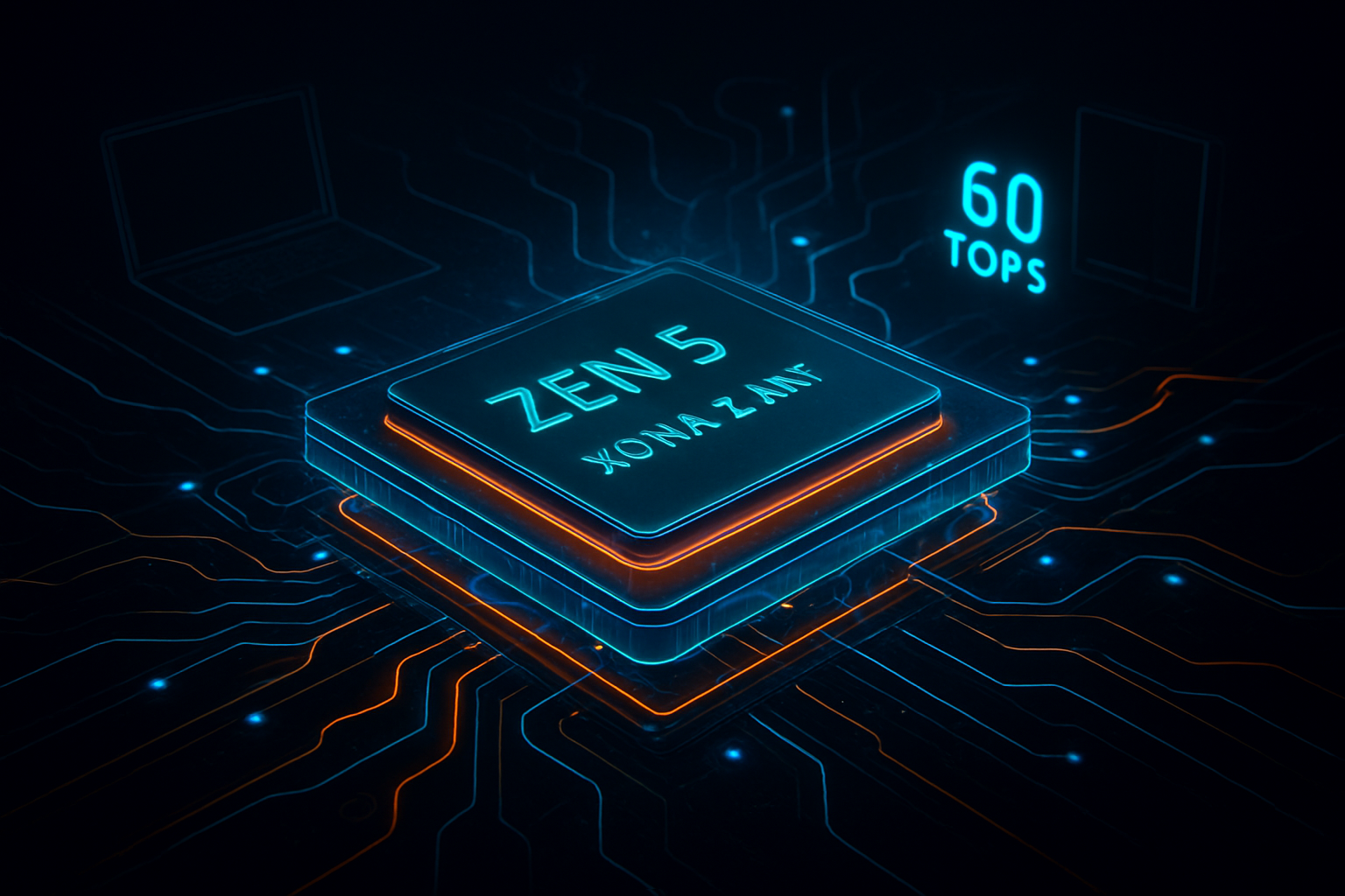
    The star of the show, the Ryzen AI 400 series (codenamed "Gorgon Point"), is built on a refined 4nm process and utilizes the Zen 5 microarchitecture. The flagship of this lineup, the Ryzen AI 9 HX 475, introduces the second-generation XDNA 2 NPU, which has been clocked to deliver a staggering 60 TOPS (Trillions of Operations Per Second). This marks a 20% increase over the previous generation and comfortably surpasses the 40-50 TOPS threshold required for the latest Microsoft Copilot+ features. This performance boost is achieved through a mix of high-performance Zen 5 cores and efficiency-focused Zen 5c cores, allowing thin-and-light laptops to maintain long battery life while processing complex AI tasks locally.

    For the professional and enthusiast market, the Ryzen AI Max series (codenamed "Strix Halo") pushes the boundaries of what integrated silicon can achieve. These chips, such as the Ryzen AI Max+ 392, feature up to 12 Zen 5 cores paired with a massive 40-core RDNA 3.5 integrated GPU. While the NPU in the Max series holds steady at 50 TOPS, its true power lies in its graphics-based AI compute—capable of up to 60 TFLOPS—and support for up to 128GB of LPDDR5X unified memory. This unified memory architecture is a direct response to the needs of AI developers, enabling the local execution of LLMs with up to 200 billion parameters, a feat previously impossible without high-end discrete graphics cards.

    This technical leap differs from previous approaches by focusing heavily on "balanced throughput." Rather than just chasing raw CPU clock speeds, AMD has optimized the interconnects between the Zen 5 cores, the RDNA 3.5 GPU, and the XDNA 2 NPU. Early reactions from industry experts suggest that AMD has successfully addressed the "memory bottleneck" that has plagued mobile AI performance. Analysts at the event noted that the ability to run massive models locally on a laptop-sized chip significantly reduces latency and enhances privacy, making these processors highly attractive for enterprise and creative workflows.

    Disrupting the Status Quo: A Direct Challenge to NVIDIA and Intel

    The introduction of the Ryzen AI Max series is a strategic shot across the bow for NVIDIA's workstation dominance. AMD explicitly positioned its new "Ryzen AI Halo" developer platforms as rivals to NVIDIA’s DGX Spark mini-workstations. By offering superior "tokens-per-second-per-dollar" for local LLM inference, AMD is targeting the growing demographic of AI researchers and developers who require powerful local hardware but may be priced out of NVIDIA’s high-end discrete GPU ecosystem. This competitive pressure could force a pricing realignment in the professional workstation market.

    Furthermore, AMD’s push into the edge and industrial sectors with the Ryzen AI Embedded P100 and X100 series directly challenges the NVIDIA Jetson lineup. These chips are designed for automotive digital cockpits and humanoid robotics, featuring industrial-grade temperature tolerances and a unified software stack. For tech giants like Tesla or robotics startups, the availability of a high-performance, X86-compatible alternative to ARM-based NVIDIA solutions provides more flexibility in software development and deployment.

    Major PC manufacturers, including Dell, HP, and Lenovo, have already announced dozens of designs based on the Ryzen AI 400 series. These companies stand to benefit from a renewed consumer interest in AI-capable hardware, potentially sparking a massive upgrade cycle. Meanwhile, Intel (NASDAQ: INTC) finds itself in a defensive position; while its "Panther Lake" chips offer competitive NPU performance, AMD’s lead in integrated graphics and unified memory for the workstation segment gives it a strategic advantage in the high-margin "Prosumer" market.

    The Broader AI Landscape: From Cloud to Edge

    AMD’s CES 2026 announcements reflect a broader trend in the AI landscape: the decentralization of intelligence. For the past several years, the "AI boom" has been characterized by massive data centers and cloud-based API calls. However, concerns over data privacy, latency, and the sheer cost of cloud compute have driven a demand for local execution. By delivering 60 TOPS in a thin-and-light form factor, AMD is making "Personal AI" a reality, where sensitive data never has to leave the user's device.

    This shift has profound implications for software development. With the release of ROCm 7.2, AMD is finally bringing its professional-grade AI software stack to the consumer and edge levels. This move aims to erode NVIDIA’s "CUDA moat" by providing an open-source, cross-platform alternative that works seamlessly across Windows and Linux. If AMD can successfully convince developers to optimize for ROCm at the edge, it could fundamentally change the power dynamics of the AI software ecosystem, which has been dominated by NVIDIA for over a decade.

    However, this transition is not without its challenges. The industry still lacks a unified standard for AI performance measurement, and "TOPS" can often be a misleading metric if the software cannot efficiently utilize the hardware. Comparisons to previous milestones, such as the transition to multi-core processing in the mid-2000s, suggest that we are currently in a "Wild West" phase of AI hardware, where architectural innovation is outpacing software standardization.

    The Horizon: What Lies Ahead for Ryzen AI

    Looking forward, the near-term focus for AMD will be the successful rollout of the Ryzen AI 400 series in Q1 2026. The real test will be the performance of these chips in real-world "Physical AI" applications. We expect to see a surge in specialized laptops and mini-PCs designed specifically for local AI training and "fine-tuning," where users can take a base model and customize it with their own data without needing a server farm.

    In the long term, the Ryzen AI Max series could pave the way for a new category of "AI-First" devices. Experts predict that by 2027, the distinction between a "laptop" and an "AI workstation" will blur, as unified memory architectures become the standard. The potential for these chips to power sophisticated humanoid robotics and autonomous vehicles is also on the horizon, provided AMD can maintain its momentum in the embedded space. The next major hurdle will be the integration of even more advanced "Agentic AI" capabilities directly into the silicon, allowing the NPU to proactively manage complex workflows without user intervention.

    Final Reflections on AMD’s AI Evolution

    AMD’s performance at CES 2026 marks a significant milestone in the company’s history. By successfully integrating Zen 5, RDNA 3.5, and XDNA 2 into a cohesive and powerful package, they have transitioned from a "CPU company" to a "Total AI Silicon company." The Ryzen AI 400 and Ryzen AI Max series are not just products; they are a statement of intent that AMD is ready to lead the charge into the era of pervasive, local artificial intelligence.

    The significance of this development in AI history lies in the democratization of high-performance compute. By bringing 60 TOPS and massive unified memory to the consumer and professional edge, AMD is lowering the barrier to entry for AI innovation. In the coming weeks and months, the tech world will be watching closely as the first Ryzen AI 400 systems hit the shelves and developers begin to push the limits of ROCm 7.2. The battle for the edge has officially begun, and AMD has just claimed a formidable piece of the high ground.


    This content is intended for informational purposes only and represents analysis of current AI developments.

    TokenRing AI delivers enterprise-grade solutions for multi-agent AI workflow orchestration, AI-powered development tools, and seamless remote collaboration platforms.
    For more information, visit https://www.tokenring.ai/.

  • The Rubin Era Begins: NVIDIA’s R100 “Vera Rubin” Architecture Enters Production with a 3x Leap in AI Density

    The Rubin Era Begins: NVIDIA’s R100 “Vera Rubin” Architecture Enters Production with a 3x Leap in AI Density

    As of early 2026, the artificial intelligence industry is bracing for its most significant hardware transition to date. NVIDIA (NASDAQ:NVDA) has officially confirmed that its next-generation "Vera Rubin" (R100) architecture has entered full-scale production, setting the stage for a massive commercial rollout in the second half of 2026. This announcement, detailed during the recent CES 2026 keynote, marks a pivotal shift in NVIDIA's roadmap as the company moves to an aggressive annual release cadence, effectively shortening the lifecycle of the previous Blackwell architecture to maintain its stranglehold on the generative AI market.

    The R100 platform is not merely an incremental update; it represents a fundamental re-architecting of the data center. By integrating the new Vera CPU—the successor to the Grace CPU—and pioneering the use of HBM4 memory, NVIDIA is promising a staggering 3x leap in compute density over the current Blackwell systems. This advancement is specifically designed to power the next frontier of "Agentic AI," where autonomous systems require massive reasoning and planning capabilities that exceed the throughput of today’s most advanced clusters.

    Breaking the Memory Wall: Technical Specs of the R100 and Vera CPU

    The heart of the Vera Rubin platform is a sophisticated chiplet-based design fabricated on TSMC’s (NYSE:TSM) enhanced 3nm (N3P) process node. This shift from the 4nm process used in Blackwell allows for a 20% increase in transistor density and significantly improved power efficiency. A single Rubin GPU is estimated to house approximately 333 billion transistors—a nearly 60% increase over its predecessor. However, the most critical breakthrough lies in the memory subsystem. Rubin is the first architecture to fully integrate HBM4 memory, utilizing 8 to 12 stacks to deliver a breathtaking 22 TB/s of memory bandwidth per socket. This 2.8x increase in bandwidth over Blackwell Ultra is intended to solve the "memory wall" that has long throttled the performance of trillion-parameter Large Language Models (LLMs).

    Complementing the GPU is the Vera CPU, which moves away from off-the-shelf designs to feature 88 custom "Olympus" cores built on the ARM (NASDAQ:ARM) v9.2-A architecture. Unlike traditional processors, Vera introduces "Spatial Multi-Threading," a technique that physically partitions core resources to support 176 simultaneous threads, doubling the data processing and compression performance of the previous Grace CPU. When combined into the Rubin NVL72 rack-scale system, the architecture delivers 3.6 Exaflops of FP4 performance. This represents a 3.3x leap in compute density compared to the Blackwell NVL72, allowing enterprises to pack the power of a modern supercomputer into a single data center row.

    The Competitive Gauntlet: AMD, Intel, and the Hyperscaler Pivot

    NVIDIA's aggressive production timeline for R100 arrives as competitors attempt to close the gap. AMD (NASDAQ:AMD) has positioned its Instinct MI400 series, specifically the MI455X, as a formidable challenger. Boasting a massive 432GB of HBM4—significantly higher than the Rubin R100’s 288GB—AMD is targeting memory-constrained "Mixture-of-Experts" (MoE) models. Meanwhile, Intel (NASDAQ:INTC) has undergone a strategic pivot, reportedly shelving the commercial release of Falcon Shores to focus on its "Jaguar Shores" architecture, slated for late 2026 on the Intel 18A node. This leaves NVIDIA and AMD in a two-horse race for the high-end training market for the remainder of the year.

    Despite NVIDIA’s dominance, major hyperscalers are increasingly diversifying their silicon portfolios to mitigate the high costs associated with NVIDIA hardware. Google (NASDAQ:GOOGL) has begun internal deployments of its TPU v7 "Ironwood," while Amazon (NASDAQ:AMZN) is scaling its Trainium3 chips across AWS regions. Microsoft (NASDAQ:MSFT) and Meta (NASDAQ:META) are also expanding their respective Maia and MTIA programs. However, industry analysts note that NVIDIA’s CUDA software moat and the sheer density of the Vera Rubin platform make it nearly impossible for these internal chips to replace NVIDIA for frontier model training. Most hyperscalers are adopting a hybrid approach: utilizing Rubin for the most demanding training tasks while offloading inference and internal workloads to their own custom ASICs.

    Beyond the Chip: The Macro Impact on AI Economics and Infrastructure

    The shift to the Rubin architecture carries profound implications for the economics of artificial intelligence. By delivering a 10x reduction in the cost per token, NVIDIA is making the deployment of "Agentic AI"—systems that can reason, plan, and execute multi-step tasks autonomously—commercially viable for the first time. Analysts predict that the R100's density leap will allow researchers to train a trillion-parameter model with four times fewer GPUs than were required during the Blackwell era. This efficiency is expected to accelerate the timeline for achieving Artificial General Intelligence (AGI) by lowering the hardware barriers that currently limit the scale of recursive self-improvement in AI models.

    However, this unprecedented density comes with a significant infrastructure challenge: cooling. The Vera Rubin NVL72 rack is so power-intensive that liquid cooling is no longer an option—it is a mandatory requirement. The platform utilizes a "warm-water" Direct Liquid Cooling (DLC) design capable of managing the heat generated by a 600kW rack. This necessitates a massive overhaul of global data center infrastructure, as legacy air-cooled facilities are physically unable to support the R100's thermal demands. This transition is expected to spark a multi-billion dollar boom in the data center cooling and power management sectors as providers race to retrofit their sites for the Rubin era.

    The Road to 2H 2026: Future Developments and the Annual Cadence

    Looking ahead, NVIDIA’s move to an annual release cycle suggests that the "Rubin Ultra" and the subsequent "Vera Rubin Next" architectures are already deep in the design phase. In the near term, the industry will be watching for the first "early access" benchmarks from Tier-1 cloud providers who are expected to receive initial Rubin samples in mid-2026. The integration of HBM4 is also expected to drive a supply chain squeeze, with SK Hynix (KRX:000660) and Samsung (KRX:005930) reportedly operating at maximum capacity to meet NVIDIA’s stringent performance requirements.

    The primary challenge facing NVIDIA in the coming months will be execution. Transitioning to 3nm chiplets and HBM4 simultaneously is a high-risk technical feat. Any delays in TSMC’s packaging yields or HBM4 validation could ripple through the entire AI sector, potentially stalling the progress of major labs like OpenAI and Anthropic. Furthermore, as the hardware becomes more powerful, the focus will likely shift toward "sovereign AI," with nations increasingly viewing Rubin-class clusters as essential national infrastructure, potentially leading to further geopolitical tensions over export controls.

    A New Benchmark for the Intelligence Age

    The production of the Vera Rubin architecture marks a watershed moment in the history of computing. By delivering a 3x leap in density and nearly 4 Exaflops of performance in a single rack, NVIDIA has effectively redefined the ceiling of what is possible in AI research. The integration of the custom Vera CPU and HBM4 memory signals NVIDIA’s transformation from a GPU manufacturer into a full-stack data center company, capable of orchestrating every aspect of the AI workflow from the silicon to the interconnect.

    As we move toward the 2H 2026 launch, the industry's focus will remain on the real-world performance of these systems. If NVIDIA can deliver on its promises of a 10x reduction in token costs and a 5x boost in inference throughput, the "Rubin Era" will likely be remembered as the period when AI moved from a novelty into a ubiquitous, autonomous layer of the global economy. For now, the tech world waits for the fall of 2026, when the first Vera Rubin clusters will finally go online and begin the work of training the world's most advanced intelligence.


    This content is intended for informational purposes only and represents analysis of current AI developments.

    TokenRing AI delivers enterprise-grade solutions for multi-agent AI workflow orchestration, AI-powered development tools, and seamless remote collaboration platforms.
    For more information, visit https://www.tokenring.ai/.

  • The Angstrom Era Begins: Intel Completes Acceptance Testing of ASML’s $400M High-NA EUV Machine for 1.4nm Dominance

    The Angstrom Era Begins: Intel Completes Acceptance Testing of ASML’s $400M High-NA EUV Machine for 1.4nm Dominance

    In a landmark moment for the semiconductor industry, Intel (NASDAQ: INTC) has officially announced the successful completion of acceptance testing for ASML’s (NASDAQ: ASML) TWINSCAN EXE:5200B, the world’s most advanced High-Numerical Aperture (High-NA) Extreme Ultraviolet (EUV) lithography system. This milestone, finalized in early January 2026, signals the transition of High-NA technology from experimental pilot programs into a production-ready state. By validating the performance of this $400 million machine, Intel has effectively fired the starting gun for the "Angstrom Era," a new epoch of chip manufacturing defined by features measured at the sub-2-nanometer scale.

    The completion of these tests at Intel’s D1X facility in Oregon represents a massive strategic bet by the American chipmaker to reclaim the crown of process leadership. With the EXE:5200B now fully operational and under Intel Foundry’s control, the company is moving aggressively toward the development of its Intel 14A (1.4nm) node. This development is not merely a technical upgrade; it is a foundational shift in how the world’s most complex silicon—particularly the high-performance processors required for generative AI—will be designed and manufactured over the next decade.

    Technical Mastery: The EXE:5200B and the Physics of 1.4nm

    The ASML EXE:5200B represents a quantum leap over standard EUV systems by increasing the Numerical Aperture (NA) from 0.33 to 0.55. This change in optics allows the machine to project much finer patterns onto silicon wafers, achieving a resolution of 8nm in a single exposure. This is a critical departure from previous methods where manufacturers had to rely on "double-patterning"—a time-consuming and error-prone process of splitting a single layer's design across two masks. By utilizing High-NA EUV, Intel can achieve the necessary precision for the 14A node with single-patterning, significantly reducing manufacturing complexity and improving potential yields.

    During the recently concluded acceptance testing, the EXE:5200B met or exceeded all critical performance benchmarks required for high-volume manufacturing (HVM). Most notably, the system demonstrated a throughput of 175 to 220 wafers per hour, a substantial improvement over the 185 wph limit of the earlier EXE:5000 pilot system. Furthermore, the machine achieved an overlay precision of 0.7 nanometers, a level of accuracy equivalent to aligning two objects with the width of a few atoms across a distance of several miles. This precision is essential for the 14A node, which integrates Intel’s second-generation "PowerDirect" backside power delivery and refined RibbonFET (Gate-All-Around) transistors.

    The reaction from the semiconductor research community has been one of cautious optimism mixed with awe at the engineering feat. Industry experts note that while the $400 million price tag per unit is staggering, the reduction in mask steps and the ability to print features at the 1.4nm scale are the only viable paths forward as the industry hits the physical limits of light-based lithography. The successful validation of the EXE:5200B proves that the industry’s roadmap toward the 10-Angstrom (1nm) threshold is no longer a theoretical exercise but a mechanical reality.

    A New Competitive Front: Intel vs. The World

    The operationalization of High-NA EUV creates a stark divergence in the strategies of the world’s leading foundries. While Intel has moved "all-in" on High-NA to leapfrog its competitors, Taiwan Semiconductor Manufacturing Company (NYSE: TSM) has maintained a more conservative stance. TSMC has indicated it will continue to push standard 0.33 NA EUV to its limits for its own 1.4nm-class (A14) nodes, likely relying on complex multi-patterning techniques. This gives Intel a narrow but significant window to establish a "High-NA lead," potentially offering better cycle times and lower defect rates for the next generation of AI chips.

    For AI giants and fabless designers like NVIDIA (NASDAQ: NVDA) and Apple (NASDAQ: AAPL), Intel’s progress is a welcome development that could provide a much-needed alternative to TSMC’s currently oversubscribed capacity. Intel Foundry has already released the Process Design Kit (PDK) 1.0 for the 14A node to early customers, allowing them to begin the multi-year design process for chips that will eventually run on the EXE:5200B. If Intel can translate this hardware advantage into stable, high-yield production, it could disrupt the current foundry hierarchy and regain the strategic advantage it lost over the last decade.

    However, the stakes are equally high for the startups and mid-tier players in the AI space. The extreme cost of High-NA lithography—both in terms of the machines themselves and the design complexity of 1.4nm chips—threatens to create a "compute divide." Only the most well-capitalized firms will be able to afford the multi-billion dollar design costs associated with the Angstrom Era. This could lead to further market consolidation, where a handful of tech titans control the most advanced hardware, while others are left to innovate on older, more affordable nodes like 18A or 3nm.

    Moore’s Law and the Geopolitics of Silicon

    The arrival of the EXE:5200B is a powerful rebuttal to those who have long predicted the death of Moore’s Law. By successfully shrinking features below the 2nm barrier, Intel and ASML have demonstrated that the "treadmill" of semiconductor scaling still has several generations of life left. This is particularly significant for the broader AI landscape; as large language models (LLMs) grow in complexity, the demand for more transistors per square millimeter and better power efficiency becomes an existential requirement for the industry’s growth.

    Beyond the technical achievements, the deployment of these machines has profound geopolitical and economic implications. The $400 million cost per machine, combined with the billions required for the cleanrooms that house them, makes advanced chipmaking one of the most capital-intensive endeavors in human history. With Intel’s primary High-NA site located in Oregon, the United States is positioning itself as a central hub for the most advanced manufacturing on the planet. This aligns with broader national security goals to secure the supply chain for the chips that power everything from autonomous defense systems to the future of global finance.

    However, the sheer scale of this investment raises concerns about the sustainability of the "smaller is better" race. The energy requirements of EUV lithography are immense, and the complexity of the supply chain—where a single company, ASML, is the sole provider of the necessary hardware—creates a single point of failure for the entire global tech economy. As we enter the Angstrom Era, the industry must balance its drive for performance with the reality of these economic and environmental costs.

    The Road to 10A: What Lies Ahead

    Looking toward the near term, the focus now shifts from acceptance testing to "risk production." Intel expects to begin risk production on the 14A node by late 2026, with high-volume manufacturing (HVM) targeted for the 2027–2028 timeframe. During this period, the company will need to refine the integration of High-NA EUV with its other "Angstrom-ready" technologies, such as the PowerDirect backside power delivery system, which moves power lines to the back of the wafer to free up space for signals on the front.

    The long-term roadmap is even more ambitious. The lessons learned from the EXE:5200B will pave the way for the Intel 10A (1nm) node, which is expected to debut toward the end of the decade. Experts predict that the next few years will see a flurry of innovation in "chiplet" architectures and advanced packaging, as manufacturers look for ways to augment the gains provided by High-NA lithography. The challenge will be managing the heat and power density of chips that pack billions of transistors into a space the size of a fingernail.

    Predicting the exact impact of 1.4nm silicon is difficult, but the potential applications are transformative. We are looking at a future where on-device AI can handle tasks currently reserved for massive data centers, where medical devices can perform real-time genomic sequencing, and where the energy efficiency of global compute infrastructure finally begins to keep pace with its expanding scale. The hurdles remain significant—particularly in terms of software optimization and the cooling of these ultra-dense chips—but the hardware foundation is now being laid.

    A Milestone in the History of Computing

    The completion of acceptance testing for the ASML EXE:5200B marks a definitive turning point in the history of artificial intelligence and computing. It represents the successful navigation of one of the most difficult engineering challenges ever faced by the semiconductor industry: moving beyond the limits of standard EUV to enter the Angstrom Era. For Intel, it is a "make or break" moment that validates their aggressive roadmap and places them at the forefront of the next generation of silicon manufacturing.

    As we move through 2026, the industry will be watching closely for the first "first-light" chips from the 14A node and the subsequent performance data. The success of this $400 million technology will ultimately be measured by the capabilities of the AI models it powers and the efficiency of the devices it inhabits. For now, the message is clear: the race to the bottom of the nanometer scale has reached a new, high-velocity phase, and the era of 1.4nm dominance has officially begun.


    This content is intended for informational purposes only and represents analysis of current AI developments.

    TokenRing AI delivers enterprise-grade solutions for multi-agent AI workflow orchestration, AI-powered development tools, and seamless remote collaboration platforms.
    For more information, visit https://www.tokenring.ai/.

  • Intel Reclaims the Silicon Crown: Core Ultra Series 3 “Panther Lake” Debuts at CES 2026

    Intel Reclaims the Silicon Crown: Core Ultra Series 3 “Panther Lake” Debuts at CES 2026

    LAS VEGAS — In a landmark moment for the American semiconductor industry, Intel (NASDAQ: INTC) officially launched its Core Ultra Series 3 processors, codenamed "Panther Lake," at CES 2026. This release marks the first consumer platform built on the highly anticipated Intel 18A process, representing the culmination of CEO Pat Gelsinger’s "five nodes in four years" strategy and a bold bid to regain undisputed process leadership from global rivals.

    The announcement is being hailed as a watershed event for both the AI PC market and domestic manufacturing. By bringing the world’s most advanced semiconductor process to high-volume production on U.S. soil, Intel is not just launching a new chip; it is attempting to shift the center of gravity for the global tech supply chain back to North America.

    The Engineering Marvel of 18A: RibbonFET and PowerVia

    Panther Lake is defined by its underlying manufacturing technology, Intel 18A, which introduces two foundational innovations to the market for the first time. The first is RibbonFET, Intel’s implementation of Gate-All-Around (GAA) transistor architecture. Unlike the FinFET designs that have dominated the industry for a decade, RibbonFET wraps the gate entirely around the channel, providing superior electrostatic control and significantly reducing power leakage. This allows for faster switching speeds in a smaller footprint, which Intel claims delivers a 15% performance-per-watt improvement over its predecessor.

    The second, and perhaps more revolutionary, innovation is PowerVia. This is the industry’s first implementation of backside power delivery, a technique that moves the power routing from the top of the silicon wafer to the bottom. By separating power and signal wires, Intel has eliminated the "wiring congestion" that has plagued chip designers for years. Initial benchmarks suggest this architectural shift improves cell utilization by nearly 10%, allowing the Core Ultra Series 3 to sustain higher clock speeds without the thermal throttling seen in previous generations.

    On the AI front, Panther Lake introduces the NPU 5 architecture, a dedicated neural processing unit capable of 50 Trillion Operations Per Second (TOPS). When combined with the new Xe3 "Celestial" graphics tiles and the high-performance CPU cores, the total platform throughput reaches a staggering 180 TOPS. This level of local compute power enables real-time execution of complex Vision-Language-Action (VLA) models and large language models (LLMs) like Llama 3 directly on the device, reducing the need for cloud-based AI processing and enhancing user privacy.

    A New Competitive Front in the Silicon Wars

    The launch of Panther Lake sets the stage for a brutal confrontation with Taiwan Semiconductor Manufacturing Company (NYSE: TSM). While TSMC is also ramping up its 2nm (N2) process, Intel's 18A is the first to market with backside power delivery—a feature TSMC isn't expected to implement in high volume until its N2P node later in 2026 or 2027. This technical head-start gives Intel a strategic window to court major fabless customers who are looking for the most efficient AI silicon.

    For competitors like Advanced Micro Devices (NASDAQ: AMD) and Qualcomm (NASDAQ: QCOM), the pressure is mounting. AMD’s upcoming Zen 6 architecture and Qualcomm’s next-generation Snapdragon X Elite chips will now be measured against the efficiency gains of Intel’s PowerVia. Furthermore, the massive 77% leap in gaming performance provided by Intel's Xe3 graphics architecture threatens to disrupt the low-to-midrange discrete GPU market, potentially impacting NVIDIA (NASDAQ: NVDA) as integrated graphics become "good enough" for the majority of mainstream gamers and creators.

    Market analysts suggest that Intel’s aggressive move into the 1.8nm-class era is as much about its foundry business as it is about its own chips. By proving that 18A can yield high-performance consumer silicon at scale, Intel is sending a clear signal to potential foundry customers like Microsoft (NASDAQ: MSFT) and Amazon (NASDAQ: AMZN) that it is a viable, cutting-edge alternative to TSMC for their custom AI accelerators.

    The Geopolitical and Economic Significance of U.S. Manufacturing

    Beyond the specs, the "Made in USA" badge on Panther Lake carries immense weight. The compute tiles for the Core Ultra Series 3 are being manufactured at Fab 52 in Chandler, Arizona, with advanced packaging taking place in Rio Rancho, New Mexico. This makes Panther Lake the most advanced semiconductor product ever mass-produced in the United States, a feat supported by significant investment and incentives from the CHIPS and Science Act.

    This domestic manufacturing capability addresses growing concerns over supply chain resilience and the concentration of advanced chipmaking in East Asia. For the U.S. government and domestic tech giants, Intel 18A represents a critical step toward "technological sovereignty." However, the transition has not been without its critics. Some industry observers point out that while the compute tiles are domestic, Intel still relies on TSMC for certain GPU and I/O tiles in the Panther Lake "disaggregated" design, highlighting the persistent interconnectedness of the global semiconductor industry.

    The broader AI landscape is also shifting. As "AI PCs" become the standard rather than the exception, the focus is moving away from raw TOPS and toward "TOPS-per-watt." Intel’s claim of 27-hour battery life in premium ultrabooks suggests that the 18A process has finally solved the efficiency puzzle that allowed Apple (NASDAQ: AAPL) and its ARM-based silicon to dominate the laptop market for the past several years.

    Looking Ahead: The Road to 14A and Beyond

    While Panther Lake is the star of CES 2026, Intel is already looking toward the horizon. The company has confirmed that its next-generation server chip, Clearwater Forest, is already in the sampling phase on 18A, and the successor to Panther Lake—codenamed Nova Lake—is expected to push the boundaries of AI integration even further in 2027.

    The next major milestone will be the transition to Intel 14A, which will introduce High-Numerical Aperture (High-NA) EUV lithography. This will be the next great battlefield in the quest for "Angstrom-era" silicon. The primary challenge for Intel moving forward will be maintaining high yields on these increasingly complex nodes. If the 18A ramp stays on track, experts predict Intel could regain the crown for the highest-performing transistors in the industry by the end of the year, a position it hasn't held since the mid-2010s.

    A Turning Point for the Silicon Giant

    The launch of the Core Ultra Series 3 "Panther Lake" is more than just a product refresh; it is a declaration of intent. By successfully deploying RibbonFET and PowerVia on the 18A node, Intel has demonstrated that it can still innovate at the bleeding edge of physics. The 180 TOPS of AI performance and the promise of "all-day-plus" battery life position the AI PC as the central tool for the next decade of productivity.

    As the first units begin shipping to consumers on January 27, the industry will be watching closely to see if Intel can translate this technical lead into market share gains. For now, the message from Las Vegas is clear: the silicon crown is back in play, and for the first time in a generation, the most advanced chips in the world are being forged in the American desert.


    This content is intended for informational purposes only and represents analysis of current AI developments.

    TokenRing AI delivers enterprise-grade solutions for multi-agent AI workflow orchestration, AI-powered development tools, and seamless remote collaboration platforms.
    For more information, visit https://www.tokenring.ai/.

  • TSMC Enters the 2nm Era: A New Dawn for AI Supremacy as Volume Production Begins

    TSMC Enters the 2nm Era: A New Dawn for AI Supremacy as Volume Production Begins

    As the calendar turns to early 2026, the global semiconductor landscape has reached a pivotal inflection point. Taiwan Semiconductor Manufacturing Company (TSM:NYSE), the world’s largest contract chipmaker, has officially commenced volume production of its highly anticipated 2-nanometer (N2) process node. This milestone, centered at the company’s massive Fab 20 in Hsinchu and the newly repurposed Fab 22 in Kaohsiung, marks the first time the industry has transitioned away from the long-standing FinFET transistor architecture to the revolutionary Gate-All-Around (GAA) nanosheet technology.

    The immediate significance of this development cannot be overstated. With initial yield rates reportedly exceeding 65%—a remarkably high figure for a first-generation architectural shift—TSMC is positioning itself to capture an unprecedented 95% of the AI accelerator market. As AI demand continues to surge across every sector of the global economy, the 2nm node is no longer just a technical upgrade; it is the essential bedrock for the next generation of large language models, autonomous systems, and "Physical AI" applications.

    The Nanosheet Revolution: Inside the N2 Architecture

    The transition to the N2 node represents the most significant architectural change in chip manufacturing in over a decade. By moving from FinFET to GAAFET (Gate-All-Around Field-Effect Transistor) nanosheet technology, TSMC has effectively re-engineered how electrons flow through a chip. In this new design, the gate surrounds the channel on all four sides, providing superior electrostatic control, drastically reducing current leakage, and allowing for much finer tuning of performance and power consumption.

    Technically, the N2 node delivers a substantial leap over the previous 3nm (N3E) generation. According to official specifications, the new process offers a 10% to 15% increase in processing speed at the same power level, or a staggering 25% to 30% reduction in power consumption at the same speed. Furthermore, logic density has seen a boost of approximately 15%, allowing designers to pack more transistors into the same footprint. This is complemented by TSMC’s "Nano-Flex" technology, which allows chip designers to mix different nanosheet heights within a single block to optimize for either extreme performance or ultra-low power.

    Initial reactions from the AI research community and industry experts have been overwhelmingly positive. Analysts at JPMorgan (JPM:NYSE) and Goldman Sachs (GS:NYSE) have characterized the N2 launch as the start of a "multi-year AI supercycle." The industry is particularly impressed by the maturity of the ecosystem; unlike previous node transitions that faced years of delay, TSMC’s 2nm ramp-up has met every internal milestone, providing a stable foundation for the world's most complex silicon designs.

    A 1.5x Surge in Tape-Outs: The Strategic Advantage for Tech Giants

    The business impact of the 2nm node is already visible in the sheer volume of customer engagement. Reports indicate that the N2 family has recorded 1.5 times more "tape-outs"—the final stage of the design process before manufacturing—than the 3nm node did at the same point in its lifecycle. This surge is driven by a unique convergence: for the first time, mobile giants like Apple (AAPL:NASDAQ) and high-performance computing (HPC) leaders like NVIDIA (NVDA:NASDAQ) and Advanced Micro Devices (AMD:NASDAQ) are racing for the same leading-edge capacity simultaneously.

    AMD has notably used the 2nm transition to execute a strategic "leapfrog" over its competitors. At CES 2026, Dr. Lisa Su confirmed that the new Instinct MI400 series AI accelerators are built on TSMC’s N2 process, whereas NVIDIA's recently unveiled "Vera Rubin" architecture utilizes an enhanced 3nm (N3P) node. This gives AMD a temporary edge in raw transistor density and energy efficiency, particularly for memory-intensive LLM training. Meanwhile, Apple has secured over 50% of the initial 2nm capacity for its upcoming A20 chips, ensuring that the next generation of iPhones will maintain a significant lead in on-device AI processing.

    The competitive implications for other foundries are stark. While Intel (INTC:NASDAQ) is pushing its 18A node and Samsung (SSNLF:OTC) is refining its own GAA process, TSMC’s 95% projected market share in AI accelerators suggests a widening "foundry gap." TSMC’s moat is not just the silicon itself, but its advanced packaging ecosystem, specifically CoWoS (Chip on Wafer on Substrate), which is essential for the multi-die configurations used in modern AI GPUs.

    Silicon Sovereignty and the Broader AI Landscape

    The successful ramp of 2nm production at Fab 20 and Fab 22 carries immense weight in the broader context of "Silicon Sovereignty." As nations race to secure their AI supply chains, TSMC’s ability to deliver 2nm at scale reinforces Taiwan's position as the indispensable hub of the global tech economy. This development fits into a larger trend where the bottleneck for AI progress has shifted from software algorithms to the physical availability of advanced silicon and the energy required to run it.

    The power efficiency gains of the N2 node—up to 30%—are perhaps its most critical contribution to the AI landscape. With data centers consuming an ever-growing share of the world’s electricity, the ability to perform more "tokens per watt" is the only sustainable path forward for the AI industry. Comparisons are already being made to the 7nm breakthrough of 2018, which enabled the first wave of modern mobile computing; however, the 2nm era is expected to have a far more profound impact on infrastructure, enabling the transition from cloud-based AI to ubiquitous, "always-on" intelligence in edge devices and robotics.

    However, this concentration of power also raises concerns. The projected 95% market share for AI accelerators creates a single point of failure for the global AI economy. Any disruption to TSMC’s 2nm production lines could stall the progress of thousands of AI startups and tech giants alike. This has led to intensified efforts by hyperscalers like Amazon (AMZN:NASDAQ), Google (GOOGL:NASDAQ), and Microsoft (MSFT:NASDAQ) to design their own custom AI ASICs on N2, attempting to gain some measure of control over their hardware destinies.

    The Road to 1.4nm and Beyond: What’s Next for TSMC?

    Looking ahead, the 2nm node is merely the first chapter in a new book of semiconductor physics. TSMC has already outlined its roadmap for the second half of 2026, which includes the N2P (performance-enhanced) node and the introduction of the A16 (1.6-nanometer) process. The A16 node will be the first to feature Backside Power Delivery (BSPD), a technique that moves the power wiring to the back of the wafer to further improve efficiency and signal integrity.

    Experts predict that the primary challenge moving forward will be the integration of these advanced chips with next-generation memory, such as HBM4. As chip density increases, the "memory wall"—the gap between processor speed and memory bandwidth—becomes the new limiting factor. We can expect to see TSMC deepen its partnerships with memory leaders like SK Hynix and Micron (MU:NASDAQ) to create integrated 3D-stacked solutions that blur the line between logic and memory.

    In the long term, the focus will shift toward the A14 node (1.4nm), currently slated for 2027-2028. The industry is watching closely to see if the nanosheet architecture can be scaled that far, or if entirely new materials, such as carbon nanotubes or two-dimensional semiconductors, will be required. For now, the successful execution of N2 provides a clear runway for the next three years of AI innovation.

    Conclusion: A Landmark Moment in Computing History

    The commencement of 2nm volume production in early 2026 is a landmark achievement that cements TSMC’s dominance in the semiconductor industry. By successfully navigating the transition to GAA nanosheet technology and securing a massive 1.5x surge in tape-outs, the company has effectively decoupled itself from the traditional cycles of the chip market, becoming an essential utility for the AI era.

    The key takeaway for the coming months is the rapid shift in the competitive landscape. With AMD and Apple leading the charge onto 2nm, the pressure is now on NVIDIA and Intel to prove that their architectural innovations can compensate for a lag in process technology. Investors and industry watchers should keep a close eye on the output levels of Fab 20 and Fab 22; their success will determine the pace of AI advancement for the remainder of the decade. As we look toward the mid-2020s, it is clear that the 2nm era is not just about smaller transistors—it is about the limitless potential of the silicon that powers our world.


    This content is intended for informational purposes only and represents analysis of current AI developments.

    TokenRing AI delivers enterprise-grade solutions for multi-agent AI workflow orchestration, AI-powered development tools, and seamless remote collaboration platforms.
    For more information, visit https://www.tokenring.ai/.

  • The Dawn of the AI Factory: NVIDIA Blackwell B200 Enters Full Production as Naver Scales Korea’s Largest AI Cluster

    The Dawn of the AI Factory: NVIDIA Blackwell B200 Enters Full Production as Naver Scales Korea’s Largest AI Cluster

    SANTA CLARA, CA — January 8, 2026 — The global landscape of artificial intelligence has reached a definitive turning point as NVIDIA (NASDAQ:NVDA) announced today that its Blackwell B200 architecture has entered full-scale volume production. This milestone marks the transition of the world’s most powerful AI chip from early-access trials to the backbone of global industrial intelligence. With supply chain bottlenecks for critical components like High Bandwidth Memory (HBM3e) and advanced packaging finally stabilizing, NVIDIA is now shipping Blackwell units in the tens of thousands per week, effectively sold out through mid-2026.

    The significance of this production ramp-up was underscored by South Korean tech titan Naver (KRX:035420), which recently completed the deployment of Korea’s largest AI computing cluster. Utilizing 4,000 Blackwell B200 GPUs, the "B200 4K Cluster" is designed to propel the next generation of "omni models"—systems capable of processing text, video, and audio simultaneously. Naver’s move signals a broader shift toward "AI Sovereignty," where nations and regional giants build massive, localized infrastructure to maintain a competitive edge in the era of trillion-parameter models.

    Redefining the Limits of Silicon: The Blackwell Architecture

    The Blackwell B200 is not merely an incremental upgrade; it represents a fundamental architectural shift from its predecessor, the H100 (Hopper). While the H100 was a monolithic chip, the B200 utilizes a revolutionary chiplet-based design, connecting two reticle-limited dies via a 10 TB/s ultra-high-speed link. This allows the 208 billion transistors to function as a single unified processor, effectively bypassing the physical limits of traditional silicon manufacturing. The B200 boasts 192GB of HBM3e memory and 8 TB/s of bandwidth, more than doubling the capacity and speed of previous generations.

    A key differentiator in the Blackwell era is the introduction of FP4 (4-bit floating point) precision. This technical leap, managed by a second-generation Transformer Engine, allows the B200 to process trillion-parameter models with 30 times the inference throughput of the H100. This capability is critical for the industry's pivot toward Mixture-of-Experts (MoE) models, where only a fraction of the model’s parameters are active at any given time, drastically reducing the energy cost per token. Initial reactions from the research community suggest that Blackwell has "reset the scaling laws," enabling real-time reasoning for models that were previously too large to serve efficiently.

    The "AI Factory" Era and the Corporate Arms Race

    NVIDIA CEO Jensen Huang has frequently described this transition as the birth of the "AI Factory." In this paradigm, data centers are no longer viewed as passive storage hubs but as industrial facilities where raw data is the raw material and "intelligence" is the finished product. This shift is visible in the strategic moves of hyperscalers and sovereign nations alike. While Naver is leading the charge in South Korea, global giants like Microsoft (NASDAQ:MSFT), Amazon (NASDAQ:AMZN), and Alphabet (NASDAQ:GOOGL) are integrating Blackwell into their clouds to support massive agentic systems—AI that doesn't just chat, but autonomously executes multi-step tasks.

    However, NVIDIA is not without challengers. As Blackwell hits full production, AMD (NASDAQ:AMD) has countered with its MI350 and MI400 series, the latter featuring up to 432GB of HBM4 memory. Meanwhile, Google has ramped up its TPU v7 "Ironwood" chips, and Amazon’s Trainium3 is gaining traction among startups looking for a lower "Nvidia Tax." These competitors are focusing on "Total Cost of Ownership" (TCO) and energy efficiency, aiming to capture the 30-40% of internal workloads that hyperscalers are increasingly moving toward custom silicon. Despite this, NVIDIA’s software moat—CUDA—and the sheer scale of the Blackwell rollout keep it firmly in the lead.

    Global Implications and the Sovereign AI Trend

    The deployment of the Blackwell architecture fits into a broader trend of "Sovereign AI," where countries recognize that AI capacity is as vital as energy or food security. Naver’s 4,000-GPU cluster is a prime example of this, providing South Korea with the computational self-reliance to develop foundation models like HyperCLOVA X without total dependence on Silicon Valley. Naver CEO Choi Soo-yeon noted that training tasks that previously took 18 months can now be completed in just six weeks, a 12-fold acceleration that fundamentally changes the pace of national innovation.

    Yet, this massive scaling brings significant concerns, primarily regarding energy consumption. A single GB200 NVL72 rack—a cluster of 72 Blackwell GPUs acting as one—can draw over 120kW of power, necessitating a mandatory shift toward liquid cooling solutions. The industry is now grappling with the "Energy Wall," leading to unprecedented investments in modular nuclear reactors and specialized power grids to sustain these AI factories. This has turned the AI race into a competition not just for chips, but for the very infrastructure required to keep them running.

    The Horizon: From Reasoning to Agency

    Looking ahead, the full production of Blackwell is expected to catalyze the move from "Reasoning AI" to "Agentic AI." Near-term developments will likely see the rise of autonomous systems capable of managing complex logistics, scientific discovery, and software development with minimal human oversight. Experts predict that the next 12 to 24 months will see the emergence of models exceeding 10 trillion parameters, powered by the Blackwell B200 and its already-announced successor, the Blackwell Ultra (B300), and the future "Rubin" (R100) architecture.

    The challenges remaining are largely operational and ethical. As AI factories begin producing "intelligence" at an industrial scale, the industry must address the environmental impact of such massive compute and the societal implications of increasingly autonomous agents. However, the momentum is undeniable. OpenAI CEO Sam Altman recently remarked that there is "no scaling wall" in sight, and the massive Blackwell deployment in early 2026 appears to validate that conviction.

    A New Chapter in Computing History

    In summary, the transition of the NVIDIA Blackwell B200 into full production is a landmark event that formalizes the "AI Factory" as the central infrastructure of the 21st century. With Naver’s massive cluster serving as a blueprint for national AI sovereignty and the B200’s technical specs pushing the boundaries of what is computationally possible, the industry has moved beyond the experimental phase of generative AI.

    As we move further into 2026, the focus will shift from the availability of chips to the efficiency of the factories they power. The coming months will be defined by how effectively companies and nations can translate this unprecedented raw compute into tangible economic and scientific breakthroughs. For now, the Blackwell era has officially begun, and the world is only starting to see the scale of the intelligence it will produce.


    This content is intended for informational purposes only and represents analysis of current AI developments.

    TokenRing AI delivers enterprise-grade solutions for multi-agent AI workflow orchestration, AI-powered development tools, and seamless remote collaboration platforms.
    For more information, visit https://www.tokenring.ai/.

  • The Great Decoupling: How Hyperscalers are Breaking NVIDIA’s Iron Grip with Custom Silicon

    The Great Decoupling: How Hyperscalers are Breaking NVIDIA’s Iron Grip with Custom Silicon

    The era of the general-purpose AI chip is rapidly giving way to a new age of hyper-specialization. As of early 2026, the world’s largest cloud providers—Google (NASDAQ:GOOGL), Amazon (NASDAQ:AMZN), and Microsoft (NASDAQ:MSFT)—have fundamentally rewritten the rules of the AI infrastructure market. By designing their own custom silicon, these "hyperscalers" are no longer just customers of the semiconductor industry; they are its most formidable architects. This strategic shift, often referred to as the "Silicon Divorce," marks a pivotal moment where the software giants have realized that to own the future of artificial intelligence, they must first own the atoms that power it.

    The immediate significance of this transition cannot be overstated. By moving away from a one-size-fits-all hardware model, these companies are slashing the astronomical "NVIDIA tax," reducing energy consumption in an increasingly power-constrained world, and optimizing their hardware for the specific nuances of their multi-trillion-parameter models. This vertical integration—controlling everything from the power source to the chip architecture to the final AI agent—is creating a competitive moat that is becoming nearly impossible for smaller players to cross.

    The Rise of the AI ASIC: Technical Frontiers of 2026

    The technical landscape of 2026 is dominated by Application-Specific Integrated Circuits (ASICs) that leave traditional GPUs in the rearview mirror for specific AI tasks. Google’s latest offering, the TPU v7 (codenamed "Ironwood"), represents the pinnacle of this evolution. Utilizing a cutting-edge 3nm process from TSMC, the TPU v7 delivers a staggering 4.6 PFLOPS of dense FP8 compute per chip. Unlike general-purpose GPUs, Google uses Optical Circuit Switching (OCS) to dynamically reconfigure its "Superpods," allowing for 10x faster collective operations than equivalent Ethernet-based clusters. This architecture is specifically tuned for the massive KV-caches required for the long-context windows of Gemini 2.0 and beyond.

    Amazon has followed a similar path with its Trainium3 chip, which entered volume production in early 2026. Designed by Amazon’s Annapurna Labs, Trainium3 is the company's first 3nm-class chip, offering 2.5 PFLOPS of MXFP8 performance. Amazon’s strategy focuses on "price-performance," leveraging the Neuron SDK to allow developers to seamlessly switch from NVIDIA (NASDAQ:NVDA) hardware to custom silicon. Meanwhile, Microsoft has solidified its position with the Maia 2 (Braga) accelerator. While Maia 100 was a conservative first step, Maia 2 is a vertically integrated powerhouse designed specifically to run Azure OpenAI services like GPT-5 and Microsoft Copilot with maximum efficiency, utilizing custom Ethernet-based interconnects to bypass traditional networking bottlenecks.

    These advancements differ from previous approaches by stripping away legacy hardware components—such as graphics rendering units and 64-bit precision—that are unnecessary for AI workloads. This "lean" architecture allows for significantly higher transistor density dedicated solely to matrix multiplications. Initial reactions from the research community have been overwhelmingly positive, with many noting that the specialized memory hierarchies of these chips are the only reason we have been able to scale context windows into the tens of millions of tokens without a total collapse in inference speed.

    The Strategic Divorce: A New Power Dynamic in Silicon Valley

    This shift has created a seismic ripple across the tech industry, benefiting a new class of "silent partners." While the hyperscalers design the chips, they rely on specialized design firms like Broadcom (NASDAQ:AVGO) and Marvell (NASDAQ:MRVL) to bring them to life. Broadcom, which now commands nearly 70% of the custom AI ASIC market, has become the backbone of the "Silicon Divorce," serving as the primary design partner for both Google and Meta (NASDAQ:META). Marvell has similarly positioned itself as a "growth challenger," securing massive wins with Amazon and Microsoft by integrating advanced "Photonic Fabrics" that allow for ultra-fast chip-to-chip communication.

    For NVIDIA, the competitive implications are complex. While the company remains the market leader with its newly launched Vera Rubin architecture, it is no longer the only game in town. The "NVIDIA Tax"—the high margins associated with the H100 and B200 series—is being eroded by the hyperscalers' internal alternatives. In response, cloud pricing has shifted to a two-tier model. Hyperscalers now offer their internal chips at a 30% to 50% discount compared to NVIDIA-based instances, effectively using their custom silicon as a loss leader to lock enterprises into their respective cloud ecosystems.

    Startups and smaller AI labs are the unexpected beneficiaries of this hardware war. The increased availability of lower-cost, high-performance compute on platforms like AWS Trainium and Google TPU v7 has lowered the barrier to entry for training mid-sized foundation models. However, the strategic advantage remains with the giants; by co-designing the hardware and the software (such as Google’s XLA compiler or Amazon’s Triton integration), these companies can squeeze performance out of their chips that no third-party user can ever hope to replicate on generic hardware.

    The Power Wall and the Quest for Energy Sovereignty

    Beyond the boardroom battles, the move toward custom silicon is driven by a looming physical reality: the "Power Wall." As of 2026, the primary constraint on AI scaling is no longer the number of chips, but the availability of electricity. Global data center power consumption is projected to reach record highs this year, and custom ASICs are the primary weapon against this energy crisis. By offering 30% to 40% better power efficiency than general-purpose GPUs, chips like the TPU v7 and Trainium3 allow hyperscalers to pack more compute into the same power envelope.

    This has led to the rise of "Sovereign AI" and a trend toward total vertical integration. We are seeing the emergence of "AI Factories"—massive, multi-billion-dollar campuses where the data center is co-located with its own dedicated power source. Microsoft’s involvement in "Project Stargate" and Google’s investments in Small Modular Reactors (SMRs) are prime examples of this trend. The goal is no longer just to build a better chip, but to build a vertically integrated supply chain of intelligence that is immune to geopolitical shifts or energy shortages.

    This movement mirrors previous milestones in computing history, such as the shift from mainframes to x86 architecture, but on a much more massive scale. The concern, however, is the "closed" nature of these ecosystems. Unlike the open standards of the PC era, the custom silicon era is highly proprietary. If the best AI performance can only be found inside the walled gardens of Azure, GCP, or AWS, the dream of a decentralized and open AI landscape may become increasingly difficult to realize.

    The Frontier of 2027: Photonics and 2nm Nodes

    Looking ahead, the next frontier for custom silicon lies in light-based computing and even smaller process nodes. TSMC has already begun ramping up 2nm (N2) mass production for the 2027 chip cycle, which will utilize Gate-All-Around (GAAFET) transistors to provide another leap in efficiency. Experts predict that the next generation of chips—Google’s TPU v8 and Amazon’s Trainium4—will likely be the first to move entirely to 2nm, potentially doubling the performance-per-watt once again.

    Furthermore, "Silicon Photonics" is moving from the lab to the data center. Companies like Marvell are already testing "Photonic Compute Units" that perform matrix multiplications using light rather than electricity, promising a 100x efficiency gain for specific inference tasks by the end of the decade. The challenge will be managing the heat; liquid cooling has already become the baseline for AI data centers in 2026, but the next generation of chips may require even more exotic solutions, such as microfluidic cooling integrated directly into the silicon substrate.

    As AI models continue to grow toward the "Quadrillion Parameter" mark, the industry will likely see a further bifurcation between "Training Monsters"—massive, liquid-cooled clusters of custom ASICs—and "Edge Inference" chips designed to run sophisticated models on local devices. The next 24 months will be defined by how quickly these hyperscalers can scale their 3nm production and whether NVIDIA's Rubin architecture can offer enough of a performance leap to justify its premium price tag.

    Conclusion: A New Foundation for the Intelligence Age

    The transition to custom silicon by Google, Amazon, and Microsoft marks the end of the "one size fits all" era of AI compute. By January 2026, the success of these internal hardware programs has proven that the most efficient way to process intelligence is through specialized, vertically integrated stacks. This development is as significant to the AI age as the development of the microprocessor was to the personal computing revolution, signaling a shift from experimental scaling to industrial-grade infrastructure.

    The key takeaway for the industry is clear: hardware is no longer a commodity; it is a core competency. In the coming months, observers should watch for the first benchmarks of the TPU v7 in "Gemini 3" training and the potential announcement of OpenAI’s first fully independent silicon efforts. As the "Silicon Divorce" matures, the gap between those who own their hardware and those who rent it will only continue to widen, fundamentally reshaping the power structure of the global technology landscape.


    This content is intended for informational purposes only and represents analysis of current AI developments.

    TokenRing AI delivers enterprise-grade solutions for multi-agent AI workflow orchestration, AI-powered development tools, and seamless remote collaboration platforms.
    For more information, visit https://www.tokenring.ai/.

  • The Great Silicon Homecoming: How Reshoring Redrew the Global AI Map in 2026

    The Great Silicon Homecoming: How Reshoring Redrew the Global AI Map in 2026

    As of January 8, 2026, the global semiconductor landscape has undergone its most radical transformation since the invention of the integrated circuit. The ambitious "reshoring" initiatives launched in the wake of the 2022 supply chain crises have reached a critical tipping point. For the first time in decades, the world’s most advanced artificial intelligence processors are rolling off production lines in the Arizona desert, while Japan’s "Rapidus" moonshot has defied skeptics by successfully piloting 2nm logic. This shift marks the end of the "Taiwan-only" era for high-end silicon, replaced by a fragmented but more resilient "Silicon Shield" spanning the U.S., Japan, and a pivoting European Union.

    The immediate significance of this development cannot be overstated. In a landmark achievement this month, Intel Corp. (NASDAQ: INTC) officially commenced high-volume manufacturing of its 18A (1.8nm-class) process at its Ocotillo campus in Arizona. This milestone, coupled with the successful ramp-up of NVIDIA Corp. (NASDAQ: NVDA) Blackwell GPUs at Taiwan Semiconductor Manufacturing Co. (NYSE: TSM) Arizona Fab 21, means that the hardware powering the next generation of generative AI is no longer a single-point-of-failure risk. However, this progress has come at a steep price: a new era of "equity-for-chips" has seen the U.S. government take a 10% federal stake in Intel to stabilize the domestic champion, signaling a permanent marriage between state interests and silicon production.

    The Technical Frontier: 18A, 2nm, and the Packaging Gap

    The technical achievements of early 2026 are defined by the industry's successful leap over the "2nm wall." Intel’s 18A process is the first in the world to implement High-NA EUV (Extreme Ultraviolet) lithography at scale, allowing for transistor densities that were theoretical just three years ago. By utilizing "PowerVia" backside power delivery and RibbonFET gate-all-around (GAA) architectures, these domestic chips offer a 15% performance-per-watt improvement over the 3nm nodes currently dominating the market. This advancement is critical for AI data centers, which are increasingly constrained by power consumption and thermal limits.

    While the U.S. has focused on "brute force" logic manufacturing, Japan has taken a more specialized technical path. Rapidus, the state-backed Japanese venture, surprised the industry in July 2025 by demonstrating operational 2nm GAA transistors at its Hokkaido pilot line. Unlike the massive, multi-product "mega-fabs" of the past, Japan’s strategy involves "Short TAT" (Turnaround Time) manufacturing, designed specifically for the rapid prototyping of custom AI accelerators. This allows AI startups to move from design to silicon in half the time required by traditional foundries, creating a technical niche that neither the U.S. nor Taiwan currently occupies.

    Despite these logic breakthroughs, a significant technical "chokepoint" remains: Advanced Packaging. Even as "Made in USA" wafers emerge from Arizona, many must still be shipped back to Asia for Chip-on-Wafer-on-Substrate (CoWoS) assembly—the process required to link HBM3e memory to GPU logic. While Amkor Technology, Inc. (NASDAQ: AMKR) has begun construction on domestic advanced packaging facilities, they are not expected to reach high-volume scale until 2027. This "packaging gap" remains the final technical hurdle to true semiconductor sovereignty.

    Competitive Realignment: Giants and Stakeholders

    The reshoring movement has created a new hierarchy among tech giants. NVIDIA and Advanced Micro Devices, Inc. (NASDAQ: AMD) have emerged as the primary beneficiaries of the "multi-fab" strategy. By late 2025, NVIDIA successfully diversified its supply chain, with its Blackwell architecture now split between Taiwan and Arizona. This has not only mitigated geopolitical risk but also allowed NVIDIA to negotiate more favorable pricing as TSMC faces domestic competition from a revitalized Intel Foundry. AMD has followed suit, confirming at CES 2026 that its 5th Generation EPYC "Venice" CPUs are now being produced domestically, providing a "sovereign silicon" option for U.S. government and defense contracts.

    For Intel, the reshoring journey has been a double-edged sword. While it has secured its position as the "National Champion" of U.S. silicon, its financial struggles in 2024 led to a historic restructuring. Under the "U.S. Investment Accelerator" program, the Department of Commerce converted billions in CHIPS Act grants into a 10% non-voting federal equity stake. This move has stabilized Intel’s balance sheet but has also introduced unprecedented government oversight into its strategic roadmap. Meanwhile, Samsung Electronics (KRX: 005930) has faced challenges in its Taylor, Texas facility, delaying mass production to late 2026 as it pivots its target node from 4nm to 2nm to attract high-performance computing (HPC) customers who have already committed to TSMC’s Arizona capacity.

    The European landscape presents a stark contrast. The cancellation of Intel’s Magdeburg "Mega-fab" in late 2025 served as a wake-up call for the EU. In response, the European Commission has pivoted toward the "EU Chips Act 2.0," focusing on "Value over Volume." Rather than trying to compete in leading-edge logic, Europe is doubling down on power semiconductors and automotive chips through STMicroelectronics (NYSE: STM) and GlobalFoundries Inc. (NASDAQ: GFS), ensuring that while they may not lead in AI training chips, they remain the dominant force in the silicon that powers the green energy transition and autonomous vehicles.

    Geopolitical Significance and the "Sovereign AI" Trend

    The reshoring of chip manufacturing is the physical manifestation of the "Sovereign AI" movement. In 2026, nations no longer view AI as a software challenge, but as a resource-extraction challenge where the "resource" is compute. The CHIPS Act in the U.S., the EU Chips Act, and Japan’s massive subsidies have successfully broken the "Taiwan-centric" model of the 2010s. This has led to a more stable global supply chain, but it has also led to "silicon nationalism," where the most advanced chips are subject to increasingly complex export controls and domestic-first allocation policies.

    Comparisons to previous milestones, such as the 1970s oil crisis, are frequent among industry analysts. Just as nations sought energy independence then, they seek "compute independence" now. The successful reshoring of 4nm and 1.8nm nodes to the U.S. and Japan acts as a "Silicon Shield," theoretically deterring conflict by reducing the catastrophic global impact of a potential disruption in the Taiwan Strait. However, critics point out that this has also led to a significant increase in the cost of AI hardware. Domestic manufacturing in the U.S. and Europe remains 20-30% more expensive than in Taiwan, a "reshoring tax" that is being passed down to enterprise AI customers.

    Furthermore, the environmental impact of these "Mega-fabs" has become a central point of contention. The massive water and energy requirements of the new Arizona and Ohio facilities have sparked local debates, forcing companies to invest billions in water reclamation technology. As the AI landscape shifts from "training" to "inference," the demand for these chips will only grow, making the sustainability of reshored manufacturing a key geopolitical metric in the years to come.

    The Horizon: 2027 and Beyond

    Looking toward the late 2020s, the industry is preparing for the "Angstrom Era." Intel, TSMC, and Samsung are all racing toward 14A (1.4nm) processes, with plans to begin equipment move-in for these nodes by 2027. The next frontier for reshoring will not be the chip itself, but the materials science behind it. We expect to see a surge in domestic investment for the production of high-purity chemicals and specialized wafers, reducing the reliance on a few key suppliers in China and Japan.

    The most anticipated development is the integration of "Silicon Photonics" and 3D stacking, which will likely be the first technologies to be "born reshored." Because these technologies are still in their infancy, the U.S. and Japan are building the manufacturing infrastructure alongside the R&D, avoiding the need to "pull back" production from overseas. Experts predict that by 2028, the "Packaging Gap" will be fully closed, with Arizona and Hokkaido housing the world’s most advanced automated assembly lines, capable of producing a finished AI supercomputer module entirely within a single geographic region.

    A New Chapter in Industrial Policy

    The reshoring of chip manufacturing will be remembered as the most significant industrial policy experiment of the 21st century. As of early 2026, the results are a qualified success: the U.S. has reclaimed its status as a leading-edge manufacturer, Japan has staged a stunning comeback, and the global AI supply chain is more diversified than at any point in history. The "Silicon Shield" has been successfully extended, providing a much-needed buffer for the booming AI economy.

    However, the journey is far from over. The cancellation of major projects in Europe and the delays in the U.S. "Silicon Heartland" of Ohio serve as reminders that building the world’s most complex machines is a decade-long endeavor, not a four-year political cycle. In the coming months, the industry will be watching the first yields of Samsung’s 2nm Texas fab and the progress of the EU’s new "Value over Volume" strategy. For now, the "Great Silicon Homecoming" has proven that with enough capital and political will, the map of the digital world can indeed be redrawn.


    This content is intended for informational purposes only and represents analysis of current AI developments.

    TokenRing AI delivers enterprise-grade solutions for multi-agent AI workflow orchestration, AI-powered development tools, and seamless remote collaboration platforms.
    For more information, visit https://www.tokenring.ai/.

  • The Silicon Renaissance: How AI is Propelling the Semiconductor Industry Toward the $1 Trillion Milestone

    The Silicon Renaissance: How AI is Propelling the Semiconductor Industry Toward the $1 Trillion Milestone

    As of early 2026, the global semiconductor industry has officially entered what analysts are calling the "Silicon Super-Cycle." Long characterized by its volatile boom-and-bust cycles, the sector has undergone a structural transformation, evolving from a provider of cyclical components into the foundational infrastructure of a new sovereign economy. Following a record-breaking 2025 that saw global revenues surge past $800 billion, consensus from major firms like McKinsey, Gartner, and IDC now confirms that the industry is on a definitive, accelerated path to exceed $1 trillion in annual revenue by 2030—with some aggressive forecasts suggesting the milestone could be reached as early as 2028.

    The primary catalyst for this historic expansion is the insatiable demand for artificial intelligence, specifically the transition from simple generative chatbots to "Agentic AI" and "Physical AI." This shift has fundamentally rewired the global economy, turning compute capacity into a metric of national productivity. As the digital economy expands into every facet of industrial manufacturing, automotive transport, and healthcare, the semiconductor has become the "new oil," driving a massive wave of capital expenditure that is reshaping the geopolitical and corporate landscape of the 21st century.

    The Angstrom Era: 2nm Nodes and the HBM4 Revolution

    Technically, the road to $1 trillion is being paved with the most complex engineering feats in human history. As of January 2026, the industry has successfully transitioned into the "Angstrom Era," marked by the high-volume manufacturing of sub-2nm class chips. Taiwan Semiconductor Manufacturing Company (NYSE: TSM) began mass production of its 2nm (N2) node in late 2025, utilizing Nanosheet Gate-All-Around (GAA) transistors for the first time. This architecture replaces the decade-old FinFET design, allowing for a 30% reduction in power consumption—a critical requirement for the massive data centers powering today's trillion-parameter AI models. Meanwhile, Intel Corporation (NASDAQ: INTC) has made a significant comeback, reaching high-volume manufacturing on its 18A (1.8nm) node this week. Intel’s 18A is the first in the industry to combine GAA transistors with "PowerVia" backside power delivery, a technical leap that many experts believe could finally level the playing field with TSMC.

    The hardware driving this revenue surge is no longer just about the logic processor; it is about the "memory wall." The debut of the HBM4 (High-Bandwidth Memory) standard in early 2026 has doubled the interface width to 2048-bit, providing the massive data throughput required for real-time AI reasoning. To house these components, advanced packaging techniques like CoWoS-L and the emergence of glass substrates have become the new industry bottlenecks. Companies are no longer just "printing" chips; they are building 3D-stacked "superchips" that integrate logic, memory, and optical interconnects into a single, highly efficient package.

    Initial reactions from the AI research community have been electric, particularly following the unveiling of the Vera Rubin architecture by NVIDIA (NASDAQ: NVDA) at CES 2026. The Rubin GPU, built on TSMC’s N3P process and utilizing HBM4, offers a 2.5x performance increase over the previous Blackwell generation. This relentless annual release cadence from chipmakers has forced AI labs to accelerate their own development cycles, as the hardware now enables the training of models that were computationally impossible just 24 months ago.

    The Trillion-Dollar Corporate Landscape: Merchants vs. Hyperscalers

    The race to $1 trillion has created a new class of corporate titans. NVIDIA continues to dominate the headlines, with its market capitalization hovering near the $5 trillion mark as of January 2026. By shifting to a strict one-year product cycle, NVIDIA has maintained a "moat of velocity" that competitors struggle to bridge. However, the competitive landscape is shifting as the "Magnificent Seven" move from being NVIDIA’s best customers to its most formidable rivals. Amazon (NASDAQ: AMZN), Google (NASDAQ: GOOGL), Microsoft (NASDAQ: MSFT), and Meta (NASDAQ: META) have all successfully productionized their own custom AI silicon—such as Amazon’s Trainium 3 and Google’s TPU v7.

    These custom ASICs (Application-Specific Integrated Circuits) are increasingly winning the battle for "Inference"—the process of running AI models—where power efficiency and cost-per-token are more important than raw flexibility. While NVIDIA remains the undisputed king of frontier model training, the rise of custom silicon allows hyperscalers to bypass the "NVIDIA tax" for their internal workloads. This has forced Advanced Micro Devices (NASDAQ: AMD) to pivot its strategy toward being the "open alternative," with its Instinct MI400 series capturing a significant 30% share of the data center GPU market by offering massive memory capacities that appeal to open-source developers.

    Furthermore, a new trend of "Sovereign AI" has emerged as a major revenue driver. Nations such as Saudi Arabia, the UAE, Japan, and France are now treating compute capacity as a strategic national reserve. Through initiatives like Saudi Arabia's ALAT and Japan’s Rapidus project, governments are spending tens of billions of dollars to build domestic AI clusters and fabrication plants. This "nationalization" of compute ensures that the demand for high-end silicon remains decoupled from traditional consumer spending cycles, providing a stable floor for the industry's $1 trillion ambitions.

    Geopolitics, Energy, and the "Silicon Sovereignty" Trend

    The wider significance of the semiconductor's path to $1 trillion extends far beyond balance sheets; it is now the central pillar of global geopolitics. The "Chip War" between the U.S. and China has reached a protracted stalemate in early 2026. While the U.S. has tightened export controls on ASML (NASDAQ: ASML) High-NA EUV lithography machines, China has retaliated with strict export curbs on the rare-earth elements essential for chip manufacturing. This friction has accelerated the "de-risking" of supply chains, with the U.S. CHIPS Act 2.0 providing even deeper subsidies to ensure that 20% of the world’s most advanced logic chips are produced on American soil by 2030.

    However, this explosive growth has hit a physical wall: energy. AI data centers are projected to consume up to 12% of total U.S. electricity by 2030. To combat this, the industry is leading a "Nuclear Renaissance." Hyperscalers are no longer just buying green energy credits; they are directly investing in Small Modular Reactors (SMRs) to provide dedicated, carbon-free baseload power to their AI campuses. The environmental impact is also under scrutiny, as the manufacturing of 2nm chips requires astronomical amounts of ultrapure water. In response, leaders like Intel and TSMC have committed to "Net Positive Water" goals, implementing 98% recycling rates to mitigate the strain on local resources.

    This era is often compared to the Industrial Revolution or the dawn of the Internet, but the speed of the "Silicon Renaissance" is unprecedented. Unlike the PC or smartphone eras, which took decades to mature, the AI-driven demand for semiconductors is scaling exponentially. The industry is no longer just supporting the digital economy; it is the digital economy. The primary concern among experts is no longer a lack of demand, but a lack of talent—with a projected global shortage of one million skilled workers needed to staff the 70+ new "mega-fabs" currently under construction worldwide.

    Future Horizons: 1nm Nodes and Silicon Photonics

    Looking toward the end of the decade, the roadmap for the semiconductor industry remains aggressive. By 2028, the industry expects to debut the 1nm (A10) node, which will likely utilize Complementary FET (CFET) architectures—stacking transistors vertically to double density without increasing the chip's footprint. Beyond 1nm, researchers are exploring exotic 2D materials like molybdenum disulfide to overcome the quantum tunneling effects that plague silicon at atomic scales.

    Perhaps the most significant shift on the horizon is the transition to Silicon Photonics. As copper wires reach their physical limits for data transfer, the industry is moving toward light-based computing. By 2030, optical I/O will likely be the standard for chip-to-chip communication, drastically reducing the energy "tax" of moving data. Experts predict that by 2032, we will see the first hybrid electron-light processors, which could offer another 10x leap in AI efficiency, potentially pushing the industry toward a $2 trillion milestone by the 2040s.

    The Inevitable Ascent: A Summary of the $1 Trillion Path

    The semiconductor industry’s journey to $1 trillion by 2030 is more than just a financial forecast; it is a testament to the essential nature of compute in the modern world. The key takeaways for 2026 are clear: the transition to 2nm and 18A nodes is successful, the "Memory Wall" is being breached by HBM4, and the rise of custom and sovereign silicon has diversified the market beyond traditional PC and smartphone chips. While energy constraints and geopolitical tensions remain significant headwinds, the sheer momentum of AI integration into the global economy appears unstoppable.

    This development marks a definitive turning point in technology history—the moment when silicon became the most valuable commodity on Earth. In the coming months, investors and industry watchers should keep a close eye on the yield rates of Intel’s 18A node and the rollout of NVIDIA’s Rubin platform. As the industry scales toward the $1 trillion mark, the companies that can solve the triple-threat of power, heat, and talent will be the ones that define the next decade of human progress.


    This content is intended for informational purposes only and represents analysis of current AI developments.

    TokenRing AI delivers enterprise-grade solutions for multi-agent AI workflow orchestration, AI-powered development tools, and seamless remote collaboration platforms.
    For more information, visit https://www.tokenring.ai/.

  • The Silicon Sovereignty: How 2026’s Edge AI Chips are Liberating LLMs from the Cloud

    The Silicon Sovereignty: How 2026’s Edge AI Chips are Liberating LLMs from the Cloud

    The era of "Cloud-First" artificial intelligence is officially coming to a close. As of early 2026, the tech industry has reached a pivotal inflection point where the intelligence once reserved for massive server farms now resides comfortably within the silicon of our smartphones and laptops. This shift, driven by a fierce arms race between Apple (NASDAQ:AAPL), Qualcomm (NASDAQ:QCOM), and MediaTek (TWSE:2454), has transformed the Neural Processing Unit (NPU) from a niche marketing term into the most critical component of modern computing.

    The immediate significance of this transition cannot be overstated. By running Large Language Models (LLMs) locally, devices are no longer mere windows into a remote brain; they are the brain. This movement toward "Edge AI" has effectively solved the "latency-privacy-cost" trilemma that plagued early generative AI applications. Users are now interacting with autonomous AI agents that can draft emails, analyze complex spreadsheets, and generate high-fidelity media in real-time—all without an internet connection and without ever sending a single byte of private data to a third-party server.

    The Architecture of Autonomy: NPU Breakthroughs in 2026

    The technical landscape of 2026 is dominated by three flagship silicon architectures that have redefined on-device performance. Apple has moved beyond the traditional standalone Neural Engine with its A19 Pro chip. Built on TSMC’s (NYSE:TSM) refined N3P 3nm process, the A19 Pro introduces "Neural Accelerators" integrated directly into the GPU cores. This hybrid approach provides a combined AI throughput of approximately 75 TOPS (Trillions of Operations Per Second), allowing the iPhone 17 Pro to run 8-billion parameter models at over 20 tokens per second. By fusing matrix multiplication units into the graphics pipeline, Apple has achieved a 4x increase in AI compute power over the previous generation, making local LLM execution feel as instantaneous as a local search.

    Qualcomm has countered with the Snapdragon 8 Elite Gen 5, a chip designed specifically for what the industry now calls "Agentic AI." The new Hexagon NPU delivers 80 TOPS of dedicated AI performance, but the real innovation lies in the Oryon CPU cores, which now feature hardware-level matrix acceleration to assist in the "pre-fill" stage of LLM processing. This allows the device to handle complex "Personal Knowledge Graphs," enabling the AI to learn user habits locally and securely. Meanwhile, MediaTek has claimed the raw performance crown with the Dimensity 9500. Its NPU 990 is the first mobile processor to reach 100 TOPS, utilizing "Compute-in-Memory" (CIM) technology. By embedding AI compute units directly within the memory cache, MediaTek has slashed the power consumption of always-on AI models by over 50%, a critical feat for battery-conscious mobile users.

    These advancements represent a radical departure from the "NPU-as-an-afterthought" era of 2023 and 2024. Previous approaches relied on the cloud for any task involving more than basic image recognition or voice-to-text. Today’s silicon is optimized for 4-bit and even 1.58-bit (binary) quantization, allowing massive models to be compressed into a fraction of their original size without losing significant intelligence. Industry experts have noted that the arrival of LPDDR6 memory in early 2026—offering speeds up to 14.4 Gbps—has finally broken the "memory wall," allowing mobile devices to handle the high-bandwidth requirements of 30B+ parameter models that were once the exclusive domain of desktop workstations.

    Strategic Realignment: The Hardware Supercycle and the Cloud Threat

    This silicon revolution has sparked a massive hardware supercycle, with "AI PCs" now projected to account for 55% of all personal computer sales by the end of 2026. For hardware giants like Apple and Qualcomm, the strategy is clear: commoditize the AI model to sell more expensive, high-margin silicon. As local models become "good enough" for 90% of consumer tasks, the strategic advantage shifts from the companies training the models to the companies controlling the local execution environment. This has led to a surge in demand for devices with 16GB or even 24GB of RAM as the baseline, driving up average selling prices and revitalizing a smartphone market that had previously reached a plateau.

    For cloud-based AI titans like Microsoft (NASDAQ:MSFT) and Google (NASDAQ:GOOGL), the rise of Edge AI is a double-edged sword. While it reduces the immense inference costs associated with running billions of free AI queries on their servers, it also threatens their subscription-based revenue models. If a user can run a highly capable version of Llama-3 or Gemini Nano locally on their Snapdragon-powered laptop, the incentive to pay for a monthly "Pro" AI subscription diminishes. In response, these companies are pivoting toward "Hybrid AI" architectures, where the local NPU handles immediate, privacy-sensitive tasks, while the cloud is reserved for "Heavy Reasoning" tasks that require trillion-parameter models.

    The competitive implications are particularly stark for startups and smaller AI labs. The shift to local silicon favors open-source models that can be easily optimized for specific NPUs. This has inadvertently turned the hardware manufacturers into the new gatekeepers of the AI ecosystem. Apple’s "walled garden" approach, for instance, now extends to the "Neural Engine" layer, where developers must use Apple’s proprietary CoreML tools to access the full speed of the A19 Pro. This creates a powerful lock-in effect, as the best AI experiences become inextricably tied to the specific capabilities of the underlying silicon.

    Sovereignty and Sustainability: The Wider Significance of the Edge

    Beyond the balance sheets, the move to Edge AI marks a significant milestone in the history of data privacy. We are entering an era of "Sovereign AI," where sensitive personal, medical, and financial data never leaves the user's pocket. In a world increasingly concerned with data breaches and corporate surveillance, the ability to run a sophisticated AI assistant entirely offline is a powerful selling point. This has significant implications for enterprise security, allowing employees to use generative AI tools on proprietary codebases or confidential legal documents without the risk of data leakage to a cloud provider.

    The environmental impact of this shift is equally profound. Data centers are notorious energy hogs, requiring vast amounts of electricity for both compute and cooling. By shifting the inference workload to highly efficient mobile NPUs, the tech industry is significantly reducing its carbon footprint. Research indicates that running a generative AI task on a local NPU can be up to 30 times more energy-efficient than routing that same request through a global network to a centralized server. As global energy prices remain volatile in 2026, the efficiency of the "Edge" has become a matter of both environmental and economic necessity.

    However, this transition is not without its concerns. The "Memory Wall" and the rising cost of advanced semiconductors have created a new digital divide. As TSMC’s 2nm wafers reportedly cost 50% more than their 3nm predecessors, the most advanced AI features are being locked behind a "premium paywall." There is a growing risk that the benefits of local, private AI will be reserved for those who can afford $1,200 smartphones and $2,000 laptops, while users on budget hardware remain reliant on cloud-based systems that may monetize their data in exchange for access.

    The Road to 2nm: What Lies Ahead for Edge Silicon

    Looking forward, the industry is already bracing for the transition to 2nm process technology. TSMC and Intel (NASDAQ:INTC) are expected to lead this charge using Gate-All-Around (GAA) nanosheet transistors, which promise another 25-30% reduction in power consumption. This will be critical as the next generation of Edge AI moves toward "Multimodal-Always-On" capabilities—where the device’s NPU is constantly processing live video and audio feeds to provide proactive, context-aware assistance.

    The next major hurdle is the "Thermal Ceiling." As NPUs become more powerful, managing the heat generated by sustained AI workloads in a thin smartphone chassis is becoming a primary engineering challenge. We are likely to see a new wave of innovative cooling solutions, from active vapor chambers to specialized thermal interface materials, becoming standard in consumer electronics. Furthermore, the arrival of LPDDR6 memory in late 2026 is expected to double the available bandwidth, potentially making 70B-parameter models—currently the gold standard for high-level reasoning—usable on high-end laptops and tablets.

    Experts predict that by 2027, the distinction between "AI" and "non-AI" software will have entirely vanished. Every application will be an AI application, and the NPU will be as fundamental to the computing experience as the CPU was in the 1990s. The focus will shift from "can it run an LLM?" to "how many autonomous agents can it run simultaneously?" This will require even more sophisticated task-scheduling silicon that can balance the needs of multiple competing AI models without draining the battery in a matter of hours.

    Conclusion: A New Chapter in the History of Computing

    The developments of early 2026 represent a definitive victory for the decentralized model of artificial intelligence. By successfully shrinking the power of an LLM to fit onto a piece of silicon the size of a fingernail, Apple, Qualcomm, and MediaTek have fundamentally changed our relationship with technology. The NPU has liberated AI from the constraints of the cloud, bringing with it unprecedented gains in privacy, latency, and energy efficiency.

    As we look back at the history of AI, the year 2026 will likely be remembered as the year the "Ghost in the Machine" finally moved into the machine itself. The strategic shift toward Edge AI has not only triggered a massive hardware replacement cycle but has also forced the world’s most powerful software companies to rethink their business models. In the coming months, watch for the first wave of "LPDDR6-ready" devices and the initial benchmarks of the 2nm "GAA" prototypes, which will signal the next leap in this ongoing silicon revolution.


    This content is intended for informational purposes only and represents analysis of current AI developments.

    TokenRing AI delivers enterprise-grade solutions for multi-agent AI workflow orchestration, AI-powered development tools, and seamless remote collaboration platforms.
    For more information, visit https://www.tokenring.ai/.