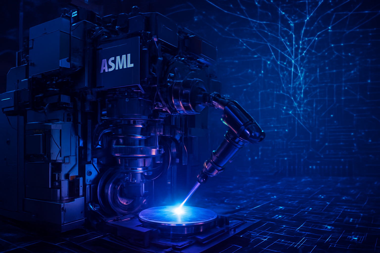
In a move that solidifies the next decade of semiconductor advancement, ASML (NASDAQ:ASML) has officially moved its High-NA (Numerical Aperture) EUV lithography systems from experimental pilots to commercial production. As of February 2, 2026, the Dutch lithography giant remains the world’s sole provider of these $400 million machines, a monopoly that effectively makes ASML the gatekeeper of the "Angstrom Era." This transition marks a pivotal moment for the industry, as leading-edge foundries race to operationalize the 1.4nm process node—a threshold essential for the next generation of generative AI and high-performance computing.
The immediate significance of this development cannot be overstated. With the shipment of the latest EXE:5200B systems to key partners, the semiconductor industry has officially entered a high-stakes transition period. While the previous generation of Low-NA EUV machines allowed the industry to reach the 3nm and 2nm milestones, the physical limits of light have necessitated this massive $400 million upgrade to keep Moore’s Law alive. The survival of the global AI roadmap now rests on ASML’s ability to scale production of these massive, complex tools.
The Technical Leap: Precision at the 8nm Limit
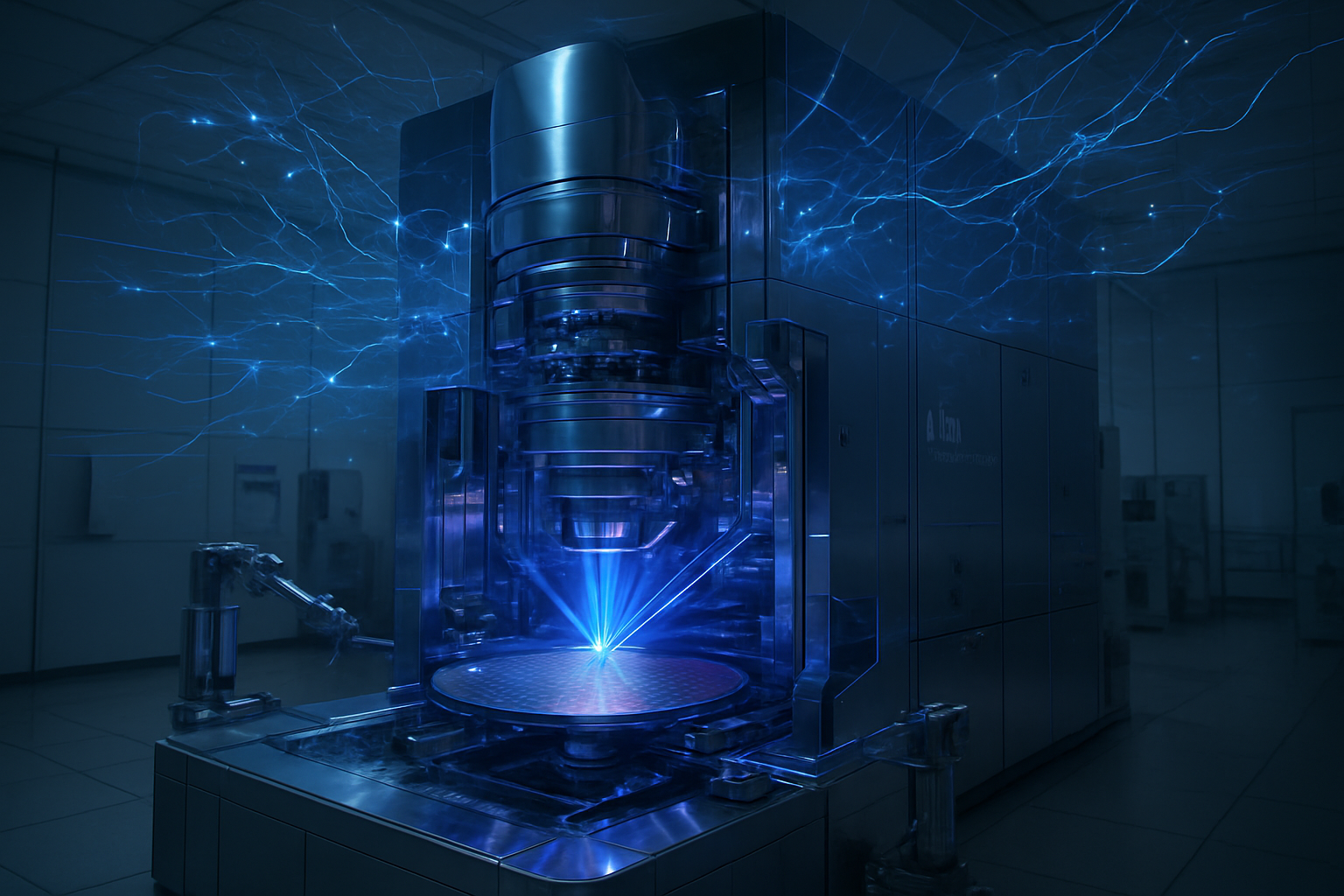
The technical core of this advancement lies in the increase of the Numerical Aperture from 0.33 in standard EUV machines to 0.55 in High-NA systems. This change allows for a significant improvement in resolution, dropping from approximately 13.5nm to a staggering 8nm. For manufacturers like Intel (NASDAQ:INTC), this enables the printing of ultra-fine transistor features in a single exposure. Previously, reaching these densities required "multi-patterning," a process where a single layer is printed multiple times to achieve the desired resolution—a method that is not only time-consuming but significantly increases the risk of defects and lower yields.
The new EXE:5200B systems represent a massive leap in throughput as well, capable of processing over 220 wafers per hour. This is a critical specification for high-volume manufacturing (HVM), as it offsets the astronomical cost of the equipment. Furthermore, the integration of High-NA lithography is coinciding with new transistor architectures like RibbonFET 2 (Intel’s second-generation Gate-All-Around) and advanced backside power delivery systems such as PowerDirect. These innovations, when combined with the precision of High-NA EUV, allow for a 15% to 20% improvement in performance-per-watt at the 1.4nm node.
Initial reactions from the semiconductor research community have been a mix of awe and caution. While experts at organizations like IMEC have lauded the successful realization of 8nm resolution, there is ongoing debate regarding the complexity of the new anamorphic lenses used in these machines. Unlike standard lenses, these optics provide different magnifications in the X and Y directions, requiring chip designers to rethink entire layout strategies. Despite these hurdles, the industry consensus is clear: High-NA is the only viable path to the 1.4nm (Intel 14A) and 1nm (Intel 10A) nodes.
A Fractured Competitive Landscape
The adoption of High-NA EUV has created a fascinating strategic divide among the world’s top chipmakers. Intel has taken a definitive first-mover advantage, being the first to receive and operationalize a fleet of High-NA tools at its Oregon D1X facility. CEO Pat Gelsinger’s "all-in" strategy is designed to reclaim process leadership from TSMC (NYSE:TSM) by 2026-2027. By mastering High-NA early, Intel aims to offer its 14A process to external foundry customers before its rivals, positioning itself as the premier manufacturer for the most advanced AI accelerators from companies like NVIDIA (NASDAQ:NVDA).
In contrast, TSMC has adopted a more conservative and cost-conscious approach. The world’s largest foundry is opting to push its existing 0.33 NA machines to their absolute limit, using complex multi-patterning for its initial A14 (1.4nm) node. TSMC’s leadership has publicly argued that High-NA remains too expensive for mass adoption in the immediate term, preferring to wait until the technology matures and costs normalize before integrating it into their high-volume lines for the A14P or A10 nodes. This creates a high-stakes gamble: can TSMC maintain its yield and cost advantages using older tools, or will Intel’s early adoption of High-NA allow it to leapfrog the industry leader in density and performance?
Meanwhile, Samsung (KRX:005930) is pursuing a hybrid strategy, utilizing its newly acquired High-NA systems for both its SF1.4 logic node and the development of next-generation Vertical Channel Transistor (VCT) DRAM. Samsung’s focus on AI-centric memory—specifically HBM4 and beyond—makes High-NA essential for maintaining its competitive edge in the memory market. This strategic divergence means that for the first time in a decade, the three major players are taking vastly different technological paths to reach the same destination, with ASML profiting from every choice made.
Moore’s Law in the Age of Artificial Intelligence
The broader significance of the High-NA era lies in its role as the physical foundation for the AI revolution. As Large Language Models (LLMs) grow in complexity, the demand for chips with higher transistor density and lower power consumption has become insatiable. The 1.4nm node is not just a numerical milestone; it represents the point where hardware can realistically support the trillion-parameter models expected by the end of the decade. Without the resolution provided by High-NA EUV, the energy requirements for training and inferencing these models would quickly become unsustainable for global power grids.
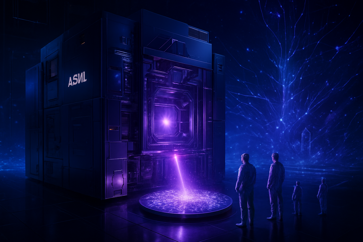
This development also underscores the extreme consolidation of the semiconductor supply chain. ASML’s €38.8 billion ($42.1B) order backlog represents a geopolitical reality where the entire world’s technological progress is bottlenecked through a single Dutch company. The concentration of such vital technology has already led to intense export controls and international friction. As we move toward 1.4nm, the "lithography gap" between those who have access to High-NA tools and those who do not will define the next era of economic and military power.
Comparatively, the shift to High-NA is being viewed as a milestone even more significant than the original transition from DUV (Deep Ultraviolet) to EUV in 2019. While that transition took nearly a decade of delays and false starts, the High-NA rollout has been remarkably precise, driven by the intense pressure of the AI "super-cycle." The success of this transition suggests that Moore's Law—frequently pronounced dead by skeptics—has found a new lease on life through sheer engineering willpower and massive capital investment.
The Horizon: From 1.4nm to the 1nm Threshold
Looking ahead, the next 24 to 36 months will be focused on the ramp-up to risk production for the 1.4nm node, expected in 2027. Near-term challenges remain, particularly regarding the development of new photoresists and mask-making materials that can keep up with the 8nm resolution of High-NA systems. Furthermore, the massive power consumption of these machines—each requiring its own dedicated electrical substation—will push semiconductor fabs to invest heavily in sustainable energy infrastructure.
Beyond 1.4nm lies the elusive 1nm (10 Angstrom) barrier. Experts predict that the EXE:5200 series will be the workhorse for this transition, but even higher NA systems or "Hyper-NA" (0.75 NA) are already being discussed in ASML’s R&D labs. Potential applications on the horizon include edge-AI chips so efficient they can run complex reasoning models on a smartphone battery for days, and specialized processors for quantum-classical hybrid systems. The primary hurdle will not just be physics, but economics: as tools approach the half-billion-dollar mark, only the largest sovereign-backed foundries may be able to afford to stay in the race.
Summary of the Angstrom Era
The successful commercialization of High-NA EUV by ASML marks a definitive end to the "nanometer" era and the beginning of the "Angstrom" era. By doubling down on its monopoly and delivering machines capable of 8nm resolution, ASML has provided a roadmap for Intel, Samsung, and TSMC to reach the 1.4nm node and beyond. Intel’s aggressive first-mover strategy stands in stark contrast to TSMC’s cautious optimization, setting the stage for a dramatic shift in market dynamics as we approach 2027.
The long-term impact of this development will be felt in every sector touched by AI, from autonomous systems to drug discovery. The ability to pack more intelligence into every square millimeter of silicon is the primary engine of modern progress. In the coming months, the industry will be watching for the first yield reports from Intel’s 14A pilot lines and ASML’s ability to meet its ambitious delivery schedule. One thing is certain: the path to 1.4nm is now open, but the cost of entry has never been higher.
This content is intended for informational purposes only and represents analysis of current AI developments.
TokenRing AI delivers enterprise-grade solutions for multi-agent AI workflow orchestration, AI-powered development tools, and seamless remote collaboration platforms.
For more information, visit https://www.tokenring.ai/.