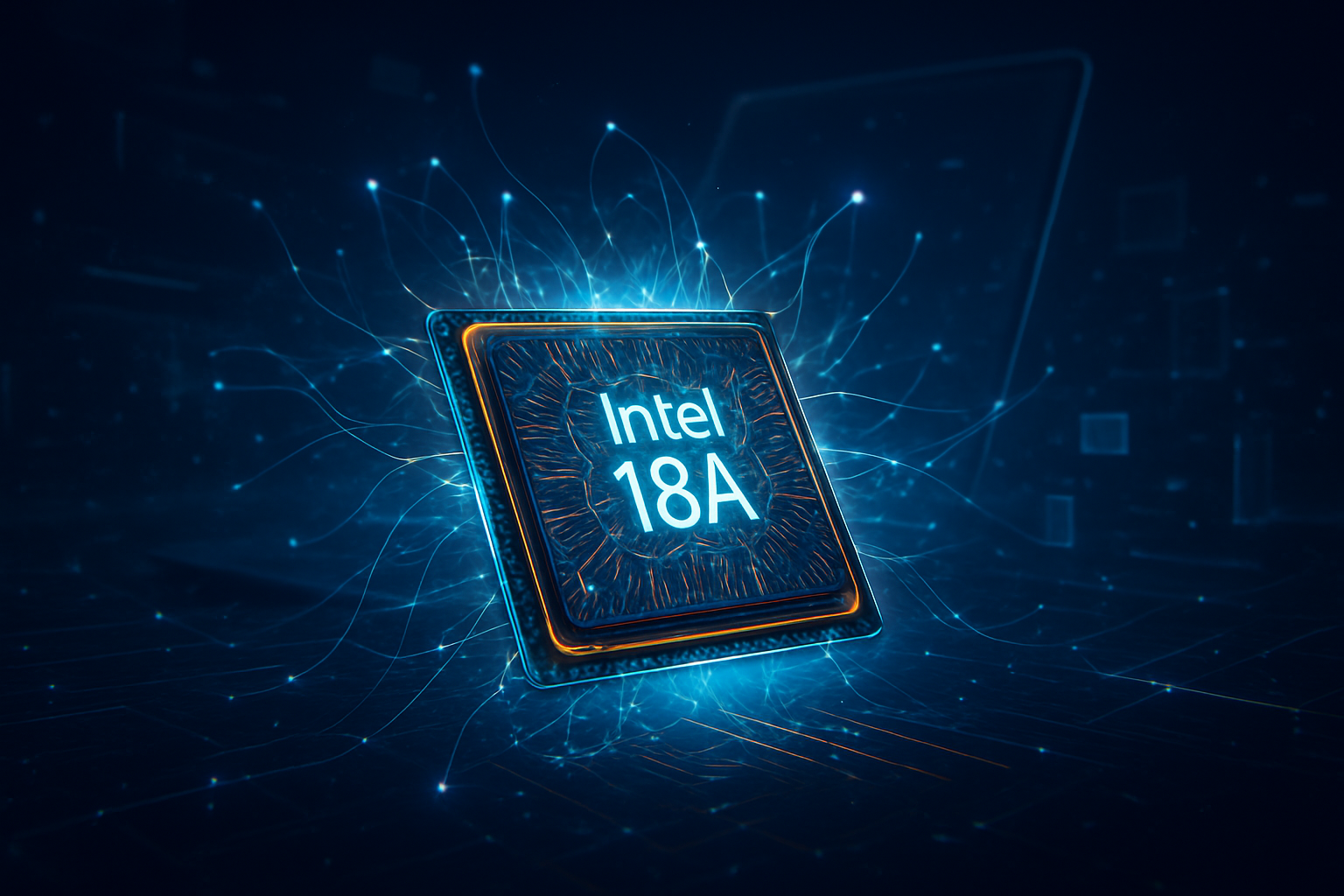
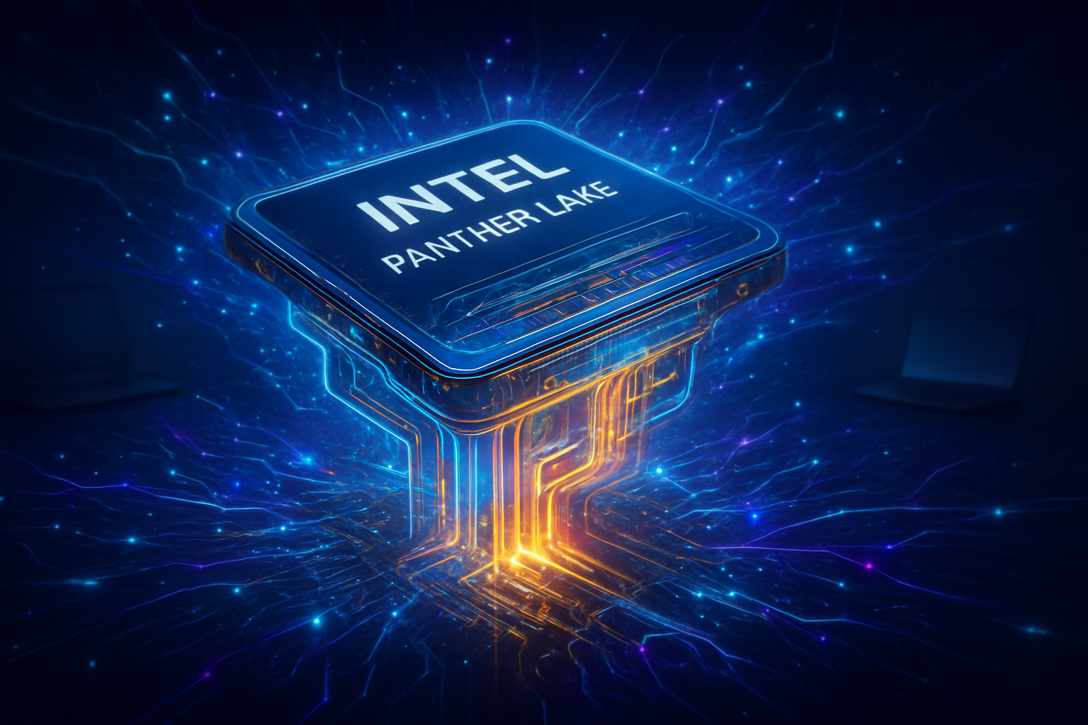
Tag: 18A Node

  • Intel’s Angstrom Era Arrives: How the 18A Node is Redefining the AI Silicon Landscape

    Intel’s Angstrom Era Arrives: How the 18A Node is Redefining the AI Silicon Landscape

    As of January 1, 2026, the global semiconductor landscape has undergone its most significant shift in over a decade. Intel Corporation (NASDAQ: INTC) has officially entered high-volume manufacturing (HVM) for its 18A (1.8nm) process node, marking the dawn of the "Angstrom Era." This milestone represents the successful completion of CEO Pat Gelsinger’s ambitious "five nodes in four years" strategy, a roadmap once viewed with skepticism by industry analysts but now realized as the foundation of Intel’s manufacturing resurgence.

    The 18A node is not merely a generational shrink in transistor size; it is a fundamental architectural pivot that introduces two "world-first" technologies to mass production: RibbonFET and PowerVia. By reaching this stage ahead of its primary competitors in key architectural metrics, Intel has positioned itself as a formidable "System Foundry," aiming to decouple its manufacturing prowess from its internal product design and challenge the long-standing dominance of Taiwan Semiconductor Manufacturing Company (NYSE: TSM).

    The Technical Backbone: RibbonFET and PowerVia

    The transition to the 18A node marks the end of the FinFET (Fin Field-Effect Transistor) era that has governed chip design since 2011. At the heart of 18A is RibbonFET, Intel’s implementation of a Gate-All-Around (GAA) transistor. Unlike FinFETs, where the gate covers the channel on three sides, RibbonFET surrounds the channel entirely with the gate. This configuration provides superior electrostatic control, drastically reducing power leakage—a critical requirement as transistors shrink toward atomic scales. Intel reports a 15% improvement in performance-per-watt over its previous Intel 3 node, allowing for more compute-intensive tasks without a proportional increase in thermal output.

    Even more significant is the debut of PowerVia, Intel’s proprietary backside power delivery technology. Historically, chips have been manufactured like a layered cake where both signal wires and power delivery lines are crowded onto the top "front" layers. PowerVia moves the power delivery to the backside of the wafer, decoupling it from the signal routing. This "world-first" implementation reduces voltage droop to less than 1%, down from the 6–7% seen in traditional designs, and improves cell utilization by up to 10%. By clearing the congestion on the front of the chip, Intel can drive higher clock speeds and achieve better thermal management, a massive advantage for the power-hungry processors required for modern AI workloads.

    Initial reactions from the semiconductor research community have been cautiously optimistic. While TSMC’s N2 (2nm) node, also ramping in early 2026, maintains a slight lead in raw transistor density, Intel’s 12-to-18-month head start in backside power delivery is seen as a strategic masterstroke. Experts note that for AI accelerators and high-performance computing (HPC) chips, the efficiency gains from PowerVia may outweigh the density advantages of competitors, making 18A the preferred choice for the next generation of data center silicon.

    A New Power Dynamic for AI Giants and Startups

    The success of 18A has immediate and profound implications for the world’s largest technology companies. Microsoft (NASDAQ: MSFT) has emerged as the lead external customer for Intel Foundry, utilizing the 18A node for its custom "Maia 2" and "Braga" AI accelerators. By partnering with Intel, Microsoft reduces its reliance on third-party silicon providers and gains access to a domestic supply chain, a move that significantly strengthens its competitive position against Google (NASDAQ: GOOGL) and Meta (NASDAQ: META).

    Amazon (NASDAQ: AMZN) has also committed to the 18A node for its AWS Trainium3 chips and custom AI networking fabric. For Amazon, the efficiency gains of PowerVia translate directly into lower operational costs for its massive data center footprint. Meanwhile, the broader Arm (NASDAQ: ARM) ecosystem is gaining a foothold on Intel’s manufacturing lines through partnerships with Faraday Technology, signaling that Intel is finally serious about becoming a neutral "System Foundry" capable of producing chips for any architecture, not just x86.

    This development creates a high-stakes competitive environment for NVIDIA (NASDAQ: NVDA). While NVIDIA has traditionally relied on TSMC for its cutting-edge GPUs, the arrival of a viable 18A node provides NVIDIA with critical leverage in price negotiations and a potential "Plan B" for domestic manufacturing. The market positioning of Intel Foundry as a "Western-based alternative" to TSMC is already disrupting the strategic roadmaps of startups and established giants alike, as they weigh the benefits of Intel’s new architecture against the proven scale of the Taiwanese giant.

    Geopolitics and the Broader AI Landscape

    The launch of 18A is more than a corporate victory; it is a cornerstone of the broader effort to re-shore advanced semiconductor manufacturing to the United States. Supported by the CHIPS and Science Act, Intel’s Fab 52 in Arizona is now the most advanced logic manufacturing facility in the Western Hemisphere. In an era where AI compute is increasingly viewed as a matter of national security, the ability to produce 1.8nm chips domestically provides a buffer against potential supply chain disruptions in the Taiwan Strait.

    Within the AI landscape, the "Angstrom Era" addresses the most pressing bottleneck: the energy crisis of the data center. As Large Language Models (LLMs) continue to scale, the power required to train and run them has become a limiting factor. The 18A node’s focus on performance-per-watt is a direct response to this trend. By enabling more efficient AI accelerators, Intel is helping to sustain the current pace of AI breakthroughs, which might otherwise have been slowed by the physical limits of power and cooling.

    However, concerns remain regarding Intel’s ability to maintain high yields. As of early 2026, reports suggest 18A yields are hovering between 60% and 65%. While sufficient for commercial production, this is lower than the 75%+ threshold typically associated with high-margin profitability. The industry is watching closely to see if Intel can refine the process quickly enough to satisfy the massive volume demands of customers like Microsoft and the U.S. Department of Defense.

    The Road to 14A and Beyond

    Looking ahead, the 18A node is just the beginning of the Angstrom Era. Intel has already begun the installation of High-NA (Numerical Aperture) EUV lithography machines—the most expensive and complex tools in human history—to prepare for the Intel 14A (1.4nm) node. Slated for risk production in 2027, 14A is expected to provide another 15% leap in performance, further cementing Intel’s goal of undisputed process leadership by the end of the decade.

    The immediate next steps involve the retail rollout of Panther Lake (Core Ultra Series 3) and the data center launch of Clearwater Forest (Xeon). These internal products will serve as the "canaries in the coal mine" for the 18A process. If these chips deliver the promised performance gains in real-world consumer and enterprise environments over the next six months, it will likely trigger a wave of new foundry customers who have been waiting for proof of Intel’s manufacturing stability.

    Experts predict that the next two years will see an "architecture war" where the physical design of the transistor (GAA vs. FinFET) and the method of power delivery (Backside vs. Frontside) become as important as the nanometer label itself. As TSMC prepares its own backside power solution (A16) for late 2026, Intel’s ability to capitalize on its current lead will determine whether it can truly reclaim the crown it lost a decade ago.

    Summary of the Angstrom Era Transition

    The arrival of Intel 18A marks a historic turning point in the semiconductor industry. By successfully delivering RibbonFET and PowerVia, Intel has not only met its technical goals but has also fundamentally changed the competitive dynamics of the AI era. The node provides a crucial domestic alternative for AI giants like Microsoft and Amazon, while offering a technological edge in power efficiency that is essential for the next generation of high-performance computing.

    The significance of this development in AI history cannot be overstated. We are moving from a period of "AI at any cost" to an era of "sustainable AI compute," where the efficiency of the underlying silicon is the primary driver of innovation. Intel’s 18A node is the first major step into this new reality, proving that Moore's Law—though increasingly difficult to maintain—is still alive and well in the Angstrom Era.

    In the coming months, the industry should watch for yield improvements at Fab 52 and the first independent benchmarks of Panther Lake. These metrics will be the ultimate judge of whether Intel’s "5 nodes in 4 years" was a successful gamble or a temporary surge. For now, the "Angstrom Era" has officially begun, and the world of AI silicon will never be the same.


    This content is intended for informational purposes only and represents analysis of current AI developments.

    TokenRing AI delivers enterprise-grade solutions for multi-agent AI workflow orchestration, AI-powered development tools, and seamless remote collaboration platforms.
    For more information, visit https://www.tokenring.ai/.

  • Intel Seizes Manufacturing Crown: World’s First High-NA EUV Production Line Hits 30,000 Wafers per Quarter for 18A Node

    Intel Seizes Manufacturing Crown: World’s First High-NA EUV Production Line Hits 30,000 Wafers per Quarter for 18A Node

    In a move that signals a seismic shift in the global semiconductor landscape, Intel (NASDAQ: INTC) has officially transitioned its most advanced manufacturing process into high-volume production. By successfully processing 30,000 wafers per quarter using the world’s first High-NA (Numerical Aperture) Extreme Ultraviolet (EUV) lithography machines, the company has reached a critical milestone for its 18A (1.8nm) process node. This achievement represents the first time these $380 million machines, manufactured by ASML (NASDAQ: ASML), have been utilized at such a scale, positioning Intel as the current technological frontrunner in the race to sub-2nm chip manufacturing.

    The significance of this development cannot be overstated. For nearly a decade, Intel struggled to maintain its lead against rivals like TSMC (NYSE: TSM) and Samsung (KRX: 005930), but the aggressive adoption of High-NA EUV technology appears to be the "silver bullet" the company needed. By hitting the 30,000-wafer mark as of late 2025, Intel is not just testing prototypes; it is proving that the most complex manufacturing equipment ever devised by humanity is ready for the demands of the AI-driven global economy.

    Technical Breakthrough: The Power of 0.55 NA

    The technical backbone of this milestone is the ASML Twinscan EXE:5200, a machine that stands as a marvel of modern physics. Unlike standard EUV machines that utilize a 0.33 Numerical Aperture, High-NA EUV increases this to 0.55. This allows for a significantly finer focus of the EUV light, enabling the printing of features as small as 8nm in a single exposure. In previous generations, achieving such tiny dimensions required "multi-patterning," a process where a single layer of a chip is passed through the machine multiple times. Multi-patterning is notoriously expensive, time-consuming, and prone to alignment errors that can ruin an entire wafer of chips.

    By moving to single-exposure 8nm printing, Intel has effectively slashed the complexity of its manufacturing flow. Industry experts note that High-NA EUV can reduce the number of processing steps for critical layers by nearly 50%, which theoretically leads to higher yields and faster production cycles. Furthermore, the 18A node introduces two other foundational technologies: RibbonFET (Intel’s implementation of Gate-All-Around transistors) and PowerVia (a revolutionary backside power delivery system). While RibbonFET improves transistor performance, PowerVia solves the "wiring bottleneck" by moving power lines to the back of the silicon, leaving more room for data signals on the front.

    Initial reactions from the AI research community and semiconductor analysts have been cautiously optimistic. While TSMC has historically been more conservative, opting to stick with older Low-NA machines for its 2nm (N2) node to save costs, Intel’s "all-in" gamble on High-NA is being viewed as a high-risk, high-reward strategy. If Intel can maintain stable yields at 30,000 wafers per quarter, it will have a clear path to reclaiming the "process leadership" title it lost in the mid-2010s.

    Industry Disruption: A New Challenger for AI Silicon

    The implications for the broader tech industry are profound. For years, the world’s leading AI labs and hardware designers—including NVIDIA (NASDAQ: NVDA), Apple (NASDAQ: AAPL), and AMD (NASDAQ: AMD)—have been almost entirely dependent on TSMC for their most advanced silicon. Intel’s successful ramp-up of the 18A node provides a viable second source for high-performance AI chips, which could lead to more competitive pricing and a more resilient global supply chain.

    For Intel Foundry, this is a "make or break" moment. The company is positioning itself to become the world’s second-largest foundry by 2030, and the 18A node is its primary lure for external customers. Microsoft (NASDAQ: MSFT) has already signed on as a major customer for the 18A process, and other tech giants are reportedly monitoring Intel’s yield rates closely. If Intel can prove that High-NA EUV provides a cost-per-transistor advantage over TSMC’s multi-patterning approach, we could see a significant migration of chip designs toward Intel’s domestic Fabs in Arizona and Ohio.

    However, the competitive landscape remains fierce. While Intel leads in the adoption of High-NA, TSMC’s N2 node is expected to be extremely mature and high-yielding by 2026. The market positioning now comes down to a battle between Intel’s architectural innovation (High-NA + PowerVia) and TSMC’s legendary manufacturing consistency. For startups and smaller AI companies, Intel's emergence as a top-tier foundry could provide easier access to cutting-edge silicon that was previously reserved for the industry's largest players.

    Geopolitical and Scientific Significance

    Looking at the wider significance, the success of the 18A node is a testament to the continued survival of Moore’s Law. Many critics argued that as we approached the 1nm limit, the physical and financial hurdles would become insurmountable. Intel’s 30,000-wafer milestone proves that through massive capital investment and international collaboration—specifically between the US-based Intel and the Netherlands-based ASML—the industry can continue to scale.

    This development also carries heavy geopolitical weight. As the US government continues to push for domestic semiconductor self-sufficiency through the CHIPS Act, Intel’s Fab 52 in Arizona has become a symbol of American industrial resurgence. The ability to produce the world’s most advanced AI processors on US soil reduces reliance on East Asian supply chains, which are increasingly seen as a point of strategic vulnerability.

    Comparatively, this milestone mirrors the transition to EUV lithography nearly a decade ago. At that time, those who adopted EUV early (like TSMC) gained a massive advantage, while those who delayed (like Intel) fell behind. By being the first to cross the High-NA finish line, Intel is attempting to flip the script, forcing its competitors to play catch-up with a technology that costs nearly $400 million per machine and requires a complete overhaul of fab logistics.

    The Road to 1nm: What Lies Ahead

    Looking ahead, the near-term focus for Intel will be the full-scale launch of "Panther Lake" and "Clearwater Forest"—the first internal products to utilize the 18A node. These chips are expected to hit the market in early 2026, serving as the ultimate test of the 18A process in real-world AI PC and server environments. If these products perform as expected, the next step will be the 14A node, which is designed to be "High-NA native" from the ground up.

    The long-term roadmap involves scaling toward the 10A (1nm) node by the end of the decade. Challenges remain, particularly regarding the power consumption of these massive High-NA machines and the extreme precision required to maintain 0.7nm overlay accuracy. Experts predict that the next two years will be defined by a "yield war," where the winner is not just the company with the best machine, but the one that can most efficiently manage the data and chemistry required to keep those machines running 24/7.

    Conclusion: A New Era of Computing

    Intel’s achievement of processing 30,000 wafers per quarter on the 18A node marks a historic turning point. It validates the use of High-NA EUV as a viable production technology and sets the stage for a new era of AI hardware. By integrating 8nm single-exposure printing with RibbonFET and PowerVia, Intel has built a formidable technological stack that challenges the status quo of the semiconductor industry.

    As we move into 2026, the industry will be watching for two things: the real-world performance of Intel’s first 18A chips and the response from TSMC. If Intel can maintain its momentum, it will have successfully executed one of the most difficult corporate turnarounds in tech history. For now, the "blue team" has reclaimed the technical high ground, and the future of AI silicon looks more competitive than ever.


    This content is intended for informational purposes only and represents analysis of current AI developments.

    TokenRing AI delivers enterprise-grade solutions for multi-agent AI workflow orchestration, AI-powered development tools, and seamless remote collaboration platforms.
    For more information, visit https://www.tokenring.ai/.

  • Intel Closes in on Historic Deal to Manufacture Apple M-Series Chips on 18A Node by 2027

    Intel Closes in on Historic Deal to Manufacture Apple M-Series Chips on 18A Node by 2027

    In what is being hailed as a watershed moment for the global semiconductor industry, Apple Inc. (NASDAQ: AAPL) has reportedly begun the formal qualification process for Intel’s (NASDAQ: INTC) 18A manufacturing node. According to industry insiders and supply chain reports surfacing in late 2025, the two tech giants are nearing a definitive agreement that would see Intel manufacture entry-level M-series silicon for future MacBooks and iPads starting in 2027. This potential partnership marks the first time Intel would produce chips for Apple since the Cupertino-based company famously transitioned to its own ARM-based "Apple Silicon" and severed its processor supply relationship with Intel in 2020.

    The significance of this development cannot be overstated. For Apple, the move represents a strategic pivot toward geopolitical "de-risking," as the company seeks to diversify its advanced-node supply chain away from its near-total reliance on Taiwan Semiconductor Manufacturing Company (NYSE: TSM). For Intel, securing Apple as a foundry customer would serve as the ultimate validation of its "five nodes in four years" roadmap and its ambitious transformation into a world-class contract manufacturer. If the deal proceeds, it would signal a profound "manufacturing renaissance" for the United States, bringing the production of the world’s most advanced consumer electronics back to American soil.

    The Technical Leap: RibbonFET, PowerVia, and the 18AP Variant

    The technical foundation of this deal rests on Intel’s 18A (1.8nm-class) process, which is widely considered the company’s "make-or-break" node. Unlike previous generations, 18A introduces two revolutionary architectural shifts: RibbonFET and PowerVia. RibbonFET is Intel’s implementation of Gate-All-Around (GAA) transistor technology, which replaces the long-standing FinFET design. By surrounding the transistor channel with the gate on all four sides, RibbonFET significantly reduces power leakage and allows for higher drive currents at lower voltages. This is paired with PowerVia, a breakthrough "backside power delivery" system that moves power routing to the reverse side of the wafer. By separating the power and signal lines, Intel has managed to reduce voltage drop to less than 1%, compared to the 6–7% seen in traditional front-side delivery systems, while simultaneously improving chip density.

    According to leaked documents from November 2025, Apple has already received version 0.9.1 GA of the Intel 18AP Process Design Kit (PDK). The "P" in 18AP stands for "Performance," a specialized variant of the 18A node optimized for high-efficiency consumer devices. Reports suggest that 18AP offers a 15% to 20% improvement in performance-per-watt over the standard 18A node, making it an ideal candidate for Apple’s high-volume, entry-level chips like the upcoming M6 or M7 base models. Apple’s engineering teams are currently engaged in intensive architectural modeling to ensure that Intel’s yields can meet the rigorous quality standards that have historically made TSMC the gold standard of the industry.

    The reaction from the AI research and semiconductor communities has been one of cautious optimism. While TSMC remains the leader in volume and reliability, analysts note that Intel’s early lead in backside power delivery gives them a unique competitive edge. Experts suggest that if Intel can successfully scale 18A production at its Fab 52 facility in Arizona, it could match or even exceed the power efficiency of TSMC’s 2nm (N2) node, which Apple is currently using for its flagship "Pro" and "Max" chips.

    Shifting the Competitive Landscape for Tech Giants

    The potential deal creates a new "dual-foundry" reality that fundamentally alters the power dynamics between the world’s largest tech companies. For years, Apple has been TSMC’s most important customer, often receiving exclusive first-access to new nodes. By bringing Intel into the fold, Apple gains immense bargaining power and a critical safety net. This strategy allows Apple to bifurcate its lineup: keeping its highest-end "Pro" and "Max" chips with TSMC in Taiwan and Arizona, while shifting its massive volume of entry-level MacBook Air and iPad silicon to Intel’s domestic fabs.

    This development also has major implications for other industry leaders like Nvidia (NASDAQ: NVDA) and Microsoft (NASDAQ: MSFT). Both companies have already expressed interest in Intel Foundry, but an "Apple-certified" 18A process would likely trigger a stampede of other fabless chip designers toward Intel. If Intel can prove it can handle the volume and complexity of Apple's designs, it effectively removes the "reputational risk" that has hindered Intel Foundry’s growth in its early years. Conversely, for TSMC, the loss of even a portion of Apple’s business represents a significant long-term threat to its market dominance, forcing the Taiwanese firm to accelerate its own US-based expansion and innovate even faster to maintain its lead.

    Furthermore, the split of Intel’s manufacturing business into a separate subsidiary—Intel Foundry—has been a masterstroke in building trust. By maintaining a separate profit-and-loss (P&L) statement and strict data firewalls, Intel has convinced Apple that its proprietary chip designs will remain secure from Intel’s own product divisions. This structural change was a prerequisite for Apple even considering a return to the Intel ecosystem.

    Geopolitics and the Quest for Semiconductor Sovereignty

    Beyond the technical and commercial aspects, the Apple-Intel deal is deeply rooted in the broader geopolitical struggle for semiconductor sovereignty. In the current climate of late 2025, "concentration risk" in the Taiwan Strait has become a primary concern for the US government and Silicon Valley executives alike. Apple’s move is a direct response to this instability, aligning with CEO Tim Cook’s 2025 pledge to invest heavily in a domestic silicon supply chain. By utilizing Intel’s facilities in Oregon and Arizona, Apple is effectively "onshoring" the production of its most popular products, insulating itself from potential trade disruptions or regional conflicts.

    This shift also highlights the success of the US CHIPS and Science Act, which provided the financial framework for Intel’s massive fab expansions. In late 2025, the US government finalized an $8.9 billion equity investment in Intel, effectively cementing the company’s status as a "National Strategic Asset." This government backing ensures that Intel has the capital necessary to compete with the subsidized giants of East Asia. For the first time in decades, the United States is positioned to host the manufacturing of sub-2nm logic chips, a feat that seemed impossible just five years ago.

    However, this "manufacturing renaissance" is not without its critics. Some industry analysts worry that the heavy involvement of the US government could lead to inefficiencies or that Intel may struggle to maintain the relentless pace of innovation required to stay at the leading edge. Comparisons are often made to the early days of the semiconductor industry, but the scale of today’s technology is vastly more complex. The success of the 18A node is not just a corporate milestone for Intel; it is a test case for whether Western nations can successfully reclaim the heights of advanced manufacturing.

    The Road to 2027 and the 14A Horizon

    Looking ahead, the next 12 to 18 months will be critical. Apple is expected to make a final "go/no-go" decision by the first quarter of 2026, following the release of Intel’s finalized 1.0 PDK. If the qualification is successful, Intel will begin the multi-year process of "ramping" the 18A node for mass production. This involves fine-tuning the High-NA EUV (Extreme Ultraviolet) lithography machines that Intel has been pioneered in its Oregon research facilities. These $380 million machines from ASML are the key to reaching even smaller dimensions, and Intel's early adoption of this technology is a major factor in Apple's interest.

    The roadmap doesn't stop at 18A. Reports indicate that Apple is already looking toward Intel’s 14A (1.4nm) process for 2028 and beyond. This suggests that the 2027 deal is not a one-off experiment but the beginning of a long-term strategic partnership. As AI applications continue to demand more compute power and better energy efficiency, the ability to manufacture at the 1.4nm level will be the next great frontier. We can expect to see future M-series chips leveraging these nodes to integrate even more advanced neural engines and on-device AI capabilities that were previously relegated to the cloud.

    The challenges remain significant. Intel must prove it can achieve the high yields necessary for Apple’s massive product launches, which often require tens of millions of chips in a single quarter. Any delays in the 18A ramp could have a domino effect on Apple’s product release cycles. Experts predict that the first half of 2026 will be defined by "yield-watch" reports as the industry monitors Intel's progress in translating laboratory success into factory floor reality.

    A New Era for Silicon Valley

    The potential return of Apple to Intel’s manufacturing plants marks the end of one era and the beginning of another. It signifies a move away from the "fabless" versus "integrated" dichotomy of the past decade and toward a more collaborative, geographically diverse ecosystem. If the 2027 production timeline holds, it will be remembered as the moment the US semiconductor industry regained its footing on the global stage, proving that it could still compete at the absolute bleeding edge of technology.

    For the consumer, this deal promises more efficient, more powerful devices that are less susceptible to global supply chain shocks. For the industry, it provides a much-needed second source for advanced logic, breaking the effective monopoly that TSMC has held over the high-end market. As we move into 2026, all eyes will be on the test wafers coming out of Intel’s Arizona fabs. The stakes could not be higher: the future of the Mac, the viability of Intel Foundry, and the technological sovereignty of the United States all hang in the balance.


    This content is intended for informational purposes only and represents analysis of current AI and semiconductor developments.

    TokenRing AI delivers enterprise-grade solutions for multi-agent AI workflow orchestration, AI-powered development tools, and seamless remote collaboration platforms.
    For more information, visit https://www.tokenring.ai/.

  • Intel’s 18A Node Hits Volume Production at Fab 52 as Yields Stabilize for Panther Lake Ramp

    Intel’s 18A Node Hits Volume Production at Fab 52 as Yields Stabilize for Panther Lake Ramp

    Intel Corporation (NASDAQ:INTC) has officially reached a historic milestone in the semiconductor race, announcing that its 18A (1.8nm-class) process node has entered high-volume manufacturing (HVM) at the newly operational Fab 52 in Arizona. This achievement marks the successful completion of CEO Pat Gelsinger’s ambitious "five nodes in four years" roadmap, positioning the American chipmaker as the first in the world to deploy 2nm-class technology at scale. As of late December 2025, the 18A node is powering the initial production ramp of the "Panther Lake" processor family, a critical product designed to cement Intel’s leadership in the burgeoning AI PC market.

    The transition to volume production at the $30 billion Fab 52 facility is a watershed moment for the U.S. semiconductor industry. While the journey to 18A was marked by skepticism from Wall Street and technical hurdles, internal reports now indicate that manufacturing yields have stabilized significantly. After trailing the mature yields of Taiwan Semiconductor Manufacturing Co. (NYSE:TSM) earlier in the year, Intel’s 18A process has shown a steady improvement of approximately 7% per month. Yields reached the 60-65% range in November, and the company is currently on track to hit its 70% target by the close of 2025, providing the necessary economic foundation for both internal products and external foundry customers.

    The Architecture of Leadership: RibbonFET and PowerVia

    The 18A node represents more than just a shrink in transistor size; it introduces the most significant architectural shifts in semiconductor manufacturing in over a decade. At the heart of 18A are two foundational technologies: RibbonFET and PowerVia. RibbonFET is Intel’s implementation of Gate-All-Around (GAA) transistors, which replaces the long-standing FinFET design. By wrapping the gate around all four sides of the transistor channel, RibbonFET provides superior electrostatic control, drastically reducing power leakage and allowing for higher drive currents. This results in a reported 25% performance-per-watt improvement over previous generations, a vital metric for AI-heavy workloads that demand extreme efficiency.

    Complementing RibbonFET is PowerVia, Intel’s industry-first commercialization of backside power delivery. Traditionally, power and signal lines are bundled together on the front of a chip, leading to "voltage droop" and routing congestion. PowerVia moves the power delivery network to the back of the silicon wafer, separating it from the signal lines. This decoupling allows for a 10% reduction in IR (voltage) droop and frees up significant space for signal routing, enabling a 0.72x area reduction compared to the Intel 3 node. This dual-innovation approach has allowed Intel to leapfrog competitors who are not expected to integrate backside power until their 2nm or sub-2nm nodes in 2026.

    Industry experts have noted that the stabilization of 18A yields is a testament to Intel’s aggressive use of ASML (NASDAQ:ASML) Twinscan NXE:3800E Low-NA EUV lithography systems. While the industry initially questioned Intel’s decision to skip High-NA EUV for the 18A node in favor of refined Low-NA techniques, the current volume ramp suggests the gamble has paid off. By perfecting the manufacturing process on existing equipment, Intel has managed to reach HVM ahead of TSMC’s N2 (2nm) schedule, which is not expected to see similar volume until mid-to-late 2026.

    Shifting the Competitive Landscape: Intel Foundry vs. The World

    The successful ramp of 18A at Fab 52 has immediate and profound implications for the global foundry market. For years, TSMC has held a near-monopoly on leading-edge manufacturing, serving giants like Apple (NASDAQ:AAPL) and NVIDIA (NASDAQ:NVDA). However, Intel’s progress is already drawing significant interest from "anchor" foundry customers. Microsoft (NASDAQ:MSFT) and Amazon (NASDAQ:AMZN) have already committed to using the 18A node for their custom AI silicon, seeking to diversify their supply chains and reduce their total reliance on Taiwanese fabrication.

    The competitive pressure is now squarely on Samsung (KRX:005930) and TSMC. While Samsung was the first to introduce GAA at 3nm, it struggled with yield issues that prevented widespread adoption. Intel’s ability to hit 60-65% yields on a more advanced 1.8nm-class node puts it in a prime position to capture market share from customers who are wary of Samsung’s consistency. For TSMC, the threat is more strategic; Intel is no longer just a designer of CPUs but a direct competitor in the high-margin foundry business. If Intel can maintain its 7% monthly yield improvement trajectory, it may offer a cost-competitive alternative to TSMC’s upcoming N2 node by the time the latter reaches volume.

    Furthermore, the "Panther Lake" ramp serves as a crucial internal proof of concept. By manufacturing 70% of the Panther Lake die area in-house on 18A, Intel is reducing its multi-billion dollar payments to external foundries. This vertical integration—the "IDM 2.0" strategy—is designed to improve Intel’s gross margins, which have been under pressure during this intensive capital expenditure phase. If Panther Lake meets its performance targets in the retail market this month, it will signal to the entire industry that Intel’s manufacturing engine is once again firing on all cylinders.

    Geopolitics and the AI Infrastructure Era

    The broader significance of 18A production at Fab 52 cannot be overstated in the context of global technopolitics. As the U.S. government seeks to "re-shore" critical technology through the CHIPS and Science Act, Intel’s Arizona facility stands as the premier example of domestic leading-edge manufacturing. The 18A node is already the designated process for the Department of Defense’s "Secure Enclave" program, ensuring that the next generation of American defense and intelligence hardware is built on home soil. This creates a "moat" for Intel that is as much about national security as it is about transistor density.

    In the AI landscape, the 18A node arrives at a pivotal moment. The current "AI PC" trend requires processors that can handle complex neural network tasks locally without sacrificing battery life. The efficiency gains from RibbonFET and PowerVia are specifically tailored for these use cases. By being the first to reach 2nm-class production, Intel is providing the hardware foundation for the next wave of generative AI applications, potentially shifting the balance of power in the laptop and workstation markets back in its favor after years of gains by ARM-based (NASDAQ:ARM) competitors.

    This milestone also marks the end of an era of uncertainty for Intel. The "five nodes in four years" promise was often viewed as a marketing slogan rather than a realistic engineering goal. By delivering 18A in volume by the end of 2025, Intel has restored its credibility with investors and partners alike. This achievement echoes the "Tick-Tock" era of Intel’s past dominance, suggesting that the company has finally overcome the 10nm and 7nm delays that plagued it for nearly a decade.

    The Road to 14A and High-NA EUV

    Looking ahead, the success of 18A is the springboard for Intel’s next ambitious phase: the 14A (1.4nm) node. While 18A utilized refined Low-NA EUV, the 14A node will be the first to implement ASML’s High-NA EUV lithography at scale. Intel has already taken delivery of the first High-NA machines at its Oregon R&D site, and the lessons learned from the 18A ramp at Fab 52 will be instrumental in perfecting the next generation of patterning.

    In the near term, the industry will be watching the ramp of "Clearwater Forest," the 18A-based Xeon processor scheduled for early 2026. While Panther Lake addresses the consumer market, Clearwater Forest will be the true test of 18A’s viability in the high-stakes data center market. If Intel can deliver superior performance-per-watt in the server space, it could halt the market share erosion it has faced at the hands of AMD (NASDAQ:AMD).

    Challenges remain, particularly in scaling the 18A process to meet the diverse needs of dozens of foundry customers, each with unique design rules. However, the current trajectory suggests that Intel is well-positioned to reclaim the "manufacturing crown" by 2026. Analysts predict that if yields hit the 70% target by early 2026, Intel Foundry could become a profitable standalone entity sooner than originally anticipated, fundamentally altering the economics of the semiconductor industry.

    A New Chapter for Silicon

    The commencement of volume production at Fab 52 is more than just a corporate achievement; it is a signal that the semiconductor industry remains a field of rapid, disruptive innovation. Intel’s 18A node combines the most advanced transistor architecture with a revolutionary power delivery system, setting a new benchmark for what is possible in silicon. As Panther Lake chips begin to reach consumers this month, the world will get its first taste of the 1.8nm era.

    The key takeaways from this development are clear: Intel has successfully navigated its most difficult technical transition in history, the U.S. has regained a foothold in leading-edge manufacturing, and the race for AI hardware supremacy has entered a new, more competitive phase. The next few months will be critical as Intel moves from "stabilizing" yields to "optimizing" them for a global roster of clients.

    For the tech industry, the message is undeniable: the "Intel is back" narrative is no longer just a projection—it is being etched into silicon in the Arizona desert. As 2025 draws to a close, the focus shifts from whether Intel can build the future to how fast they can scale it.


    This content is intended for informational purposes only and represents analysis of current AI and semiconductor developments.

    TokenRing AI delivers enterprise-grade solutions for multi-agent AI workflow orchestration, AI-powered development tools, and seamless remote collaboration platforms.
    For more information, visit https://www.tokenring.ai/.