Tag: 18A

  • The Silicon Renaissance: Intel Arizona Hits High-Volume Production in CHIPS Act Victory

    The Silicon Renaissance: Intel Arizona Hits High-Volume Production in CHIPS Act Victory

    In a landmark moment for the American semiconductor industry, Intel Corporation (NASDAQ:INTC) has officially commenced high-volume manufacturing (HVM) of its cutting-edge 18A (1.8nm-class) process technology at its Fab 52 facility in Ocotillo, Arizona. This achievement marks the first time a United States-based fabrication plant has successfully surpassed the 2nm threshold, effectively reclaiming a technological lead that had shifted toward East Asia over the last decade. The milestone is being hailed as the "Silicon Renaissance," signaling that the aggressive "five nodes in four years" roadmap championed by Intel leadership has reached its most critical objective.

    The start of production at Fab 52 serves as a definitive victory for the U.S. CHIPS and Science Act, providing tangible evidence that multi-billion dollar federal investments are translating into domestic manufacturing capacity for the world’s most advanced logic chips. While the broader domestic expansion has faced hurdles—most notably the "Silicon Heartland" project in New Albany, Ohio, which saw its first fab delayed until 2030—the Arizona breakthrough provides a vital anchor for the domestic supply chain. By securing high-volume production of 1.8nm chips on American soil, the move significantly bolsters national security and reduces the industry's reliance on sensitive geopolitical regions for high-end AI and defense silicon.

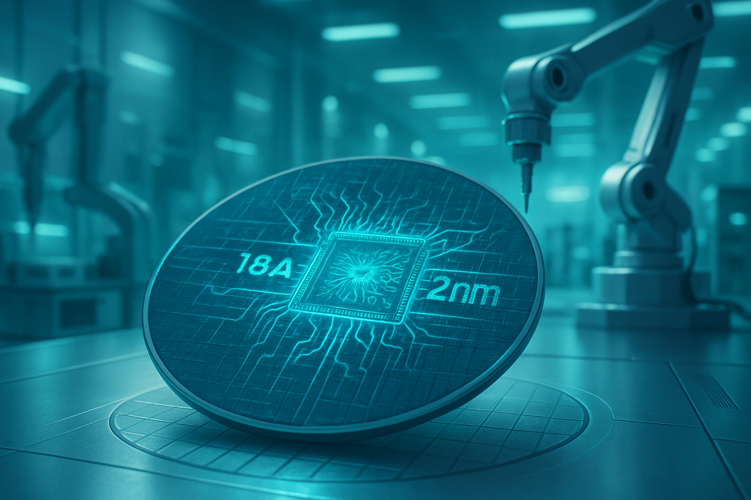
    The Intel 18A process is not merely a refinement of existing technology; it represents a fundamental architectural shift in how semiconductors are built. At the heart of this transition are two revolutionary technologies: RibbonFET and PowerVia. RibbonFET is Intel’s implementation of a Gate-All-Around (GAA) transistor architecture, which replaces the FinFET design that has dominated the industry for over a decade. By surrounding the conducting channel on all four sides with the gate, RibbonFET allows for superior electrostatic control, drastically reducing power leakage and enabling faster switching speeds at lower voltages. This is paired with PowerVia, a pioneering "backside power delivery" system that separates power routing from signal lines by moving it to the reverse side of the wafer.

    Technical specifications for the 18A node are formidable. Compared to previous generations, 18A offers a 30% improvement in logic density and can deliver up to 38% lower power consumption at equivalent performance levels. Initial data from Fab 52 indicates that the implementation of PowerVia has reduced "IR droop" (voltage drop) by approximately 10%, leading to a 6% to 10% frequency gain in early production units. This technical leap puts Intel ahead of its primary rival, Taiwan Semiconductor Manufacturing Company (NYSE:TSM), in the specific implementation of backside power delivery, a feature TSMC is not expected to deploy in high volume until its N2P or A16 nodes later this year or in 2027.

    The AI research community and industry experts have reacted with cautious optimism. While the technical achievement of 18A is undeniable, the focus has shifted toward yield rates. Internal reports suggest that Fab 52 is currently seeing yields in the 55–65% range—a respectable start for a sub-2nm node but still below the 75-80% "industry standard" typically required for high-margin external foundry services. Nevertheless, the successful integration of these technologies into high-volume manufacturing confirms that Intel’s engineering teams have solved the primary physics challenges associated with Angstrom-era lithography.

    The implications for the broader tech ecosystem are profound, particularly for the burgeoning AI sector. Intel Foundry Services (IFS) is now positioned as a viable alternative for tech giants looking to diversify their manufacturing partners. Microsoft Corporation (NASDAQ:MSFT) and Amazon.com, Inc. (NASDAQ:AMZN) have already begun sampling 18A for their next-generation AI accelerators, such as the Maia 3 and Trainium 3 chips. For these companies, the ability to manufacture cutting-edge AI silicon within the U.S. provides a strategic advantage in terms of supply chain logistics and regulatory compliance, especially as export controls and "Buy American" provisions become more stringent.

    However, the competitive landscape remains fierce. NVIDIA Corporation (NASDAQ:NVDA), the current king of AI hardware, continues to maintain a deep partnership with TSMC, whose N2 (2nm) node is also ramping up with reportedly higher initial yields. Intel’s challenge will be to convince high-volume customers like Apple Inc. (NASDAQ:AAPL) to migrate portions of their production to Arizona. To facilitate this, the U.S. government took an unprecedented 10% equity stake in Intel in 2025, a move designed to stabilize the company’s finances and ensure the "Silicon Shield" remains intact. This public-private partnership has allowed Intel to offer more competitive pricing to early 18A adopters, potentially disrupting the existing foundry market share.

    For startups and smaller AI labs, the emergence of a high-volume 1.8nm facility in Arizona could lead to shorter lead times and more localized support for custom silicon projects. As Intel scales 18A, it is expected to offer "shuttle" services that allow smaller firms to test designs on the world’s most advanced node without the prohibitive costs of a full production run. This democratization of high-end manufacturing could spark a new wave of innovation in specialized AI hardware, moving beyond general-purpose GPUs toward more efficient, application-specific integrated circuits (ASICs).

    The Arizona production start fits into a broader global trend of "technological sovereignty." As nations increasingly view semiconductors as a foundational resource akin to oil or electricity, the successful ramp of 18A at Fab 52 serves as a proof of concept for the CHIPS Act's industrial policy. It marks a shift from a decade of "fabless" dominance back toward integrated device manufacturing (IDM) on American soil. This development is often compared to the 1970s "Silicon Valley" boom, but with a modern emphasis on resilience and security rather than just cost-efficiency.

    Despite the success in Arizona, the delay of the Ohio "Silicon Heartland" project to 2030 highlights the ongoing challenges of domestic manufacturing. Labor shortages in the Midwest construction sector and the immense capital requirements of modern fabs have forced Intel to prioritize its Arizona and Oregon facilities. This "two-speed" expansion suggests that while the U.S. can lead in technology, scaling that leadership across the entire continent remains a logistical and economic hurdle. The contrast between the Arizona victory and the Ohio delay serves as a reminder that rebuilding a domestic ecosystem is a marathon, not a sprint.

    Environmental and social concerns also remain a point of discussion. The high-volume production of sub-2nm chips requires massive amounts of water and energy. Intel has committed to "net-positive" water use in Arizona, utilizing advanced reclamation facilities to offset the impact on the local desert environment. As the Ocotillo campus expands, the company's ability to balance industrial output with environmental stewardship will be a key metric for the success of the CHIPS Act's long-term goals.

    Looking ahead, the roadmap for Intel does not stop at 18A. The company is already preparing for the transition to 14A (1.4nm) and 10A (1nm) nodes, which will utilize High-Numerical Aperture (High-NA) Extreme Ultraviolet (EUV) lithography. The machines required for these future nodes are already being installed in research centers, with the expectation that the lessons learned from the 18A ramp in Arizona will accelerate the deployment of 14A by late 2027. These future nodes are expected to enable even more complex AI models, featuring trillions of parameters running on single-chip solutions with unprecedented energy efficiency.

    In the near term, the industry will be watching the retail launch of Intel’s "Panther Lake" and "Clearwater Forest" processors, the first major products to be built on the 18A node. Their performance in real-world benchmarks will be the ultimate test of whether the technical gains of RibbonFET and PowerVia translate into market leadership. Experts predict that if Intel can successfully increase yields to above 70% by the end of 2026, it may trigger a significant shift in the foundry landscape, with more "fabless" companies moving their flagship designs to U.S. soil.

    Challenges remain, particularly in the realm of advanced packaging. As chips become more complex, the ability to stack and connect multiple "chiplets" becomes as important as the transistor size itself. Intel’s Foveros and EMIB packaging technologies will need to scale alongside 18A to ensure that the performance gains of the 1.8nm node aren't bottlenecked by interconnect speeds. The next 18 months will be a period of intense optimization as Intel moves from proving the technology to perfecting the manufacturing process at scale.

    The commencement of high-volume manufacturing at Intel’s Fab 52 is more than just a corporate milestone; it is a pivotal moment in the history of American technology. By successfully deploying 18A, Intel has validated its "five nodes in four years" strategy and provided the U.S. government with a significant return on its CHIPS Act investment. The integration of RibbonFET and PowerVia marks a new era of semiconductor architecture, one that promises to fuel the next decade of AI advancement and high-performance computing.

    The key takeaways from this development are clear: the U.S. has regained a seat at the table for leading-edge manufacturing, and the "Silicon Shield" is no longer just a theoretical concept but a physical reality in the Arizona desert. While the delays in Ohio and the ongoing yield race with TSMC provide a sobering reminder of the difficulties ahead, the "Silicon Renaissance" is officially underway. The long-term impact will likely be measured by the resilience of the global supply chain and the continued acceleration of AI capabilities.

    In the coming weeks and months, the industry will closely monitor the first shipments of 18A-based silicon to data centers and consumers. Watch for announcements regarding new foundry customers and updates on yield improvements, as these will be the primary indicators of Intel’s ability to sustain this momentum. For now, the lights are on at Fab 52, and the 1.8nm era has officially arrived in America.


    This content is intended for informational purposes only and represents analysis of current AI developments.

    TokenRing AI delivers enterprise-grade solutions for multi-agent AI workflow orchestration, AI-powered development tools, and seamless remote collaboration platforms.
    For more information, visit https://www.tokenring.ai/.

  • Intel Reclaims the Silicon Throne: 18A Hits High-Volume Production as 14A PDKs Reach Global Customers

    Intel Reclaims the Silicon Throne: 18A Hits High-Volume Production as 14A PDKs Reach Global Customers

    In a landmark moment for the semiconductor industry, Intel Corporation (NASDAQ:INTC) has officially announced that its cutting-edge 18A (1.8nm-class) manufacturing node has entered high-volume manufacturing (HVM). This achievement marks the successful completion of CEO Pat Gelsinger’s ambitious "five nodes in four years" (5N4Y) strategy, positioning the company at the forefront of the global race for transistor density and energy efficiency. As of January 1, 2026, the first consumer and enterprise chips built on this process—codenamed Panther Lake and Clearwater Forest—are beginning to reach the market, signaling a new era for AI-driven computing.

    The announcement is further bolstered by the release of Process Design Kits (PDKs) for Intel’s next-generation 14A node to external foundry customers. By sharing these 1.4nm-class tools, Intel is effectively inviting the world’s most advanced chip designers to begin building the future of US-based manufacturing. This progress is not merely a corporate milestone; it represents a fundamental shift in the technological landscape, as Intel leverages its first-mover advantage in backside power delivery and gate-all-around (GAA) transistor architectures to challenge the dominance of rivals like TSMC (NYSE:TSM) and Samsung (KRX:005930).

    The Architecture of Leadership: RibbonFET, PowerVia, and the 18A-PT Breakthrough

    At the heart of Intel’s 18A node are two revolutionary technologies: RibbonFET and PowerVia. RibbonFET is Intel’s implementation of GAA transistors, which replace the long-standing FinFET design to provide better control over the electrical current, reducing leakage and increasing performance. While Samsung was the first to introduce GAA at the 3nm level, Intel’s 18A is the first to pair it with PowerVia—the industry's first functional backside power delivery system. By moving the power delivery circuitry to the back of the silicon wafer, Intel has eliminated the "wiring congestion" that has plagued chip design for decades. This allows for a 5% to 10% increase in logic density and significantly improved power efficiency, a critical factor for the massive power requirements of modern AI data centers.

    Intel has also introduced a specialized variant known as 18A-PT (Performance-Tuned). This node is specifically optimized for 3D-integrated circuits (3D IC) and features Foveros Direct 3D hybrid bonding. By reducing the vertical interconnect pitch to less than 5 microns, 18A-PT allows for the seamless stacking of compute dies, such as a 14A processor sitting directly atop an 18A-PT base die. This modular approach to chip design is expected to become the industry standard for high-performance AI accelerators, where memory and compute must be physically closer than ever before to minimize latency.

    The technical community has responded with cautious optimism. While early yields for 18A were reported in the 55%–65% range throughout late 2025, the trajectory suggests that Intel will reach commercial-grade maturity by mid-2026. Industry experts note that Intel’s lead in backside power delivery gives them a roughly 18-month headstart over TSMC’s N2P node, which is not expected to integrate similar technology until later this year. This "technological leapfrogging" has placed Intel in a unique position where it is no longer just catching up, but actively setting the pace for the 2nm transition.

    The Foundry War: Microsoft, AWS, and the Battle for AI Supremacy

    The success of 18A and the early rollout of 14A PDKs have profound implications for the competitive landscape of the tech industry. Microsoft (NASDAQ:MSFT) has emerged as a primary "anchor customer" for Intel Foundry, utilizing the 18A node for its Maia AI accelerators. Similarly, Amazon (NASDAQ:AMZN) has signed a multi-billion dollar agreement to produce custom AWS silicon on Intel's advanced nodes. For these tech giants, the ability to source high-end chips from US-based facilities provides a critical hedge against geopolitical instability in the Taiwan Strait, where the majority of the world's advanced logic chips are currently produced.

    For startups and smaller AI labs, the availability of 14A PDKs opens the door to "next-gen" performance that was previously the exclusive domain of companies with deep ties to TSMC. Intel’s aggressive push into the foundry business is disrupting the status quo, forcing TSMC and Samsung to accelerate their own roadmaps. As Intel begins to offer its 14A node—the first in the industry to utilize High-NA (Numerical Aperture) EUV lithography—it is positioning itself as the premier destination for companies building the next generation of Large Language Models (LLMs) and autonomous systems that require unprecedented compute density.

    The strategic advantage for Intel lies in its "systems foundry" approach. Unlike traditional foundries that only manufacture wafers, Intel is offering a full stack of services including advanced packaging (Foveros), standardized chiplet interfaces, and software optimizations. This allows customers like Broadcom (NASDAQ:AVGO) and Ericsson to design complex, multi-die systems that are more efficient than traditional monolithic chips. By securing these high-profile partners, Intel is validating its business model and proving that it can compete on both technology and service.

    A Geopolitical and Technological Pivot: The 2nm Milestone

    The transition to the 2nm class (18A) and beyond (14A) is more than just a shrinking of transistors; it is a critical component of the global AI arms race. As AI models grow in complexity, the demand for "sovereign AI" and domestic manufacturing capabilities has skyrocketed. Intel’s progress is a major win for the US Department of Defense and the RAMP-C program, which seeks to ensure that the most advanced chips for national security are built on American soil. This shift reduces the "single point of failure" risk inherent in the global semiconductor supply chain.

    Comparing this to previous milestones, the 18A launch is being viewed as Intel's "Pentium moment" or its return to the "Tick-Tock" cadence that defined its dominance in the 2000s. However, the stakes are higher now. The integration of High-NA EUV in the 14A node represents the most significant change in lithography in over a decade. While there are concerns regarding the astronomical costs of these machines—each costing upwards of $350 million—Intel’s early adoption gives it a learning curve advantage that rivals may struggle to close.

    The broader AI landscape will feel the effects of this progress through more efficient edge devices. With 18A-powered laptops and smartphones hitting the market in 2026, "Local AI" will become a reality, allowing complex generative AI tasks to be performed on-device without relying on the cloud. This has the potential to address privacy concerns and reduce the carbon footprint of AI, though it also raises new challenges regarding hardware obsolescence and the rapid pace of technological turnover.

    Looking Ahead: The Road to 14A and the High-NA Era

    As we look toward the remainder of 2026 and into 2027, the focus will shift from 18A's ramp-up to the risk production of 14A. This node will introduce "PowerDirect," Intel’s second-generation backside power delivery system, which promises even lower resistance and higher performance-per-watt. The industry is closely watching Intel's Oregon and Arizona fabs to see if they can maintain the yield improvements necessary to make 14A a commercial success.

    The near-term roadmap also includes the release of 18A-P, a performance-enhanced version of the current flagship node, slated for late 2026. This will likely serve as the foundation for the next generation of high-end gaming GPUs and AI workstations. Challenges remain, particularly in the realm of thermal management as power density continues to rise, and the industry will need to innovate new cooling solutions to keep up with these 1.4nm-class chips.

    Experts predict that by 2028, the "foundry landscape" will look entirely different, with Intel potentially holding a significant share of the external manufacturing market. The success of 14A will be the ultimate litmus test for whether Intel can truly sustain its lead. If the company can deliver on its promise of High-NA EUV production, it may well secure its position as the world's most advanced semiconductor manufacturer for the next decade.

    Conclusion: The New Silicon Standard

    Intel’s successful execution of its 18A and 14A roadmap is a defining chapter in the history of the semiconductor industry. By delivering on the "5 Nodes in 4 Years" promise, the company has silenced many of its skeptics and demonstrated a level of technical agility that few thought possible just a few years ago. The combination of RibbonFET, PowerVia, and the early adoption of High-NA EUV has created a formidable technological moat that positions Intel as a leader in the AI era.

    The significance of this development cannot be overstated; it marks the return of leading-edge manufacturing to the United States and provides the hardware foundation necessary for the next leap in artificial intelligence. As 18A chips begin to power the world’s data centers and personal devices, the industry will be watching closely for the first 14A test chips. For now, Intel has proven that it is back in the game, and the race for the sub-1nm frontier has officially begun.


    This content is intended for informational purposes only and represents analysis of current AI developments.

    TokenRing AI delivers enterprise-grade solutions for multi-agent AI workflow orchestration, AI-powered development tools, and seamless remote collaboration platforms.
    For more information, visit https://www.tokenring.ai/.

  • The Angstrom Era Arrives: How Intel’s PowerVia and 18A Are Rewriting the Rules of AI Silicon

    The Angstrom Era Arrives: How Intel’s PowerVia and 18A Are Rewriting the Rules of AI Silicon

    The semiconductor industry has officially entered a new epoch. As of January 1, 2026, the transition from traditional transistor layouts to the "Angstrom Era" is no longer a roadmap projection but a physical reality. At the heart of this shift is Intel Corporation (Nasdaq: INTC) and its 18A process node, which has successfully integrated Backside Power Delivery (branded as PowerVia) into high-volume manufacturing. This architectural pivot represents the most significant change to chip design since the introduction of FinFET transistors over a decade ago, fundamentally altering how electricity reaches the billions of switches that power modern artificial intelligence.

    The immediate significance of this breakthrough cannot be overstated. By decoupling the power delivery network from the signal routing layers, Intel has effectively solved the "routing congestion" crisis that has plagued chip designers for years. As AI models grow exponentially in complexity, the hardware required to run them—GPUs, NPUs, and specialized accelerators—demands unprecedented current densities and signal speeds. The successful deployment of 18A provides a critical performance-per-watt advantage that is already reshaping the competitive landscape for data center infrastructure and edge AI devices.

    The Technical Architecture of PowerVia: Flipping the Script on Silicon

    For decades, microchips were built like a house where the plumbing and electrical wiring were all crammed into the same narrow crawlspace as the data cables. In traditional "front-side" power delivery, both power and signal wires are layered on top of the transistors. As transistors shrunk, these wires became so densely packed that they interfered with one another, leading to electrical resistance and "IR drop"—a phenomenon where voltage decreases as it travels through the chip. Intel’s PowerVia solves this by moving the entire power distribution network to the back of the silicon wafer. Using "Nano-TSVs" (Through-Silicon Vias), power is delivered vertically from the bottom, while the front-side metal layers are dedicated exclusively to signal routing.

    This separation provides a dual benefit: it eliminates the "spaghetti" of wires that causes signal interference and allows for significantly thicker, less resistive power rails on the backside. Technical specifications from the 18A node indicate a 30% reduction in IR drop, ensuring that transistors receive a stable, consistent voltage even under the massive computational loads required for Large Language Model (LLM) training. Furthermore, because the front side is no longer cluttered with power lines, Intel has achieved a cell utilization rate of over 90%, allowing for a logic density improvement of approximately 30% compared to previous generation nodes like Intel 3.

    Initial reactions from the semiconductor research community have been overwhelmingly positive, with experts noting that Intel has successfully executed a "once-in-a-generation" manufacturing feat. While rivals like Taiwan Semiconductor Manufacturing Co. (NYSE: TSM) and Samsung Electronics (OTC: SSNLF) are working on their own versions of backside power—TSMC’s "Super PowerRail" on its A16 node—Intel’s early lead in high-volume manufacturing gives it a rare technical "sovereignty" in the sub-2nm space. The 18A node’s ability to deliver a 6% frequency gain at iso-power, or up to a 40% reduction in power consumption at lower voltages, sets a new benchmark for the industry.

    Strategic Shifts: Intel’s Foundry Resurgence and the AI Arms Race

    The successful ramp of 18A at Fab 52 in Arizona has profound implications for the global foundry market. For years, Intel struggled to catch up to TSMC’s manufacturing lead, but PowerVia has provided the company with a unique selling proposition for its Intel Foundry services. Major tech giants are already voting with their capital; Microsoft (Nasdaq: MSFT) has confirmed that its next-generation Maia 3 (Griffin) AI accelerators are being built on the 18A node to take advantage of its efficiency gains. Similarly, Amazon (Nasdaq: AMZN) and NVIDIA (Nasdaq: NVDA) are reportedly sampling 18A-P (Performance) silicon for future data center products.

    This development disrupts the existing hierarchy of the AI chip market. By being the first to market with backside power, Intel is positioning itself as the primary alternative to TSMC for high-end AI silicon. For startups and smaller AI labs, the increased efficiency of 18A-based chips means lower operational costs for inference and training. The strategic advantage here is clear: companies that can migrate their designs to 18A early will benefit from higher clock speeds and lower thermal envelopes, potentially allowing for more compact and powerful AI hardware in both the data center and consumer "AI PCs."

    Scaling Moore’s Law in the Era of Generative AI

    Beyond the immediate corporate rivalries, the arrival of PowerVia and the 18A node represents a critical milestone in the broader AI landscape. We are currently in a period where the demand for compute is outstripping the historical gains of Moore’s Law. Backside power delivery is one of the "miracle" technologies required to keep the industry on its scaling trajectory. By solving the power delivery bottleneck, 18A allows for the creation of chips that can handle the massive "burst" currents required by generative AI models without overheating or suffering from signal degradation.

    However, this advancement does not come without concerns. The complexity of manufacturing backside power networks is immense, requiring precision wafer bonding and thinning processes that are prone to yield issues. While Intel has reported yields in the 60-70% range for early 18A production, maintaining these levels as they scale to millions of units will be a significant challenge. Comparisons are already being made to the industry's transition from planar to FinFET transistors in 2011; just as FinFET enabled the mobile revolution, PowerVia is expected to be the foundational technology for the "AI Everywhere" era.

    The Road to 14A and the Future of 3D Integration

    Looking ahead, the 18A node is just the beginning of a broader roadmap toward 3D silicon integration. Intel has already teased its 14A node, which is expected to further refine PowerVia technology and introduce High-NA EUV (Extreme Ultraviolet) lithography at scale. Near-term developments will likely focus on "complementary FETs" (CFETs), where n-type and p-type transistors are stacked on top of each other, further increasing density. When combined with backside power, CFETs could lead to a 50% reduction in chip area, allowing for even more powerful AI cores in the same physical footprint.

    The long-term potential for these technologies extends into the realm of "system-on-wafer" designs, where entire wafers are treated as a single, interconnected compute fabric. The primary challenge moving forward will be thermal management; as chips become denser and power is delivered from the back, traditional cooling methods may reach their limits. Experts predict that the next five years will see a surge in liquid-to-chip cooling solutions and new thermal interface materials designed specifically for backside-powered architectures.

    A Decisive Moment for Silicon Sovereignty

    In summary, the launch of Intel 18A with PowerVia marks a decisive victory for Intel’s turnaround strategy and a pivotal moment for the technology industry. By being the first to successfully implement backside power delivery in high-volume manufacturing, Intel has reclaimed a seat at the leading edge of semiconductor physics. The key takeaways are clear: 18A offers a substantial leap in efficiency and performance, it has already secured major AI customers like Microsoft, and it sets the stage for the next decade of silicon scaling.

    This development is significant not just for its technical metrics, but for its role in sustaining the AI revolution. As we move further into 2026, the industry will be watching closely to see how TSMC responds with its A16 node and how quickly Intel can scale its Arizona and Ohio fabs to meet the insatiable demand for AI compute. For now, the "Angstrom Era" is here, and it is being powered from the back.


    This content is intended for informational purposes only and represents analysis of current AI developments.

    TokenRing AI delivers enterprise-grade solutions for multi-agent AI workflow orchestration, AI-powered development tools, and seamless remote collaboration platforms.
    For more information, visit https://www.tokenring.ai/.

  • The Sub-2nm Supremacy: Intel 18A Hits Volume Production as TSMC N2 Ramps for 2026

    The Sub-2nm Supremacy: Intel 18A Hits Volume Production as TSMC N2 Ramps for 2026

    As of late December 2025, the semiconductor industry has reached a historic inflection point that many analysts once thought impossible. Intel (NASDAQ:INTC) has officially successfully executed its "five nodes in four years" roadmap, culminating in the mid-2025 volume production of its 18A (1.8nm) process node. This achievement has effectively allowed the American chipmaker to leapfrog the industry’s traditional leader, Taiwan Semiconductor Manufacturing Company (NYSE:TSM), in the race to deploy the next generation of transistor architecture. With Intel’s "Panther Lake" processors already shipping to hardware partners for a January 2026 retail launch, the battle for silicon supremacy has moved from the laboratory to the high-volume factory floor.

    The significance of this moment cannot be overstated. For the first time in nearly a decade, the "process lead"—the metric by which the world’s most advanced chips are judged—is no longer a foregone conclusion in favor of TSMC. While TSMC has begun series production of its own N2 (2nm) node in late 2025, Intel’s early aggressive push with 18A has created a competitive vacuum. This shift is driving a massive realignment in the high-performance computing and AI sectors, as tech giants weigh the technical advantages of Intel’s new architecture against the legendary reliability and scale of the Taiwanese foundry.

    Technical Frontiers: RibbonFET and the PowerVia Advantage

    The transition to the 2nm class represents the most radical architectural change in semiconductors since the introduction of FinFET over a decade ago. Both Intel and TSMC have moved to Gate-All-Around (GAA) transistors—which Intel calls RibbonFET and TSMC calls Nanosheet GAA—to overcome the physical limitations of current designs. However, the technical differentiator that has put Intel in the spotlight is "PowerVia," the company's proprietary implementation of Backside Power Delivery (BSPDN). By moving power routing to the back of the wafer, Intel has decoupled power and signal wires, drastically reducing electrical interference and "voltage droop." This allows 18A chips to achieve higher clock speeds at lower voltages, a critical requirement for the energy-hungry AI workloads of 2026.

    In contrast, TSMC’s initial N2 node, while utilizing a highly refined Nanosheet GAA structure, has opted for a more conservative approach by maintaining traditional frontside power delivery. While this strategy has allowed TSMC to maintain slightly higher initial yields—reported at approximately 65–70% compared to Intel’s 55–65%—it leaves a performance gap that Intel is eager to exploit. TSMC’s version of backside power, the "Super Power Rail," is not scheduled to debut until the N2P and A16 (1.6nm) nodes arrive late in 2026 and throughout 2027. This technical window has given Intel a temporary but potent "performance-per-watt" lead that is reflected in the early benchmarks of its Panther Lake and Clearwater Forest architectures.

    Initial reactions from the semiconductor research community have been cautiously optimistic. Experts note that while Intel’s 18A density (roughly 238 million transistors per square millimeter) still trails TSMC’s N2 density (over 310 MTr/mm²), the efficiency gains from PowerVia may matter more for real-world AI performance than raw density alone. The industry is closely watching the "Panther Lake" (Core Ultra Series 3) launch, as it will be the first high-volume consumer product to prove whether Intel can maintain these technical gains without the manufacturing "stumbles" that plagued its 10nm and 7nm efforts years ago.

    The Foundry War: Client Loyalty and Strategic Shifts

    The business implications of this race are reshaping the landscape for AI companies and tech giants. Intel Foundry has already secured high-profile commitments from Microsoft (NASDAQ:MSFT) for its Maia 2 AI accelerators and Amazon (NASDAQ:AMZN) for custom Xeon 6 fabric silicon. These partnerships are a massive vote of confidence in Intel’s 18A node and signal a desire among US-based hyperscalers to diversify their supply chains away from a single-source reliance on Taiwan. For Intel, these "anchor" customers provide the volume necessary to refine 18A yields and fund the even more ambitious 14A node slated for 2027.

    Meanwhile, TSMC remains the dominant force by sheer volume and ecosystem maturity. Apple (NASDAQ:AAPL) has reportedly secured nearly 50% of TSMC’s initial N2 capacity for its upcoming A20 and M5 chips, ensuring that the next generation of iPhones and Macs remains at the bleeding edge. Similarly, Nvidia (NASDAQ:NVDA) is sticking with TSMC for its "Rubin" GPU successor, citing the foundry’s superior CoWoS packaging capabilities as a primary reason. However, the fact that Nvidia has reportedly kept a "placeholder" for testing Intel’s 18A yields suggests that even the AI kingpin is keeping its options open should Intel’s performance lead prove durable through 2026.

    This competition is disrupting the "wait-and-see" approach previously taken by many fabless startups. With Intel 18A offering a faster path to backside power delivery, some AI hardware startups are pivoting their designs to Intel’s PDKs (Process Design Kits) to gain a first-mover advantage in efficiency. The market positioning is clear: Intel is marketing itself as the "performance leader" for those who need the latest architectural breakthroughs now, while TSMC positions itself as the "reliable scale leader" for the world’s largest consumer electronics brands.

    Geopolitics and the End of the FinFET Era

    The broader significance of the 2nm race extends far beyond chip benchmarks; it is a central pillar of global technological sovereignty. Intel’s success with 18A is a major win for the U.S. CHIPS Act, as the node is being manufactured at scale in Fab 52 in Arizona. This represents a tangible shift in the geographic concentration of advanced logic manufacturing. As the world moves into the post-FinFET era, the ability to manufacture GAA transistors at scale has become the new baseline for being a "tier-one" tech superpower.

    This milestone also echoes previous industry shifts, such as the move from planar transistors to FinFET in 2011. Just as that transition allowed for the smartphone revolution, the move to 2nm and 1.8nm is expected to fuel the next decade of "Edge AI." By providing the thermal headroom needed to run large language models (LLMs) locally on laptops and mobile devices, these new nodes are the silent engines behind the AI software boom. The potential concern remains the sheer cost of these chips; as wafer prices for 2nm are expected to exceed $30,000, the "digital divide" between companies that can afford the latest silicon and those that cannot may widen.

    Future Outlook: The Road to 14A and A16

    Looking ahead to 2026, the industry will focus on the ramp-up of consumer availability. While Intel’s Panther Lake will dominate the conversation in early 2026, the second half of the year will see the debut of TSMC’s N2 in the iPhone 18, likely reclaiming the crown for mobile efficiency. Furthermore, the arrival of High-NA EUV (Extreme Ultraviolet) lithography machines from ASML (NASDAQ:ASML) will become the next battleground. Intel has already taken delivery of the first High-NA units to prepare for its 14A node, while TSMC has indicated it may wait until 2026 or 2027 to integrate the expensive new tools into its A16 process.

    Experts predict that the "lead" will likely oscillate between the two giants every 12 to 18 months. The next major hurdle will be the integration of "optical interconnects" and even more advanced 3D packaging, as the industry realizes that the transistor itself is no longer the only bottleneck. The success of Intel’s Clearwater Forest in mid-2026 will be the ultimate test of whether 18A can handle the grueling demands of the data center at scale, potentially paving the way for a permanent "dual-foundry" world where Intel and TSMC share the top spot.

    A New Era of Silicon Competition

    The 2nm manufacturing race of 2025-2026 marks the end of Intel’s period of "catch-up" and the beginning of a genuine two-way fight for the future of computing. By hitting volume production with 18A in mid-2025 and beating TSMC to the implementation of backside power delivery, Intel has proven that its turnaround strategy under Pat Gelsinger was more than just corporate rhetoric. However, TSMC’s massive capacity and deep-rooted relationships with Apple and Nvidia mean that the Taiwanese giant is far from losing its throne.

    As we move into early 2026, the key takeaways are clear: the era of FinFET is over, "PowerVia" is the new technical gold standard, and the geographic map of chip manufacturing is successfully diversifying. For consumers, this means more powerful "AI PCs" and smartphones are just weeks away from store shelves. For the industry, it means the most competitive and innovative period in semiconductor history has only just begun. Watch for the CES 2026 announcements in January, as they will provide the first retail evidence of who truly won the 2nm punch.


    This content is intended for informational purposes only and represents analysis of current AI developments.

    TokenRing AI delivers enterprise-grade solutions for multi-agent AI workflow orchestration, AI-powered development tools, and seamless remote collaboration platforms.
    For more information, visit https://www.tokenring.ai/.

  • Silicon Sovereignty: Apple Taps Intel’s 18A for Future Mac and iPad Chips in Landmark “Made in America” Shift

    Silicon Sovereignty: Apple Taps Intel’s 18A for Future Mac and iPad Chips in Landmark “Made in America” Shift

    In a move that signals a seismic shift in the global semiconductor landscape, Apple (NASDAQ: AAPL) has officially qualified Intel’s (NASDAQ: INTC) 1.8nm-class process node, known as 18A, for its next generation of entry-level M-series chips. This breakthrough, confirmed by late-2025 industry surveys and supply chain analysis, marks the first time in over half a decade that Apple has looked beyond TSMC (NYSE: TSM) for its leading-edge silicon needs. Starting in 2027, the processors powering the MacBook Air and iPad Pro are expected to be manufactured domestically, bringing "Apple Silicon: Made in America" from a political aspiration to a commercial reality.

    The immediate significance of this partnership cannot be overstated. For Intel, securing Apple as a foundry customer is the ultimate validation of its "IDM 2.0" strategy and its ambitious goal to reclaim process leadership. For Apple, the move provides a critical geopolitical hedge against the concentration of advanced manufacturing in Taiwan while diversifying its supply chain. As Intel’s Fab 52 in Arizona begins to ramp up for high-volume production, the tech industry is witnessing the birth of a genuine duopoly in advanced chip manufacturing, ending years of undisputed dominance by TSMC.

    Technical Breakthrough: The 18A Node, RibbonFET, and PowerVia

    The technical foundation of this partnership rests on Intel’s 18A node, specifically the performance-optimized 18AP variant. According to renowned supply chain analyst Ming-Chi Kuo, Apple has been working with Intel’s Process Design Kit (PDK) version 0.9.1GA, with simulations showing that the 18A architecture meets Apple’s stringent requirements for power efficiency and thermal management. The 18A process is Intel’s first to fully integrate two revolutionary technologies: RibbonFET and PowerVia. These represent the most significant architectural change in transistor design since the introduction of FinFET over a decade ago.

    RibbonFET is Intel’s implementation of Gate-All-Around (GAA) transistor architecture. Unlike the previous FinFET design, where the gate sits on three sides of the channel, RibbonFET wraps the gate entirely around the silicon "ribbons." This provides superior electrostatic control, drastically reducing current leakage—a vital factor for the thin, fanless designs of the MacBook Air and iPad Pro. By minimizing leakage, Apple can drive higher performance at lower voltages, extending battery life while maintaining the "cool and quiet" user experience that has defined the M-series era.

    Complementing RibbonFET is PowerVia, Intel’s industry-leading backside power delivery solution. In traditional chip design, power and signal lines are bundled together on the front of the wafer, leading to "routing congestion" and voltage drops. PowerVia moves the power delivery network to the back of the silicon wafer, separating it from the signal wires. This decoupling eliminates the "IR drop" (voltage loss), allowing the chip to operate more efficiently. Technical specifications suggest that PowerVia alone contributes to a 30% increase in transistor density, as it frees up significant space on the front side of the chip for more logic.

    Initial reactions from the semiconductor research community have been overwhelmingly positive, though cautious regarding yields. While TSMC’s 2nm (N2) node remains a formidable competitor, Intel’s early lead in implementing backside power delivery has given it a temporary technical edge. Industry experts note that by qualifying the 18AP variant, Apple is targeting a 15-20% improvement in performance-per-watt over current 3nm designs, specifically optimized for the mobile System-on-Chip (SoC) workloads that define the iPad and entry-level Mac experience.

    Strategic Realignment: Diversifying Beyond TSMC

    The industry implications of Apple’s shift to Intel Foundry are profound, particularly for the competitive balance between the United States and East Asia. For years, TSMC has enjoyed a near-monopoly on Apple’s high-end business, a relationship that has funded TSMC’s rapid advancement. By moving the high-volume MacBook Air and iPad Pro lines to Intel, Apple is effectively "dual-sourcing" its most critical components. This provides Apple with immense negotiating leverage and ensures that a single geopolitical or natural disaster in the Taiwan Strait cannot paralyze its entire product roadmap.

    Intel stands to benefit the most from this development, as Apple joins other "anchor" customers like Microsoft (NASDAQ: MSFT) and Amazon (NASDAQ: AMZN). Microsoft has already committed to using 18A for its Maia AI accelerators, and Amazon is co-developing an AI fabric chip on the same node. However, Apple’s qualification is the "gold standard" of validation. It signals to the rest of the industry that Intel’s foundry services are capable of meeting the world’s highest standards for volume, quality, and precision. This could trigger a wave of other fabless companies, such as NVIDIA (NASDAQ: NVDA) or Qualcomm (NASDAQ: QCOM), to reconsider Intel for their 2027 and 2028 product cycles.

    For TSMC, the loss of a portion of Apple’s business is a strategic blow, even if it remains the primary manufacturer for the iPhone’s A-series and the high-end M-series "Pro" and "Max" chips. TSMC currently holds over 70% of the foundry market share, but Intel’s aggressive roadmap and domestic manufacturing footprint are beginning to eat into that dominance. The market is shifting from a TSMC-centric world to one where "geographic diversity" is as important as "nanometer count."

    Startups and smaller AI labs may also see a trickle-down benefit. As Intel ramps up its 18A capacity at Fab 52 to meet Apple’s demand, the overall availability of advanced-node manufacturing in the U.S. will increase. This could lower the barrier to entry for domestic hardware startups that previously struggled to secure capacity at TSMC’s overbooked facilities. The presence of a world-class foundry on American soil simplifies logistics, reduces IP theft concerns, and aligns with the growing "Buy American" sentiment in the enterprise tech sector.

    Geopolitical Significance: The Arizona Fab and U.S. Sovereignty

    Beyond the corporate balance sheets, this breakthrough carries immense geopolitical weight. The "Apple Silicon: Made in America" initiative is a direct result of the CHIPS and Science Act, which provided the financial framework for Intel to build its $32 billion Fab 52 at the Ocotillo campus in Arizona. As of late 2025, Fab 52 is fully operational, representing the first facility in the United States capable of mass-producing 2nm-class silicon. This transition addresses a long-standing vulnerability in the U.S. tech ecosystem: the total reliance on overseas manufacturing for the "brains" of modern computing.

    This development fits into a broader trend of "technological sovereignism," where major powers are racing to secure their own semiconductor supply chains. The Apple-Intel partnership is a high-profile win for U.S. industrial policy. It demonstrates that with the right combination of government incentives and private-sector execution, the "center of gravity" for advanced manufacturing can be pulled back toward the West. This move is likely to be viewed by policymakers as a major milestone in national security, ensuring that the chips powering the next generation of personal and professional computing are shielded from international trade disputes.

    However, the shift is not without its concerns. Critics point out that Intel’s 18A yields, currently estimated in the 55% to 65% range, still trail TSMC’s mature processes. There is a risk that if Intel cannot stabilize these yields by the 2027 launch window, Apple could face supply shortages or higher costs. Furthermore, the bifurcation of Apple's supply chain—with some chips made in Arizona and others in Hsinchu—adds a new layer of complexity to its legendary logistics machine. Apple will have to manage two different sets of design rules and manufacturing tolerances for the same M-series family.

    Comparatively, this milestone is being likened to the 2005 "Apple-Intel" transition, when Steve Jobs announced that Macs would move from PowerPC to Intel processors. While that was a change in architecture, this is a change in the very fabric of how those architectures are realized. It represents the maturation of the "IDM 2.0" vision, proving that Intel can compete as a service provider to its former rivals, and that Apple is willing to prioritize supply chain resilience over a decade-long partnership with TSMC.

    The Road to 2027 and Beyond: 14A and High-NA EUV

    Looking ahead, the 18A breakthrough is just the beginning of a multi-year roadmap. Intel is already looking toward its 14A (1.4nm) node, which is slated for risk production in 2027 and mass production in 2028. The 14A node will be the first to utilize "High-NA" EUV (Extreme Ultraviolet) lithography at scale, a technology that promises even greater precision and density. If Intel successfully executes the 18A ramp for Apple, it is highly likely that more of Apple’s portfolio—including the flagship iPhone chips—could migrate to Intel’s 14A or future "PowerDirect" enabled nodes.

    Experts predict that the next major challenge will be the integration of advanced packaging. As chips become more complex, the way they are stacked and connected (using technologies like Intel’s Foveros) will become as important as the transistors themselves. We expect to see Apple and Intel collaborate on custom packaging solutions in Arizona, potentially creating "chiplet" designs for future M-series Ultra processors that combine Intel-made logic with memory and I/O from other domestic suppliers.

    The near-term focus will remain on the release of PDK 1.0 and 1.1 in early 2026. These finalized design rules will allow Apple to "tape out" the final designs for the 2027 MacBook Air. If these milestones are met without delay, it will confirm that Intel has truly returned to the "Tick-Tock" cadence of execution that once made it the undisputed king of the silicon world. The tech industry will be watching the yield reports from Fab 52 closely over the next 18 months as the true test of this partnership begins.

    Conclusion: A New Era for Global Silicon

    The qualification of Intel’s 18A node by Apple marks a turning point in the history of computing. It represents the successful convergence of advanced materials science, aggressive industrial policy, and strategic corporate pivoting. For Intel, it is a hard-won victory that justifies years of massive investment and structural reorganization. For Apple, it is a masterful move that secures its future against global instability while continuing to push the boundaries of what is possible in portable silicon.

    The key takeaways are clear: the era of TSMC’s total dominance is ending, and the era of domestic, advanced-node manufacturing has begun. The technical advantages of RibbonFET and PowerVia will soon be in the hands of millions of consumers, powering the next generation of AI-capable Macs and iPads. As we move toward 2027, the success of this partnership will be measured not just in gigahertz or battery life, but in the stability and sovereignty of the global tech supply chain.

    In the coming months, keep a close eye on Intel’s quarterly yield updates and any further customer announcements for the 18A and 14A nodes. The "silicon race" has entered a new, more competitive chapter, and for the first time in a long time, the most advanced chips in the world will once again bear the mark: "Made in the USA."


    This content is intended for informational purposes only and represents analysis of current AI and semiconductor developments.

    TokenRing AI delivers enterprise-grade solutions for multi-agent AI workflow orchestration, AI-powered development tools, and seamless remote collaboration platforms.
    For more information, visit https://www.tokenring.ai/.

  • Intel 18A & The European Pivot: Reclaiming the Foundry Crown

    Intel 18A & The European Pivot: Reclaiming the Foundry Crown

    As of December 23, 2025, Intel (NASDAQ:INTC) has officially crossed the finish line of its ambitious "five nodes in four years" (5N4Y) roadmap, signaling a historic technical resurgence for the American semiconductor giant. The transition of the Intel 18A process node into High-Volume Manufacturing (HVM) marks the culmination of a multi-year effort to regain transistor density and power-efficiency leadership. With the first consumer laptops powered by "Panther Lake" processors hitting shelves this month, Intel has demonstrated that its engineering engine is once again firing on all cylinders, providing a much-needed victory for the company’s newly independent foundry subsidiary.

    However, this technical triumph comes at the cost of a significant geopolitical retreat. While Intel’s Oregon and Arizona facilities are humming with the latest extreme ultraviolet (EUV) lithography tools, the company’s grand vision for a European "Silicon Junction" has been fundamentally reshaped. Following a leadership transition in early 2025 and a period of intense financial restructuring, Intel has indefinitely suspended its mega-fab project in Magdeburg, Germany. This pivot reflects a new era of "ruthless prioritization" under the current executive team, focusing capital on U.S.-based manufacturing while European governments reallocate billions in chip subsidies toward more diversified, localized projects.

    The Technical Pinnacle: 18A and the End of the 5N4Y Era

    The arrival of Intel 18A represents more than just a nomenclature shift; it is the first time in over a decade that Intel has introduced two foundational transistor innovations in a single node. The 18A process utilizes RibbonFET, Intel’s proprietary implementation of Gate-All-Around (GAA) architecture, which replaces the aging FinFET design. By wrapping the gate around all sides of the channel, RibbonFET provides superior electrostatic control, allowing for higher performance at lower voltages. This is paired with PowerVia, a groundbreaking backside power delivery system that separates signal routing from power delivery. By moving power lines to the back of the wafer, Intel has effectively eliminated the "congestion" that typically plagues advanced chips, resulting in a 6% to 10% improvement in logic density and significantly reduced voltage droop.

    Industry experts and the AI research community have closely monitored the 18A rollout, particularly its performance in the "Clearwater Forest" Xeon server chips. Early benchmarks suggest that 18A is competitive with, and in some specific power-envelope metrics superior to, the N2 node from TSMC (NYSE:TSM). The successful completion of the 5N4Y strategy—moving from Intel 7 to 4, 3, 20A, and finally 18A—has restored a level of predictability to Intel’s roadmap that was missing for years. While the 20A node was ultimately used as an internal "learning node" and bypassed for most commercial products, the lessons learned there were directly funneled into making 18A a robust, high-yield platform for external customers.

    A Foundry Reborn: Securing the Hyperscale Giants

    The technical success of 18A has served as a magnet for major tech players looking to diversify their supply chains away from a total reliance on Taiwan. Microsoft (NASDAQ:MSFT) has emerged as an anchor customer, utilizing Intel 18A for its Maia 2 AI accelerators. This partnership is a significant blow to competitors, as it validates Intel’s ability to handle the complex, high-performance requirements of generative AI workloads. Similarly, Amazon (NASDAQ:AMZN) via its AWS division has deepened its commitment, co-developing a custom AI fabric chip on 18A and utilizing Intel 3 for its custom Xeon 6 instances. These multi-billion-dollar agreements have provided the financial backbone for Intel Foundry to operate as a standalone business entity.

    The strategic advantage for these tech giants lies in geographical resilience and custom silicon optimization. By leveraging Intel’s domestic U.S. capacity, companies like Microsoft and Amazon are mitigating geopolitical risks associated with the Taiwan Strait. Furthermore, the decoupling of Intel Foundry from the product side of the business has eased concerns regarding intellectual property theft, allowing Intel to compete directly with TSMC and Samsung for the world’s most lucrative chip contracts. This shift positions Intel not just as a chipmaker, but as a critical infrastructure provider for the AI era, offering "systems foundry" capabilities that include advanced packaging like EMIB and Foveros.

    The European Pivot: Reallocating the Chips Act Bounty

    While the U.S. expansion remains on track, the European landscape has changed dramatically over the last twelve months. The suspension of the €30 billion Magdeburg project in Germany was a sobering moment for the EU’s "digital sovereignty" ambitions. Citing the need to stabilize its balance sheet and focus on the immediate success of 18A in the U.S., Intel halted construction in mid-2025. This led to a significant reallocation of the €10 billion in subsidies originally promised by the German government. Rather than allowing the funds to return to the general budget, German officials have pivoted toward a more "distributed" investment strategy under the EU Chips Act.

    In December 2025, the European Commission approved a significant shift in funding, with over €600 million being redirected to GlobalFoundries (NASDAQ:GFS) in Dresden and X-FAB in Erfurt. This move signals a transition from "mega-project" chasing to supporting a broader ecosystem of specialized semiconductor manufacturing. While this is a setback for Intel’s global footprint, it reflects a pragmatic realization: the cost of building leading-edge fabs in Europe is prohibitively high without perfect execution. Intel’s "European Pivot" is now focused on its existing Ireland facility, which continues to produce Intel 4 and Intel 3 chips, while the massive German and Polish sites remain on the drawing board as "future options" rather than immediate priorities.

    The Road to 14A and High-NA EUV

    Looking ahead to 2026 and beyond, Intel is already preparing for its next leap: the Intel 14A node. This will be the first process to fully utilize High-Numerical Aperture (High-NA) EUV lithography, using the Twinscan EXE:5000 machines from ASML (NASDAQ:ASML). The 14A node is expected to provide another 15% performance-per-watt improvement over 18A, further solidifying Intel’s claim to the "Angstrom Era" of computing. The challenge for Intel will be maintaining the blistering pace of innovation established during the 5N4Y era while managing the immense capital expenditures required for High-NA tools, which cost upwards of $350 million per unit.

    Analysts predict that the next two years will be defined by "yield wars." While Intel has proven it can manufacture 18A at scale, the profitability of the Foundry division depends on achieving yields that match TSMC’s legendary efficiency. Furthermore, as AI models grow in complexity, the integration of 18A silicon with advanced 3D packaging will become the primary bottleneck. Intel’s ability to provide a "one-stop shop" for both wafer fabrication and advanced assembly will be the ultimate test of its new business model.

    A New Intel for a New Era

    The Intel of late 2025 is a leaner, more focused organization than the one that began the decade. By successfully delivering on the 18A node, the company has silenced critics who doubted its ability to innovate at the leading edge. The "five nodes in four years" strategy will likely be remembered as one of the most successful "hail mary" plays in corporate history, allowing Intel to leapfrog several generations of technical debt. However, the suspension of the German mega-fabs serves as a reminder of the immense financial and geopolitical pressures that define the modern semiconductor industry.

    As we move into 2026, the industry will be watching two key metrics: the ramp-up of 18A volumes for external customers and the progress of the 14A pilot lines. Intel has reclaimed its seat at the high table of semiconductor manufacturing, but the competition is fiercer than ever. With a new leadership team emphasizing execution over expansion, Intel is betting that being the "foundry for the world" starts with being the undisputed leader in the lab and on the factory floor.


    This content is intended for informational purposes only and represents analysis of current AI developments.

    TokenRing AI delivers enterprise-grade solutions for multi-agent AI workflow orchestration, AI-powered development tools, and seamless remote collaboration platforms.
    For more information, visit https://www.tokenring.ai/.

  • Intel’s 18A Era: The Billion-Dollar Bet to Reclaim the Silicon Throne

    Intel’s 18A Era: The Billion-Dollar Bet to Reclaim the Silicon Throne

    As of December 19, 2025, the semiconductor landscape has reached a historic turning point. Intel (NASDAQ: INTC) has officially entered high-volume manufacturing (HVM) for its 18A process node, the 1.8nm-class technology that serves as the cornerstone of its "IDM 2.0" strategy. After years of trailing behind Asian rivals, the launch of 18A marks the completion of the ambitious "five nodes in four years" roadmap, signaling Intel’s return to the leading edge of transistor density and power efficiency. This milestone is not just a technical victory; it is a geopolitical statement, as the first major 2nm-class node to be manufactured on American soil begins to power the next generation of artificial intelligence and high-performance computing.

    The immediate significance of 18A lies in its role as the engine for Intel’s Foundry Services (IFS). By securing high-profile "anchor" customers like Microsoft (NASDAQ: MSFT) and Amazon (NASDAQ: AMZN), Intel has demonstrated that its manufacturing arm can compete for the world’s most demanding silicon designs. With the U.S. government now holding a 9.9% equity stake in the company via the CHIPS Act’s "Secure Enclave" program, 18A has become the de facto standard for domestic, secure microelectronics. As the industry watches the first 18A-powered "Panther Lake" laptops hit retail shelves this month, the question is no longer whether Intel can catch up, but whether it can sustain this lead against a fierce counter-offensive from TSMC and Samsung.

    The Technical "One-Two Punch": RibbonFET and PowerVia

    The 18A node represents the most significant architectural shift in Intel’s history since the introduction of FinFET over a decade ago. At its core are two revolutionary technologies: RibbonFET and PowerVia. RibbonFET is Intel’s implementation of Gate-All-Around (GAA) transistors, which replace the traditional fin-shaped channel with vertically stacked ribbons. This allows for precise control over the electrical current, drastically reducing leakage and enabling higher performance at lower voltages. While competitors like Samsung (KRX: 005930) have experimented with GAA earlier, Intel’s 18A implementation is optimized for the high-clock-speed demands of data center and enthusiast-grade processors.

    Complementing RibbonFET is PowerVia, an industry-first backside power delivery system. Traditionally, power and signal lines are bundled together on the front of the silicon wafer, leading to "routing congestion" that limits performance. PowerVia moves the power delivery to the back of the wafer, separating it from the signal lines. This technical decoupling has yielded a 15–18% improvement in performance-per-watt and a 30% increase in logic density. Crucially, Intel has successfully deployed PowerVia ahead of TSMC (NYSE: TSM), whose N2 process—while highly efficient—will not feature backside power until the subsequent A16 node.

    Initial reactions from the semiconductor research community have been cautiously optimistic. Analysts note that while Intel has achieved a "feature lead" by shipping backside power first, the ultimate test remains yield consistency. Early reports from Fab 52 in Arizona suggest that 18A yields are stabilizing, though they still trail the legendary maturity of TSMC’s N3 and N2 lines. However, the technical specifications of 18A—particularly its ability to drive high-current AI workloads with minimal heat soak—have positioned it as a formidable challenger to the status quo.

    A New Power Dynamic in the Foundry Market

    The successful ramp of 18A has sent shockwaves through the foundry ecosystem, directly challenging the dominance of TSMC. For the first time in years, major fabless companies have a viable "Plan B" for leading-edge manufacturing. Microsoft has already confirmed that its Maia 2 AI accelerators are being built on the 18A-P variant, seeking to insulate its Azure AI infrastructure from geopolitical volatility in the Taiwan Strait. Similarly, Amazon Web Services (AWS) is utilizing 18A for a custom AI fabric chip, highlighting a shift where tech giants are increasingly diversifying their supply chains away from a single-source model.

    This development places immense pressure on NVIDIA (NASDAQ: NVDA) and Apple (NASDAQ: AAPL). While Apple remains TSMC’s most pampered customer, the availability of a high-performance 1.8nm node in the United States offers a strategic hedge that was previously non-existent. For NVIDIA, which is currently grappling with insatiable demand for its Blackwell and upcoming Rubin architectures, Intel’s 18A represents a potential future manufacturing partner that could alleviate the persistent supply constraints at TSMC. The competitive implications are clear: TSMC can no longer dictate terms and pricing with the same absolute authority it held during the 5nm and 3nm eras.

    Furthermore, the emergence of 18A disrupts the mid-tier foundry market. As Intel migrates its internal high-volume products to 18A, it frees up capacity on its Intel 3 and Intel 4 nodes for "value-tier" foundry customers. This creates a cascading effect where older, but still advanced, nodes become more accessible to startups and automotive chipmakers. Samsung, meanwhile, has found itself squeezed between Intel’s technical aggression and TSMC’s yield reliability, forcing the South Korean giant to pivot toward specialized AI and automotive ASICs to maintain its market share.

    Geopolitics and the AI Infrastructure Race

    Beyond the balance sheets, 18A is a linchpin in the broader global trend of "silicon nationalism." As AI becomes the defining technology of the decade, the ability to manufacture the chips that power it has become a matter of national security. The U.S. government’s $8.9 billion equity stake in Intel, finalized in August 2025, underscores the belief that a leading-edge domestic foundry is essential. 18A is the first node to meet the "Secure Enclave" requirements, ensuring that sensitive defense and intelligence AI models are running on hardware that is both cutting-edge and domestically produced.

    The timing of the 18A rollout coincides with a massive expansion in AI data center construction. The node’s PowerVia technology is particularly well-suited for the "power wall" problem facing modern AI clusters. By delivering power more efficiently to the transistor level, 18A-based chips can theoretically run at higher sustained frequencies without the thermal throttling that plagues current-generation AI hardware. This makes 18A a critical component of the global AI landscape, potentially lowering the total cost of ownership for the massive LLM (Large Language Model) training runs that define the current era.

    However, this transition is not without concerns. The departure of long-time CEO Pat Gelsinger in early 2025 and the subsequent appointment of Lip-Bu Tan brought a shift in focus toward "profitability over pride." While 18A is a technical triumph, the market remains wary of Intel’s ability to transition from a "product-first" company to a "service-first" foundry. The complexity of 18A also requires advanced packaging techniques like Foveros Direct, which remain a bottleneck in the supply chain. If Intel cannot scale its packaging capacity as quickly as its wafer starts, the 18A advantage may be blunted by back-end delays.

    The Road to 14A and High-NA EUV

    Looking ahead, the 18A node is merely a stepping stone to Intel’s next major frontier: the 14A process. Scheduled for 2026–2027, 14A will be the first node to fully utilize High-NA (Numerical Aperture) EUV lithography machines from ASML (NASDAQ: ASML). Intel has already taken delivery of the first of these $380 million machines, giving it a head start in learning the complexities of next-generation patterning. The goal for 14A is to further refine the RibbonFET architecture and introduce even more aggressive scaling, potentially reclaiming the title of "unquestioned density leader" from TSMC.

    In the near term, the industry is watching the rollout of "Clearwater Forest," Intel’s 18A-based Xeon processor. Expected to ship in volume in the first half of 2026, Clearwater Forest will be the ultimate test of 18A’s viability in the lucrative server market. If it can outperform AMD (NASDAQ: AMD) in energy efficiency—a metric where Intel has struggled for years—it will signal a true renaissance for the company’s data center business. Additionally, we expect to see the first "Foundry-only" chips from smaller AI labs emerge on 18A by late 2026, as Intel’s design kits become more mature and accessible.

    The challenges remain formidable. Retooling a global giant while spinning off the foundry business into an independent subsidiary is a "change-the-engines-while-flying" maneuver. Experts predict that the next 18 months will be defined by "yield wars," where Intel must prove it can match TSMC’s 90%+ defect-free rates on mature nodes. If Intel hits its yield targets, 18A will be remembered as the moment the semiconductor world returned to a multi-polar reality.

    A New Chapter for Silicon

    In summary, the arrival of Intel 18A in late 2025 is more than just a successful product launch; it is the culmination of a decade-long struggle to fix a broken manufacturing engine. By delivering RibbonFET and PowerVia ahead of its primary competitors, Intel has regained the technical initiative. The "5 nodes in 4 years" journey has ended, and the era of "Intel Foundry" has truly begun. The strategic partnerships with Microsoft and the U.S. government provide a stable foundation, but the long-term success of the node will depend on its ability to attract a broader range of customers who have historically defaulted to TSMC.

    As we look toward 2026, the significance of 18A in AI history is clear. It provides the physical infrastructure necessary to sustain the current pace of AI innovation while offering a geographically diverse supply chain that mitigates global risk. For investors and tech enthusiasts alike, the coming months will be a period of intense scrutiny. Watch for the first third-party benchmarks of Panther Lake and the initial yield disclosures in Intel’s Q1 2026 earnings report. The silicon throne is currently contested, and for the first time in a long time, the outcome is anything but certain.


    This content is intended for informational purposes only and represents analysis of current semiconductor and AI developments.

    TokenRing AI delivers enterprise-grade solutions for multi-agent AI workflow orchestration, AI-powered development tools, and seamless remote collaboration platforms.
    For more information, visit https://www.tokenring.ai/.

  • Intel Foundry Secures Landmark Microsoft Maia 2 Deal on 18A Node: A New Dawn for AI Silicon Manufacturing

    Intel Foundry Secures Landmark Microsoft Maia 2 Deal on 18A Node: A New Dawn for AI Silicon Manufacturing

    In a monumental shift poised to redefine the AI semiconductor landscape, Intel Foundry has officially secured a pivotal contract to manufacture Microsoft's (NASDAQ: MSFT) next-generation AI accelerator, Maia 2, utilizing its cutting-edge 18A process node. This announcement, solidifying earlier speculation as of October 17, 2025, marks a significant validation of Intel's (NASDAQ: INTC) ambitious IDM 2.0 strategy and a strategic move by Microsoft to diversify its critical AI supply chain. The multi-billion-dollar deal not only cements Intel's re-emergence as a formidable player in advanced foundry services but also signals a new era of intensified competition and innovation in the race for AI supremacy.

    The collaboration underscores the growing trend among hyperscalers to design custom silicon tailored for their unique AI workloads, moving beyond reliance on off-the-shelf solutions. By entrusting Intel with the fabrication of Maia 2, Microsoft aims to optimize performance, efficiency, and cost for its vast Azure cloud infrastructure, powering the generative AI explosion. For Intel, this contract represents a vital win, demonstrating the technological maturity and competitiveness of its 18A node against established foundry giants and potentially attracting a cascade of new customers to its Foundry Services division.

    Unpacking the Technical Revolution: Maia 2 and the 18A Node

    The Microsoft Maia 2, while specific technical details remain under wraps, is anticipated to be a significant leap forward from its predecessor, Maia 100. The first-generation Maia 100, fabricated on TSMC's (NYSE: TSM) N5 process, boasted an 820 mm² die, 105 billion transistors, and 64 GB of HBM2E memory. Maia 2, leveraging Intel's advanced 18A or 18A-P process, is expected to push these boundaries further, delivering enhanced performance-per-watt metrics crucial for the escalating demands of large-scale AI model training and inference.

    At the heart of this technical breakthrough is Intel's 18A node, a 2-nanometer class process that integrates two groundbreaking innovations. Firstly, RibbonFET, Intel's implementation of a Gate-All-Around (GAA) transistor architecture, replaces traditional FinFETs. This design allows for greater scaling, reduced power leakage, and improved performance at lower voltages, directly addressing the power and efficiency challenges inherent in AI chip design. Secondly, PowerVia, a backside power delivery network, separates power routing from signal routing, significantly reducing signal interference, enhancing transistor density, and boosting overall performance.

    Compared to Intel's prior Intel 3 node, 18A promises over a 15% iso-power performance gain and up to 38% power savings at the same clock speeds below 0.65V, alongside a substantial density improvement of up to 39%. The enhanced 18A-P variant further refines these technologies, incorporating second-generation RibbonFET and PowerVia, alongside optimized components to reduce leakage and improve performance-per-watt. This advanced manufacturing capability provides Microsoft with the crucial technological edge needed to design highly efficient and powerful AI accelerators for its demanding data center environments, distinguishing Maia 2 from previous approaches and existing technologies. The initial reaction from the AI research community and industry experts has been overwhelmingly positive, viewing this as a strong signal of Intel's foundry resurgence and Microsoft's commitment to custom AI silicon.

    Reshaping the AI Industry: Competitive Dynamics and Strategic Advantages

    This landmark deal will send ripples across the entire AI ecosystem, profoundly impacting AI companies, tech giants, and startups alike. Intel stands to benefit immensely, with the Microsoft contract serving as a powerful validation of its IDM 2.0 strategy and a clear signal that its advanced nodes are competitive. This could attract other major hyperscalers and fabless AI chip designers, accelerating the ramp-up of its foundry business and providing a much-needed financial boost, with the deal's lifetime value reportedly exceeding $15 billion.

    For Microsoft, the strategic advantages are multifaceted. Securing a reliable, geographically diverse supply chain for its critical AI hardware mitigates geopolitical risks and reduces reliance on a single foundry. This vertical integration allows Microsoft to co-design its hardware and software more closely, optimizing Maia 2 for its specific Azure AI workloads, leading to superior performance, lower latency, and potentially significant cost efficiencies. This move further strengthens Microsoft's market positioning in the fiercely competitive cloud AI space, enabling it to offer differentiated services and capabilities to its customers.

    The competitive implications for major AI labs and tech companies are substantial. While TSMC (NYSE: TSM) has long dominated the advanced foundry market, Intel's successful entry with a marquee customer like Microsoft intensifies competition, potentially leading to faster innovation cycles and more favorable pricing for future AI chip designs. This also highlights a broader trend: the increasing willingness of tech giants to invest in custom silicon, which could disrupt existing products and services from traditional GPU providers and accelerate the shift towards specialized AI hardware. Startups in the AI chip design space may find more foundry options available, fostering a more dynamic and diverse hardware ecosystem.

    Broader Implications for the AI Landscape and Future Trends

    The Intel-Microsoft partnership is more than just a business deal; it's a significant indicator of the evolving AI landscape. It reinforces the industry's pivot towards custom silicon and diversified supply chains as critical components for scaling AI infrastructure. The geopolitical climate, characterized by increasing concerns over semiconductor supply chain resilience, makes this U.S.-based manufacturing collaboration particularly impactful, contributing to a more robust and geographically balanced global tech ecosystem.

    This development fits into broader AI trends that emphasize efficiency, specialization, and vertical integration. As AI models grow exponentially in size and complexity, generic hardware solutions become less optimal. Companies like Microsoft are responding by designing chips that are hyper-optimized for their specific software stacks and data center environments. This strategic alignment can unlock unprecedented levels of performance and energy efficiency, which are crucial for sustainable AI development.

    Potential concerns include the execution risk for Intel, as ramping up a leading-edge process node to high volume and yield consistently is a monumental challenge. However, Intel's recent announcement that its Panther Lake processors, also on 18A, have entered volume production at Fab 52, with broad market availability slated for January 2026, provides a strong signal of their progress. This milestone, coming just eight days before the specific Maia 2 confirmation, demonstrates Intel's commitment and capability. Comparisons to previous AI milestones, such as Google's (NASDAQ: GOOGL) development of its custom Tensor Processing Units (TPUs), highlight the increasing importance of custom hardware in driving AI breakthroughs. This Intel-Microsoft collaboration represents a new frontier in that journey, focusing on open foundry relationships for such advanced custom designs.

    Charting the Course: Future Developments and Expert Predictions

    Looking ahead, the successful fabrication and deployment of Microsoft's Maia 2 on Intel's 18A node are expected to catalyze several near-term and long-term developments. Mass production of Maia 2 is anticipated to commence in 2026, potentially following an earlier reported delay, aligning with Intel's broader 18A ramp-up. This will pave the way for Microsoft to deploy these accelerators across its Azure data centers, significantly boosting its AI compute capabilities and enabling more powerful and efficient AI services for its customers.

    Future applications and use cases on the horizon are vast, ranging from accelerating advanced large language models (LLMs) and multimodal AI to enhancing cognitive services, intelligent automation, and personalized user experiences across Microsoft's product portfolio. The continued evolution of the 18A node, with planned variants like 18A-P for performance optimization and 18A-PT for multi-die architectures and advanced hybrid bonding, suggests a roadmap for even more sophisticated AI chips in the future.

    Challenges that need to be addressed include achieving consistent high yield rates at scale for the 18A node, ensuring seamless integration of Maia 2 into Microsoft's existing hardware and software ecosystem, and navigating the intense competitive landscape where TSMC and Samsung (KRX: 005930) are also pushing their own advanced nodes. Experts predict a continued trend of vertical integration among hyperscalers, with more companies opting for custom silicon and leveraging multiple foundry partners to de-risk their supply chains and optimize for specific workloads. This diversified approach is likely to foster greater innovation and resilience within the AI hardware sector.

    A Pivotal Moment: Comprehensive Wrap-Up and Long-Term Impact

    The Intel Foundry and Microsoft Maia 2 deal on the 18A node represents a truly pivotal moment in the history of AI semiconductor manufacturing. The key takeaways underscore Intel's remarkable comeback as a leading-edge foundry, Microsoft's strategic foresight in securing its AI future through custom silicon and supply chain diversification, and the profound implications for the broader AI industry. This collaboration signifies not just a technical achievement but a strategic realignment that will reshape the competitive dynamics of AI hardware for years to come.

    This development's significance in AI history cannot be overstated. It marks a crucial step towards a more robust, competitive, and geographically diversified semiconductor supply chain, essential for the sustained growth and innovation of artificial intelligence. It also highlights the increasing sophistication and strategic importance of custom AI silicon, solidifying its role as a fundamental enabler for next-generation AI capabilities.

    In the coming weeks and months, the industry will be watching closely for several key indicators: the successful ramp-up of Intel's 18A production, the initial performance benchmarks and deployment of Maia 2 by Microsoft, and the competitive responses from other major foundries and AI chip developers. This partnership is a clear signal that the race for AI supremacy is not just about algorithms and software; it's fundamentally about the underlying hardware and the manufacturing prowess that brings it to life.


    This content is intended for informational purposes only and represents analysis of current AI developments.

    TokenRing AI delivers enterprise-grade solutions for multi-agent AI workflow orchestration, AI-powered development tools, and seamless remote collaboration platforms.
    For more information, visit https://www.tokenring.ai/.

  • Intel’s 18A Process: A New Era Dawns for American Semiconductor Manufacturing

    Intel’s 18A Process: A New Era Dawns for American Semiconductor Manufacturing

    Santa Clara, CA – October 13, 2025 – Intel Corporation (NASDAQ: INTC) is on the cusp of a historic resurgence in semiconductor manufacturing, with its groundbreaking 18A process technology rapidly advancing towards high-volume production. This ambitious endeavor, coupled with a strategic expansion of its foundry business, signals a pivotal moment for the U.S. tech industry, promising to reshape the global chip landscape and bolster national security through domestic production. The company's aggressive IDM 2.0 strategy, spearheaded by significant technological innovation and a renewed focus on external foundry customers, aims to restore Intel's leadership position and establish it as a formidable competitor to industry giants like TSMC (NYSE: TSM) and Samsung (KRX: 005930).

    The 18A process is not merely an incremental upgrade; it represents a fundamental leap in transistor technology, designed to deliver superior performance and efficiency. As Intel prepares to unleash its first 18A-powered products – consumer AI PCs and server processors – by late 2025 and early 2026, the implications extend far beyond commercial markets. The expansion of Intel Foundry Services (IFS) to include new external customers, most notably Microsoft (NASDAQ: MSFT), and a critical engagement with the U.S. Department of Defense (DoD) through programs like RAMP-C, underscores a broader strategic imperative: to diversify the global semiconductor supply chain and establish a robust, secure domestic manufacturing ecosystem.

    Intel's 18A: A Technical Deep Dive into the Future of Silicon

    Intel's 18A process, signifying 1.8 Angstroms and placing it firmly in the "2-nanometer class," is built upon two revolutionary technologies: RibbonFET and PowerVia. RibbonFET, Intel's pioneering implementation of a gate-all-around (GAA) transistor architecture, marks the company's first new transistor architecture in over a decade. Unlike traditional FinFET designs, RibbonFET utilizes ribbon-shaped channels completely surrounded by a gate, providing enhanced control over current flow. This design translates directly into faster transistor switching speeds, improved performance, and greater energy efficiency, all within a smaller footprint, offering a significant advantage for next-generation computing.

    Complementing RibbonFET is PowerVia, Intel's innovative backside power delivery network. Historically, power and signal lines have competed for space on the front side of the die, leading to congestion and performance limitations. PowerVia ingeniously reroutes power wires to the backside of the transistor layer, completely separating them from signal wires. This separation dramatically improves area efficiency, reduces voltage leakage, and boosts overall performance by optimizing signal routing. Intel claims PowerVia alone contributes a 10% density gain in cell utilization and a 4% improvement in ISO power performance, showcasing its transformative impact. Together, these innovations position 18A to deliver up to 15% better performance-per-watt and 30% greater transistor density compared to its Intel 3 process node.

    The development and qualification of 18A have progressed rapidly, with early production already underway in Oregon and a significant ramp-up towards high-volume manufacturing at the state-of-the-art Fab 52 in Chandler, Arizona. Intel announced in August 2024 that its lead 18A products, the client AI PC processor "Panther Lake" and the server processor "Clearwater Forest," had successfully powered on and booted operating systems less than two quarters after tape-out. This rapid progress indicates that high-volume production of 18A chips is on track to begin in the second half of 2025, with some reports specifying Q4 2025. This timeline positions Intel to compete directly with Samsung and TSMC, which are also targeting 2nm node production in the same timeframe, signaling a fierce but healthy competition at the bleeding edge of semiconductor technology. Furthermore, Intel has reported that its 18A node has achieved a record-low defect density, a crucial metric that bodes well for optimal yield rates and successful volume production.

    Reshaping the AI and Tech Landscape: A Foundry for the Future

    Intel's aggressive push into advanced foundry services with 18A has profound implications for AI companies, tech giants, and startups alike. The availability of a cutting-edge, domestically produced process node offers a critical alternative to the predominantly East Asian-centric foundry market. Companies seeking to diversify their supply chains, mitigate geopolitical risks, or simply access leading-edge technology stand to benefit significantly. Microsoft's public commitment to utilize Intel's 18A process for its internally designed chips is a monumental validation, signaling trust in Intel's manufacturing capabilities and its technological prowess. This partnership could pave the way for other major tech players to consider Intel Foundry Services (IFS) for their advanced silicon needs, especially those developing custom AI accelerators and specialized processors.

    The competitive landscape for major AI labs and tech companies is set for a shake-up. While Intel's internal products like "Panther Lake" and "Clearwater Forest" will be the primary early customers for 18A, the long-term vision of IFS is to become a leading external foundry. The ability to offer a 2nm-class process node with unique advantages like PowerVia could attract design wins from companies currently reliant on TSMC or Samsung. This increased competition could lead to more innovation, better pricing, and greater flexibility for chip designers. However, Intel's CFO David Zinsner admitted in May 2025 that committed volume from external customers for 18A is "not significant right now," and a July 2025 10-Q filing reported only $50 million in revenue from external foundry customers year-to-date. Despite this, new CEO Lip-Bu Tan remains optimistic about attracting more external customers once internal products are ramping in high volume, and Intel is actively courting customers for its successor node, 14A.

    For startups and smaller AI firms, access to such advanced process technology through a competitive foundry could accelerate their innovation cycles. While the initial costs of 18A will be substantial, the long-term strategic advantage of having a robust and diverse foundry ecosystem cannot be overstated. This development could potentially disrupt existing product roadmaps for companies that have historically relied on a single foundry provider, forcing a re-evaluation of their supply chain strategies. Intel's market positioning as a full-stack provider – from design to manufacturing – gives it a strategic advantage, especially as AI hardware becomes increasingly specialized and integrated. The company's significant investment, including over $32 billion for new fabs in Arizona, further cements its commitment to this foundry expansion and its ambition to become the world's second-largest foundry by 2030.

    Broader Significance: Securing the Future of Microelectronics

    Intel's 18A process and the expansion of its foundry business fit squarely into the broader AI landscape as a critical enabler of next-generation AI hardware. As AI models grow exponentially in complexity, demanding ever-increasing computational power and energy efficiency, the underlying semiconductor technology becomes paramount. 18A's advancements in transistor density and performance-per-watt are precisely what is needed to power more sophisticated AI accelerators, edge AI devices, and high-performance computing platforms. This development is not just about faster chips; it's about creating the foundation for more powerful, more efficient, and more pervasive AI applications across every industry.

    The impacts extend far beyond commercial gains, touching upon critical geopolitical and national security concerns. The U.S. Department of Defense's engagement with Intel Foundry through the Rapid Assured Microelectronics Prototypes – Commercial (RAMP-C) project is a clear testament to this. The DoD approved Intel Foundry's 18A process for manufacturing prototypes of semiconductors for defense systems in April 2024, aiming to rebuild a domestic commercial foundry network. This initiative ensures a secure, trusted source for advanced microelectronics essential for military applications, reducing reliance on potentially vulnerable overseas supply chains. In January 2025, Intel Foundry onboarded Trusted Semiconductor Solutions and Reliable MicroSystems as new defense industrial base customers for the RAMP-C project, utilizing 18A for both prototypes and high-volume manufacturing for the U.S. DoD.

    Potential concerns primarily revolve around the speed and scale of external customer adoption for IFS. While Intel has secured a landmark customer in Microsoft and is actively engaging the DoD, attracting a diverse portfolio of high-volume commercial customers remains crucial for the long-term profitability and success of its foundry ambitions. The historical dominance of TSMC in advanced nodes presents a formidable challenge. However, comparisons to previous AI milestones, such as the shift from general-purpose CPUs to GPUs for AI training, highlight how foundational hardware advancements can unlock entirely new capabilities. Intel's 18A, particularly with its PowerVia and RibbonFET innovations, represents a similar foundational shift in manufacturing, potentially enabling a new generation of AI hardware that is currently unimaginable. The substantial $7.86 billion award to Intel under the U.S. CHIPS and Science Act further underscores the national strategic importance placed on these developments.

    The Road Ahead: Anticipating Future Milestones and Applications

    The near-term future for Intel's 18A process is focused on achieving stable high-volume manufacturing by Q4 2025 and successfully launching its first internal products. The "Panther Lake" client AI PC processor, expected to ship by the end of 2025 and be widely available in January 2026, will be a critical litmus test for 18A's performance in consumer devices. Similarly, the "Clearwater Forest" server processor, slated for launch in the first half of 2026, will demonstrate 18A's capabilities in demanding data center and AI-driven workloads. The successful rollout of these products will be crucial in building confidence among potential external foundry customers.

    Looking further ahead, experts predict a continued diversification of Intel's foundry customer base, especially as the 18A process matures and its successor, 14A, comes into view. Potential applications and use cases on the horizon are vast, ranging from next-generation AI accelerators for cloud and edge computing to highly specialized chips for autonomous vehicles, advanced robotics, and quantum computing interfaces. The unique properties of RibbonFET and PowerVia could offer distinct advantages for these emerging fields, where power efficiency and transistor density are paramount.

    However, several challenges need to be addressed. Attracting significant external foundry customers beyond Microsoft will be key to making IFS a financially robust and globally competitive entity. This requires not only cutting-edge technology but also a proven track record of reliable high-volume production, competitive pricing, and strong customer support – areas where established foundries have a significant lead. Furthermore, the immense capital expenditure required for leading-edge fabs means that sustained government support, like the CHIPS Act funding, will remain important. Experts predict that the next few years will be a period of intense competition and innovation in the foundry space, with Intel's success hinging on its ability to execute flawlessly on its manufacturing roadmap and build strong, long-lasting customer relationships. The development of a robust IP ecosystem around 18A will also be critical for attracting diverse designs.

    A New Chapter in American Innovation: The Enduring Impact of 18A

    Intel's journey with its 18A process and the bold expansion of its foundry business marks a pivotal moment in the history of semiconductor manufacturing and, by extension, the future of artificial intelligence. The key takeaways are clear: Intel is making a determined bid to regain process technology leadership, backed by significant innovations like RibbonFET and PowerVia. This strategy is not just about internal product competitiveness but also about establishing a formidable foundry service that can cater to a diverse range of external customers, including critical defense applications. The successful ramp-up of 18A production in the U.S. will have far-reaching implications for supply chain resilience, national security, and the global balance of power in advanced technology.

    This development's significance in AI history cannot be overstated. By providing a cutting-edge, domestically produced manufacturing option, Intel is laying the groundwork for the next generation of AI hardware, enabling more powerful, efficient, and secure AI systems. It represents a crucial step towards a more geographically diversified and robust semiconductor ecosystem, moving away from a single point of failure in critical technology supply chains. While challenges remain in scaling external customer adoption, the technological foundation and strategic intent are firmly in place.

    In the coming weeks and months, the tech world will be closely watching Intel's progress on several fronts. The most immediate indicators will be the successful launch and market reception of "Panther Lake" and "Clearwater Forest." Beyond that, the focus will shift to announcements of new external foundry customers, particularly for 18A and its successor nodes, and the continued integration of Intel's technology into defense systems under the RAMP-C program. Intel's journey with 18A is more than just a corporate turnaround; it's a national strategic imperative, promising to usher in a new chapter of American innovation and leadership in the critical field of microelectronics.


    This content is intended for informational purposes only and represents analysis of current AI developments.

    TokenRing AI delivers enterprise-grade solutions for multi-agent AI workflow orchestration, AI-powered development tools, and seamless remote collaboration platforms.
    For more information, visit https://www.tokenring.ai/.

  • Intel Unveils 18A Powerhouse: Panther Lake and Clearwater Forest Set to Redefine AI PCs and Data Centers

    Intel Unveils 18A Powerhouse: Panther Lake and Clearwater Forest Set to Redefine AI PCs and Data Centers

    Intel's highly anticipated Tech Tour 2025, held on October 9th, 2025, in the heart of Arizona near its cutting-edge Fab 52, offered an exclusive glimpse into the future of computing. The event showcased the foundational advancements of Intel's 18A process technology and provided a hands-on look at the next-generation processor architectures: Panther Lake for client PCs and Clearwater Forest for servers. This tour underscored Intel's (NASDAQ: INTC) ambitious roadmap, demonstrating tangible progress in its quest to reclaim technological leadership and power the burgeoning era of AI.

    The tour provided attendees with an immersive experience, featuring guided tours of the critical Fab 52, in-depth technical briefings, and live demonstrations that brought Intel's innovations to life. From wafer showcases highlighting unprecedented defect density to real-time performance tests of new graphics capabilities and AI acceleration, the event painted a confident picture of Intel's readiness to deliver on its aggressive manufacturing and product schedules, promising significant leaps in performance, efficiency, and AI capabilities across both consumer and enterprise segments.

    Unpacking the Silicon: A Deep Dive into Intel's 18A, Panther Lake, and Clearwater Forest

    At the core of Intel's ambitious strategy is the 18A process node, a 2nm-class technology that serves as the bedrock for both Panther Lake and Clearwater Forest. During the Tech Tour, Intel offered unprecedented access to Fab 52, showcasing wafers and chips based on the 18A node, emphasizing its readiness for high-volume production with a record-low defect density. This manufacturing prowess is powered by two critical innovations: RibbonFET transistors, a gate-all-around (GAA) architecture designed for superior scaling and power efficiency, and PowerVia backside power delivery, which optimizes power flow by separating power and signal lines, significantly boosting performance and consistency for demanding AI workloads. Intel projects 18A to deliver up to 15% better performance per watt and 30% greater chip density compared to its Intel 3 process.

    Panther Lake, set to launch as the Intel Core Ultra Series 3, represents Intel's next-generation mobile processor, succeeding Lunar Lake and Meteor Lake, with broad market availability expected in January 2026. This architecture features new "Cougar Cove" P-cores and "Darkmont" E-cores, along with low-power cores, all orchestrated by an advanced Thread Director. A major highlight was the new Xe3 'Celestial' integrated graphics architecture, which Intel demonstrated delivering over 50% greater graphics performance than Lunar Lake and more than 40% improved performance-per-watt over Arrow Lake. A live demo of "Dying Light: The Beast" running on Panther Lake, leveraging the new XeSS Multi-Frame Generation (MFG) technology, showed a remarkable jump from 30 FPS to over 130 FPS, showcasing smooth gameplay without visual artifacts. With up to 180 platform TOPS, Panther Lake is poised to redefine the "AI PC" experience.

    For the data center, Clearwater Forest, branded as Intel Xeon 6+, stands as Intel's first server chip to leverage the 18A process technology, slated for release in the first half of 2026. This processor utilizes advanced packaging solutions like Foveros 3D and EMIB to integrate up to 12 compute tiles fabricated on the 18A node, alongside an I/O tile built on Intel 7. Clearwater Forest focuses on efficiency with up to 288 "Darkmont" E-cores, boasting a 17% Instruction Per Cycle (IPC) improvement over the previous generation. Demonstrations highlighted over 2x performance for 5G Core workloads compared to Sierra Forest CPUs, alongside substantial gains in general compute. This design aims to significantly enhance efficiencies for large data centers, cloud providers, and telcos grappling with resource-intensive AI workloads.

    Reshaping the Competitive Landscape: Implications for Tech Giants and Startups

    Intel's unveiling of 18A, Panther Lake, and Clearwater Forest carries profound implications for the entire tech industry, particularly for major AI labs, tech giants, and burgeoning startups. Intel (NASDAQ: INTC) itself stands to be the primary beneficiary, as these advancements are critical to solidifying its manufacturing leadership and regaining market share in both client and server segments. The successful execution of its 18A roadmap, coupled with compelling product offerings, could significantly strengthen Intel's competitive position against rivals like AMD (NASDAQ: AMD) in the CPU market and NVIDIA (NASDAQ: NVDA) in the AI accelerator space, especially with the strong AI capabilities integrated into Panther Lake and Clearwater Forest.

    The emphasis on "AI PCs" with Panther Lake suggests a potential disruption to existing PC architectures, pushing the industry towards more powerful on-device AI processing. This could create new opportunities for software developers and AI startups specializing in local AI applications, from enhanced productivity tools to advanced creative suites. For cloud providers and data centers, Clearwater Forest's efficiency and core density improvements offer a compelling solution for scaling AI inference and training workloads more cost-effectively, potentially shifting some competitive dynamics in the cloud infrastructure market. Companies heavily reliant on data center compute, such as Microsoft (NASDAQ: MSFT), Amazon (NASDAQ: AMZN), and Google (NASDAQ: GOOGL), will be keen observers, as these new Xeon processors could optimize their operational expenditures and service offerings.

    Furthermore, Intel's commitment to external foundry services for 18A could foster a more diversified semiconductor supply chain, benefiting smaller fabless companies seeking access to cutting-edge manufacturing. This strategic move not only broadens Intel's revenue streams but also positions it as a critical player in the broader silicon ecosystem, potentially challenging the dominance of pure-play foundries like TSMC (NYSE: TSM). The competitive implications extend to the entire semiconductor equipment industry, which will see increased demand for tools and technologies supporting Intel's advanced process nodes.

    Broader Significance: Fueling the AI Revolution

    Intel's advancements with 18A, Panther Lake, and Clearwater Forest are not merely incremental upgrades; they represent a significant stride in the broader AI landscape and computing trends. By delivering substantial performance and efficiency gains, especially for AI workloads, these chips are poised to accelerate the ongoing shift towards ubiquitous AI, enabling more sophisticated applications across edge devices and massive data centers. The focus on "AI PCs" with Panther Lake signifies a crucial step in democratizing AI, bringing powerful inference capabilities directly to consumer devices, thereby reducing reliance on cloud-based AI for many tasks and enhancing privacy and responsiveness.

    The energy efficiency improvements, particularly in Clearwater Forest, address a growing concern within the AI community: the immense power consumption of large-scale AI models and data centers. By enabling more compute per watt, Intel is contributing to more sustainable AI infrastructure, a critical factor as AI models continue to grow in complexity and size. This aligns with a broader industry trend towards "green AI" and efficient computing. Compared to previous AI milestones, such as the initial breakthroughs in deep learning or the rise of specialized AI accelerators, Intel's announcement represents a maturation of the hardware foundation, making these powerful AI capabilities more accessible and practical for widespread deployment.

    Potential concerns, however, revolve around the scale and speed of adoption. While Intel has showcased impressive technical achievements, the market's reception and the actual deployment rates of these new technologies will determine their ultimate impact. The intense competition in both client and server markets means Intel must not only deliver on its promises but also innovate continuously to maintain its edge. Nevertheless, these developments signify a pivotal moment, pushing the boundaries of what's possible with AI by providing the underlying silicon horsepower required for the next generation of intelligent applications.

    The Road Ahead: Future Developments and Expert Predictions

    Looking ahead, the immediate future will see the rollout of Panther Lake client processors, with initial shipments expected later this year and broad market availability in January 2026, followed by Clearwater Forest server chips in the first half of 2026. These launches will be critical tests of Intel's manufacturing prowess and product competitiveness. Near-term developments will likely focus on ecosystem enablement, with Intel working closely with software developers and OEMs to optimize applications for the new architectures, especially for AI-centric features and the Xe3 graphics.

    In the long term, experts predict that the advancements in 18A process technology will pave the way for even more integrated and powerful computing solutions. The modular design approach, leveraging Foveros and EMIB packaging, suggests a future where Intel can rapidly innovate by mixing and matching different tiles, potentially integrating specialized AI accelerators, advanced memory, and custom I/O solutions on a single package. Potential applications are vast, ranging from highly intelligent personal assistants and immersive mixed-reality experiences on client devices to exascale AI training clusters and ultra-efficient edge computing solutions for industrial IoT.

    Challenges that need to be addressed include the continued scaling of manufacturing to meet anticipated demand, fending off aggressive competition from established players and emerging startups, and ensuring a robust software ecosystem that fully leverages the new hardware capabilities. Experts predict a continued acceleration in the "AI PC" market, with Intel's offerings driving innovation in on-device AI. Furthermore, the efficiency gains in Clearwater Forest are expected to enable a new generation of sustainable and high-performance data centers, crucial for the ever-growing demands of cloud computing and generative AI. The industry will be closely watching how Intel leverages its foundry services to further democratize access to its leading-edge process technology.

    A New Era of Intel-Powered AI

    Intel's Tech Tour 2025 delivered a powerful message: the company is back with a vengeance, armed with a clear roadmap and tangible silicon advancements. The key takeaways from the event are the successful validation of the 18A process technology, the impressive capabilities of Panther Lake poised to redefine the AI PC, and the efficiency-driven power of Clearwater Forest for next-generation data centers. This development marks a significant milestone in AI history, showcasing how foundational hardware innovation is crucial for unlocking the full potential of artificial intelligence.

    The significance of these announcements cannot be overstated. Intel's return to the forefront of process technology, coupled with compelling product designs, positions it as a formidable force in the ongoing AI revolution. These chips promise not just faster computing but smarter, more efficient, and more capable platforms that will fuel innovation across industries. The long-term impact will be felt from the individual user's AI-enhanced laptop to the sprawling data centers powering the most complex AI models.

    In the coming weeks and months, the industry will be watching for further details on Panther Lake and Clearwater Forest, including more extensive performance benchmarks, pricing, and broader ecosystem support. The focus will also be on how Intel's manufacturing scale-up progresses and how its competitive strategy unfolds against a backdrop of intense innovation in the semiconductor space. Intel's Tech Tour 2025 has set the stage for an exciting new chapter, promising a future where Intel-powered AI is at the heart of computing.

    This content is intended for informational purposes only and represents analysis of current AI developments.

    TokenRing AI delivers enterprise-grade solutions for multi-agent AI workflow orchestration, AI-powered development tools, and seamless remote collaboration platforms.
    For more information, visit https://www.tokenring.ai/.