Tag: 2nm

  • The 2nm Supremacy: TSMC and Intel Clash in the High-Stakes Battle for AI Dominance

    The 2nm Supremacy: TSMC and Intel Clash in the High-Stakes Battle for AI Dominance

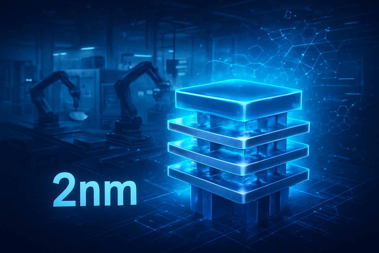
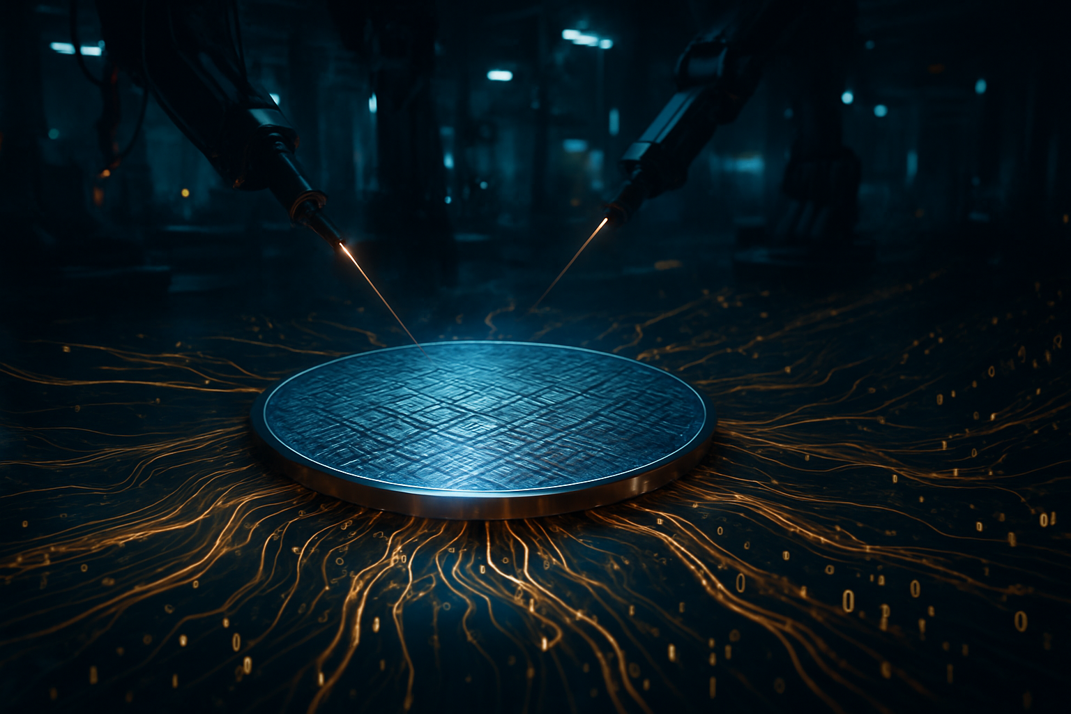
    As of February 2026, the global semiconductor industry has reached a historic inflection point. For over a decade, the FinFET transistor architecture reigned supreme, powering the rise of the smartphone and the cloud. Today, that era is over. We have officially entered the "2nm era," a high-stakes technological frontier where Taiwan Semiconductor Manufacturing Company (NYSE: TSM) and Intel Corporation (NASDAQ: INTC) are locked in a fierce struggle to define the future of high-performance computing and artificial intelligence.

    This month marks a critical milestone in this rivalry. While TSMC has successfully ramped up its N2 (2nm) mass production at its state-of-the-art fabs in Hsinchu and Kaohsiung, Intel has countered with the wide availability of its 18A process, powering the newly launched Panther Lake processor family. For the first time in nearly a decade, the gap between the world’s leading foundry and the American silicon giant has narrowed to a razor’s edge, creating a "duopoly of advanced nodes" that will dictate the performance of every AI model and mobile device for years to come.

    The Architecture of the Future: GAA Nanosheets and PowerVia

    The technical heart of this battle lies in the transition to Gate-All-Around (GAA) transistor technology. TSMC’s N2 node represents the company’s first departure from the traditional FinFET design, utilizing nanosheet transistors that provide superior electrostatic control. By early 2026, yield reports indicate that TSMC has achieved a healthy 65–75% yield on its N2 wafers, offering a 10–15% performance boost or a 30% reduction in power consumption compared to its 3nm predecessors. This efficiency is critical for AI-integrated hardware, where thermal management has become the primary bottleneck.

    Intel, however, has executed a daring "leapfrog" strategy with its 18A node. While TSMC focuses on pure transistor scaling, Intel has introduced PowerVia, its proprietary backside power delivery system. By moving power routing to the back of the wafer, Intel has decoupled power delivery from signal lines, dramatically reducing interference and enabling higher clock speeds. Early benchmarks of the Panther Lake (Core Ultra Series 3) chips, launched in January 2026, show a 50% multi-threaded performance gain over previous generations. Industry experts note that while TSMC still maintains a lead in transistor density—projected at roughly 313 million transistors per square millimeter compared to Intel's 238—Intel’s implementation of backside power has allowed it to match Apple Inc. (NASDAQ: AAPL) in performance-per-watt for the first time in the silicon era.

    Strategic Realignment: Apple, NVIDIA, and the New Foundry Order

    The implications for tech giants are profound. Apple has once again secured its position as TSMC’s premier partner, reportedly consuming over 50% of the initial 2nm capacity for its upcoming A20 and M6 chips. This exclusive access gives Apple a significant lead in the premium smartphone and PC markets, ensuring that the next generation of iPhones remains the gold standard for on-device AI efficiency. However, the landscape is shifting for other major players like NVIDIA Corporation (NASDAQ: NVDA). While NVIDIA remains TSMC’s largest revenue contributor, the company is reportedly bypassing the initial N2 node in favor of TSMC’s upcoming A16 (1.6nm) process, relying on enhanced 3nm nodes for its current "Rubin" AI accelerators.

    Intel’s success with 18A is already disrupting the foundry market. Intel Foundry has successfully courted "whale" customers that were previously exclusive to TSMC. Microsoft Corporation (NASDAQ: MSFT) and Amazon.com, Inc. (NASDAQ: AMZN) have both confirmed they are using the 18A node for their custom AI fabric chips and Maia 3 accelerators. This diversification of the supply chain is a strategic win for US-based tech firms seeking to mitigate geopolitical risks associated with Taiwan-centric manufacturing. Furthermore, the US Department of Defense has officially integrated 18A into its high-performance computing roadmap, cementing Intel’s role as the Western world’s primary domestic source for advanced logic.

    AI Scaling and the Geopolitics of Silicon

    The "2nm battleground" is more than just a race for smaller transistors; it is the physical foundation of the Generative AI revolution. As AI models move from data centers to the "edge"—running locally on laptops and phones—the demand for low-power, high-density silicon has reached a fever pitch. The move to GAA architectures is essential for supporting the massive matrix multiplications required by Large Language Models (LLMs) without draining a device’s battery in minutes.

    However, a new bottleneck has emerged: advanced packaging. While Intel and TSMC are neck-and-neck in wafer fabrication, TSMC maintains a significant advantage with its Chip-on-Wafer-on-Substrate (CoWoS) packaging. NVIDIA currently commands approximately 60% of TSMC’s CoWoS capacity, effectively creating a "moat" that prevents competitors from scaling their AI hardware, regardless of which 2nm node they use. This highlights a broader trend in the AI landscape: the winner of the 2nm era will not just be the company with the best transistors, but the one that can provide a complete, vertically integrated manufacturing ecosystem.

    Looking Ahead: The 1.6nm Horizon and High-NA EUV

    As we look toward the remainder of 2026 and into 2027, the focus is already shifting to the next frontier: 1.6nm. TSMC has accelerated its A16 roadmap to compete with Intel’s 14A node, both of which are expected to utilize High-Numerical Aperture (High-NA) Extreme Ultraviolet (EUV) lithography. These machines, costing upwards of $350 million each, are the rarest and most complex manufacturing tools on Earth. Intel’s early investment in High-NA EUV at its Oregon facility gives it a potential "first-mover" advantage for the sub-2nm generation.

    In the near term, we expect to see the first head-to-head consumer benchmarks between the A20-powered iPhone 18 and Panther Lake-powered laptops in late 2026. The primary challenge for both companies will be sustaining yields as they scale these incredibly complex architectures. If Intel can maintain its 18A momentum, it may finally break TSMC’s near-monopoly on advanced foundry services, leading to a more competitive and resilient global semiconductor market.

    A New Era of Silicon Competition

    The 2nm battle of 2026 marks the end of the "catch-up" phase for Intel and the beginning of a genuine two-way race for silicon supremacy. TSMC remains the undisputed volume king, backed by the immense design prowess of Apple and the manufacturing scale of its Taiwanese "Mega-Fabs." Yet, Intel’s successful rollout of 18A and PowerVia proves that the American giant is once again a formidable contender in the foundry space.

    For the AI industry, this competition is a catalyst for innovation. With two world-class foundries pushing the limits of physics, the rate of hardware advancement is set to accelerate. The coming months will be defined by yield stability, packaging capacity, and the ability of these two titans to meet the insatiable appetite of the AI era. One thing is certain: the 2nm milestone is not the finish line, but the starting gun for a new decade of silicon-driven transformation.


    This content is intended for informational purposes only and represents analysis of current AI developments.

    TokenRing AI delivers enterprise-grade solutions for multi-agent AI workflow orchestration, AI-powered development tools, and seamless remote collaboration platforms.
    For more information, visit https://www.tokenring.ai/.

  • Samsung Cracks the 2nm Code: 70% Yield Milestone for SF2P Challenges TSMC’s Foundry Hegemony

    Samsung Cracks the 2nm Code: 70% Yield Milestone for SF2P Challenges TSMC’s Foundry Hegemony

    In a seismic shift for the global semiconductor landscape, Samsung Electronics (KRX: 005930) has officially reached a 70% yield milestone for its second-generation 2nm Gate-All-Around (GAA) process, known as SF2P. This achievement, confirmed following the company’s recent Q4 2025 performance review, marks the first time a competitor has demonstrated high-volume manufacturing stability on par with the industry’s "golden threshold" for next-generation 2nm nodes. As the world moves deeper into the era of pervasive AI, Samsung’s breakthrough provides the critical supply chain relief and competitive pricing required to sustain the current pace of hardware innovation.

    The significance of this milestone cannot be overstated. For the past three years, the high-performance computing (HPC) and mobile sectors have been effectively tethered to the capacity and pricing whims of TSMC (NYSE: TSM). By stabilizing the SF2P node at 70%, Samsung has not only proven the long-term viability of its early bet on GAA architecture but has also established a credible "dual-sourcing" alternative for the world’s largest chip designers. This development effectively ends the 2nm monopoly before it could truly begin, setting the stage for a high-stakes foundry war in 2026.

    Technical Specifications and the Shift to GAA

    The SF2P process represents the performance-optimized iteration of Samsung’s 2nm roadmap, succeeding the mobile-centric SF2 node. While the first-generation SF2 struggled throughout 2025 with yields hovering in the 50–60% range, the leap to 70% for SF2P is the result of four years of telemetry data harvested from Samsung’s early 3nm GAA deployments. Unlike the traditional FinFET (Fin Field-Effect Transistor) architecture used by TSMC up through its 3nm nodes, Samsung’s Multi-Bridge Channel FET (MBCFET) utilizes nanosheets that allow for finer control over current flow. This architectural lead has finally paid dividends, allowing SF2P to deliver a 12% performance boost and a 25% reduction in power consumption compared to the previous SF3 generation.

    Technical experts in the AI research community are particularly focused on the thermal advantages of the SF2P node. By optimizing the GAA structure, Samsung has successfully addressed the "leakage" issues that plagued earlier sub-5nm attempts. The SF2P node also features an 8% area reduction over SF2, allowing for higher transistor density—a critical requirement for the massive "monolithic" dies used in AI training chips. Industry analysts suggest that this stabilization is a clear sign that the "learning curve" for nanosheet technology has finally been flattened, providing a mature platform for the most demanding silicon designs.

    Initial reactions from the semiconductor industry indicate a mix of relief and cautious optimism. While TSMC still maintains a slight lead with its N2 process yields reportedly touching 80% for early commercial runs, the cost of TSMC’s 2nm wafers—rumored to be near $30,000—has left many designers looking for an exit strategy. Samsung’s ability to offer a 70% yield on a technologically comparable node at a more competitive price point changes the negotiation dynamics for every major fabless firm in the industry.

    Strategic Implications for Chip Designers and Tech Giants

    The stabilization of the SF2P node has immediate and profound implications for tech giants like NVIDIA (NASDAQ: NVDA) and Qualcomm (NASDAQ: QCOM). NVIDIA, which has seen its margins pressured by TSMC’s premium pricing and limited CoWoS (Chip on Wafer on Substrate) packaging capacity, is reportedly in the final stages of performance evaluation for SF2P. By utilizing Samsung as a "release valve" for its next-generation AI accelerators, NVIDIA can diversify its manufacturing risk and ensure that the global AI boom isn't throttled by a single point of failure in the Taiwan Strait.

    For Qualcomm, the news is equally transformative. Reports suggest that a custom version of the Snapdragon 8 Elite Gen 6, slated for 2027, may be produced using Samsung’s 2nm GAA process. This would provide Qualcomm with the strategic leverage needed to push back against TSMC’s annual price hikes while ensuring a steady supply for the next wave of "AI PCs" and premium smartphones. Similarly, Tesla (NASDAQ: TSLA) has already doubled down on its partnership with Samsung, securing a $16.5 billion multiyear deal to manufacture the AI6 chip for its Full Self-Driving (FSD) and Optimus robotics platforms at Samsung’s new facility in Taylor, Texas.

    Startups and mid-tier AI labs are also poised to benefit from this shift. As Samsung increases its 2nm capacity, the "trickle-down" effect will likely result in more affordable access to leading-edge nodes for specialized AI silicon, such as edge inference processors and custom ASICs. The increased competition between Samsung, TSMC, and even Intel (NASDAQ: INTC) with its 18A node, ensures that the price-per-transistor continues to decline, even as the complexity of the designs skyrockets.

    Broader Significance in the AI Landscape

    Looking at the broader AI landscape, Samsung’s 2nm success is a pivotal moment in the hardware-software feedback loop. For years, the industry has feared a "hardware wall" where the cost of manufacturing reached a point of diminishing returns. Samsung’s breakthrough proves that GAA technology is not only feasible but scalable, ensuring that the next generation of Large Language Models (LLMs) and autonomous systems will have the compute density required to reach the next level of intelligence. It mirrors the historic shift from planar transistors to FinFET a decade ago, marking a transition that will define the next ten years of computing.

    However, the rapid advancement of 2nm technology also raises geopolitical and environmental concerns. The immense power required to run 2nm lithography machines and the sheer volume of ultrapure water needed for fabrication remain significant hurdles. Furthermore, while Samsung’s Texas facility offers a geographic hedge against instability in East Asia, the concentration of 2nm expertise remains in the hands of a very small number of players. This "foundry bottleneck" continues to be a point of discussion for regulators who are wary of the systemic risks inherent in the AI supply chain.

    Comparatively, this milestone stands alongside Intel’s early 2010s dominance and TSMC’s 7nm breakthrough as a definitive moment in semiconductor history. It signals that the era of "Single Source Dominance" is fading. With three major players—TSMC, Samsung, and Intel—now competing on the leading edge, the industry is entering its most competitive phase since the early 2000s, which historically has been a period of accelerated technological gains for the end consumer.

    Future Developments: The Road to 1nm and Beyond

    The road ahead for Samsung involves not just maintaining these yields, but iterating on them. The company is already looking toward its SF2Z node, scheduled for 2027, which will introduce Backside Power Delivery Network (BSPDN) technology. This advancement moves the power rails to the back of the wafer, eliminating the bottleneck between power and signal lines that currently limits performance in high-density AI chips. If Samsung can successfully integrate BSPDN while maintaining high yields, they may actually leapfrog TSMC’s performance metrics in the 2027-2028 timeframe.

    Near-term applications for SF2P will likely focus on high-end smartphone SoCs and cloud-based AI training hardware. However, the mid-term horizon suggests that 2nm GAA will become the standard for autonomous vehicles and medical diagnostics hardware, where power efficiency is a life-or-death specification. The challenge for Samsung now lies in its Advanced Packaging (AVP) capabilities; the silicon is only half the battle, and the company must prove it can package these 2nm dies as effectively as TSMC’s world-class 3D-IC solutions.

    Experts predict that the focus of 2026 will shift from "can it be made?" to "how many can be made?" The battle for 2nm supremacy will be won in the logistics and capacity expansion phases. As Samsung ramps up its Taylor, Texas and Pyeongtaek fabs, the industry will be watching closely to see if the 70% yield remains stable at high volumes. If it does, the balance of power in the tech world will have shifted irrevocably.

    Conclusion: A New Era of Competition

    Samsung’s 70% yield milestone for SF2P is more than just a corporate achievement; it is a stabilizing force for the entire global technology economy. By proving that 2nm GAA can be produced reliably and at scale, Samsung has provided a roadmap for the future of AI hardware that is no longer dependent on a single manufacturer. The key takeaways are clear: the technical barrier to 2nm has been breached, the cost of high-end silicon is likely to stabilize due to increased competition, and the architectural shift to GAA is now the industry standard.

    In the grand arc of AI history, this development will likely be remembered as the moment the hardware supply chain caught up with the software's ambitions. It ensures that the "AI era" has the foundational infrastructure it needs to grow without being constrained by manufacturing scarcity. For investors and tech enthusiasts alike, the next few months will be critical as we see the first commercial silicon from these 2nm wafers hit the testing benches.

    What to watch for in the coming weeks and months: official "tape-out" announcements from NVIDIA and Qualcomm, updates on the operational status of Samsung’s Taylor, Texas fab, and TSMC’s pricing response to this newfound competition. The foundry wars have entered a new, more intense chapter, and the beneficiaries are the developers and users of the next generation of artificial intelligence.


    This content is intended for informational purposes only and represents analysis of current AI developments.

    TokenRing AI delivers enterprise-grade solutions for multi-agent AI workflow orchestration, AI-powered development tools, and seamless remote collaboration platforms.
    For more information, visit https://www.tokenring.ai/.

  • The Silicon Throne: TSMC’s Record $56B Bet on the Future of Artificial Intelligence

    The Silicon Throne: TSMC’s Record $56B Bet on the Future of Artificial Intelligence

    In a move that underscores the sheer scale of the ongoing generative artificial intelligence revolution, Taiwan Semiconductor Manufacturing Company (NYSE:TSM) has officially announced a record-breaking $56 billion capital expenditure plan for 2026. This historic investment, disclosed during the company’s recent Q1 earnings briefing, marks the largest single-year spending commitment in the history of the semiconductor industry. As the world’s leading foundry, TSMC is signaling its absolute confidence that the demand for high-performance computing (HPC) will continue to accelerate, fueled by the insatiable needs of AI hyperscalers and chip designers.

    The significance of this announcement extends far beyond simple infrastructure. TSMC has projected a massive 30% revenue growth for the fiscal year 2026, a figure that has sent shockwaves through global markets. By allocating over 80% of its budget to advanced nodes and specialized packaging, TSMC is not just building more factories; it is constructing the physical bedrock upon which the next decade of AI breakthroughs—including autonomous systems, massive-scale LLMs, and personalized digital agents—will be built.

    Scaling the Impossible: 2nm and the Rise of A16 Architecture

    The technical core of TSMC’s 2026 strategy lies in the aggressive ramp-up of its 2nm (N2) process and the introduction of the groundbreaking A16 (1.6nm) node. The N2 process, which is now hitting mass production across TSMC’s facilities in Baoshan and Kaohsiung, represents a paradigm shift in transistor design. For the first time, TSMC is utilizing Gate-All-Around (GAA) nanosheet transistors. Unlike the previous FinFET architecture, GAA allows for better electrostatic control, resulting in a 10-15% performance boost or a 25-30% reduction in power consumption compared to the 3nm node.

    Complementing the 2nm rollout is the A16 node, scheduled for volume production in the second half of 2026. The A16 is being hailed by industry experts as the "crown jewel" of TSMC’s roadmap because it introduces the "Super Power Rail." This backside power delivery system moves power distribution from the front of the wafer to the back, freeing up critical space on the top layers for signal routing. This technical leap effectively eliminates bottlenecks in power delivery that have plagued high-wattage AI accelerators, allowing for even higher clock speeds and more efficient thermal management.

    Initial reactions from the semiconductor research community suggest that TSMC has successfully widened its lead over rivals Intel (NASDAQ:INTC) and Samsung. While Intel has made strides with its 18A process, TSMC’s ability to achieve volume production with A16 while maintaining nearly 50% net margins is viewed as a masterstroke in manufacturing execution. "We are no longer just looking at incremental shrinks," said one senior analyst at the Semiconductor Industry Association. "TSMC is re-engineering the very physics of how electricity moves through a chip to meet the thermal demands of the AI era."

    The NVIDIA and Meta Connection: Powering the AI Super-Cycle

    This $56 billion investment is a direct response to the "AI Super-Cycle" led by tech giants like NVIDIA (NASDAQ:NVDA) and Meta (NASDAQ:META). NVIDIA, which has officially overtaken Apple (NASDAQ:AAPL) as TSMC’s largest customer, is the primary driver for the 2026 capacity surge. NVIDIA’s upcoming "Rubin" architecture, the successor to the Blackwell GPUs, is slated to transition to TSMC’s 3nm (N3P) and eventually 2nm nodes. To satisfy NVIDIA’s roadmap, TSMC is also doubling down on its CoWoS (Chip on Wafer on Substrate) advanced packaging capacity, which remains the primary bottleneck for shipping enough AI chips to meet global demand.

    Meta’s role in this expansion is equally pivotal. Mark Zuckerberg’s company has emerged as a top-tier TSMC client, securing massive allocations for its custom Meta Training and Inference Accelerator (MTIA) chips. As Meta continues its pivot toward "General AI" and integrates advanced intelligence across its social platforms, its reliance on bespoke silicon has made it a key strategic partner in TSMC’s long-term planning. For Meta, securing TSMC’s A16 capacity early is a competitive necessity to ensure its future models can out-compute rivals in a high-latency-sensitive environment.

    The market positioning here is clear: TSMC has created a "virtuous cycle" where the world’s most powerful software companies are effectively subsidizing the development of the world’s most advanced hardware. This creates a formidable barrier to entry for smaller firms and even legacy tech giants. Companies that do not have "priority access" to TSMC’s 2nm and A16 nodes in 2026 risk falling an entire generation behind in compute efficiency, which in the AI world translates directly to higher costs and slower innovation.

    Geopolitics and the Global Fab Cluster Strategy

    The $56 billion plan is not just about technology; it is about geographical resilience. TSMC is currently transforming its manufacturing footprint into "Megafab Clusters" located in the United States, Japan, and Germany. In Arizona, Fab 1 is now fully operational at the 4nm node, while the mass production timeline for Fab 2 has been accelerated to late 2027 to handle 3nm and 2nm chips. This expansion is critical for US-based partners like AMD (NASDAQ:AMD) and NVIDIA, who are increasingly under pressure to diversify their supply chains amidst ongoing geopolitical tensions in the Taiwan Strait.

    However, this global expansion brings its own set of challenges. Critics have pointed to the rising costs of manufacturing outside of Taiwan, where TSMC benefits from a highly specialized local ecosystem. To maintain its 30% revenue growth target, TSMC has had to implement "regional pricing" models, charging a premium for chips made in US-based fabs. Despite these costs, the "AI gold rush" has made customers willing to pay for the security of supply.

    Comparatively, this milestone echoes the early 2010s mobile revolution, but at a significantly larger scale. While the shift to smartphones redefined consumer tech, the current AI infrastructure build-out is fundamental to the entire global economy. The concern among some economists is the potential for an "over-investment" bubble; however, with TSMC’s order books for 2026 and 2027 already reported as "fully booked," the immediate threat appears to be a lack of capacity rather than a surplus.

    Looking Ahead: The Road to Sub-1nm

    As 2026 unfolds, the industry is already looking toward the next frontier. TSMC has hinted at a "1nm-class" node research phase, potentially designated as the A14 or A10, which will likely integrate even more exotic materials like carbon nanotubes or two-dimensional semiconductors. In the near term, the focus will remain on the successful integration of High-NA EUV (High Numerical Aperture Extreme Ultraviolet) lithography machines, which are essential for printing the incredibly fine features required for the A16 node.

    The primary challenges moving forward are no longer just about lithography. Power and water consumption for these mega-facilities have become significant political and environmental hurdles. In Taiwan, TSMC is investing heavily in water reclamation plants and renewable energy to ensure its 2nm ramp-up does not strain local resources. In Arizona, the focus is on building out a local talent pipeline of specialized engineers to staff the three planned facilities.

    Experts predict that by the end of 2026, the gap between TSMC and its competitors will be defined not just by transistor density, but by "system-level" integration. This involves 3D stacking of logic and memory (SoIC), which TSMC is rapidly scaling. The future of AI is moving toward "Silicon-as-a-Service," where TSMC provides the entire compute package—not just the chip.

    A New Era of Silicon Sovereignty

    TSMC’s $56 billion commitment for 2026 is a definitive statement that the AI era is still in its infancy. By betting nearly 30% of its projected revenue back into R&D and capital projects, the company is ensuring its role as the indispensable middleman of the digital age. The key takeaways for 2026 are clear: the transition to 2nm and A16 architecture is the new battlefield for AI supremacy, and NVIDIA and Meta have secured their positions at the front of the line.

    As we move through the coming months, the tech world will be watching the yield rates of the new A16 node and the progress of the Arizona Fab 2 construction. This investment represents more than just a business plan; it is the most expensive and complex engineering project in human history, designed to power the next generation of human intelligence. In the high-stakes game of semiconductor manufacturing, TSMC has just raised the stakes to an unprecedented level, and the rest of the world has no choice but to follow.


    This content is intended for informational purposes only and represents analysis of current AI developments.

    TokenRing AI delivers enterprise-grade solutions for multi-agent AI workflow orchestration, AI-powered development tools, and seamless remote collaboration platforms.
    For more information, visit https://www.tokenring.ai/.

  • Samsung Taylor Fab Commences Risk Production for 2nm Chips

    Samsung Taylor Fab Commences Risk Production for 2nm Chips

    In a move that signals a seismic shift in the global semiconductor landscape, Samsung Electronics (KRX: 005930) has officially commenced risk production for its 2nm (SF2) process node at its $44 billion facility in Taylor, Texas. This milestone marks the first time that cutting-edge 2nm-class silicon has been manufactured on U.S. soil, representing a critical victory for Samsung in its bid to challenge the dominance of Taiwan Semiconductor Manufacturing Company (TPE: 2330).

    The Taylor facility, which has transitioned from its original 4nm mandate to a "2nm-first" strategy, is now operating its first batch of advanced lithography systems. This development is not merely a technical achievement; it is a foundational pillar of the U.S. strategy to secure domestic leading-edge chip production. Supported by $6.4 billion in subsidies from the CHIPS and Science Act, Samsung’s Texas operations are now the epicenter of a "Turnkey" manufacturing ecosystem designed to provide the world’s most advanced AI hardware under one roof.

    Technical Prowess: Third-Generation GAA and CNT Pellicles

    The 2nm process, designated as SF2 by Samsung Foundry, utilizes the third generation of the company’s proprietary Gate-All-Around (GAA) architecture, branded as Multi-Bridge Channel FET (MBCFET). While competitors like TSMC are just beginning their transition to GAA at the 2nm level, Samsung is leveraging nearly four years of telemetry data from its early 3nm GAA production. The SF2 node delivers a 12% increase in performance and a 25% reduction in power consumption compared to the previous 3nm generation. This efficiency is critical for the next wave of hyperscale AI accelerators and mobile processors that are pushing the limits of thermal management.

    A key differentiator in the Taylor fab’s 2nm line is the large-scale implementation of advanced Extreme Ultraviolet (EUV) pellicles. Samsung has adopted Carbon Nanotube (CNT) pellicle technology, which boasts a light transmittance rate exceeding 97%. This is a significant upgrade over traditional silicon-based pellicles, which often suffer from lower transparency and thermal degradation under the high-power EUV beams required for 2nm patterning. By reducing "stochastic" defects and increasing wafer throughput, these CNT pellicles are expected to help Samsung achieve a target yield of 60-70%—a figure that would make it highly competitive with TSMC’s N2 node.

    Furthermore, Samsung is preparing its SF2P (Performance) variant for high-end data center applications, which features specialized channel strain engineering to reduce parasitic capacitance. Initial reactions from the industry have been cautiously optimistic; while Samsung struggled with early 3nm yields, the stabilization of its 2nm process in Taylor suggests that the company has finally overcome the learning curve associated with GAA structures.

    Market Dynamics: Courting AMD, Qualcomm, and Tesla

    Samsung’s strategic pivot to the United States is already paying dividends in terms of customer acquisition. Advanced Micro Devices (NASDAQ: AMD) and Qualcomm (NASDAQ: QCOM) are reportedly in deep negotiations to secure 2nm capacity at the Taylor fab. For Qualcomm, the attraction lies in Samsung’s ability to offer a "dual-sourcing" alternative to TSMC, where Apple has reportedly reserved the lion's share of initial 2nm capacity. Industry insiders suggest that Samsung’s 2nm wafers could be priced as much as 33% lower than TSMC’s, providing a vital margin cushion for chip designers facing rising manufacturing costs.

    The Taylor fab has also secured a cornerstone client in Tesla (NASDAQ: TSLA). The electric vehicle giant is expected to use the facility for its next-generation AI6 autonomous driving chips. By fabbing these chips in Texas, Tesla gains a localized supply chain that minimizes geopolitical risk and logistical overhead. This "Made in USA" advantage is becoming a primary selling point as tech giants look to diversify their manufacturing footprint away from East Asia.

    The competitive landscape is further complicated by Intel (NASDAQ: INTC), which has recently ramped up its 18A node. While Intel currently holds a lead in backside power delivery technology, Samsung’s "Turnkey Strategy"—which integrates 2nm logic, HBM4 memory, and advanced 3D packaging (SAINT)—offers a comprehensive solution that Intel and TSMC struggle to match individually. This holistic approach is particularly attractive to AI startups and hyperscalers that require high-bandwidth memory to be stacked directly onto 2nm logic dies.

    Geopolitics and the AI Hardware Explosion

    The commencement of 2nm risk production in Taylor is a landmark moment in the broader AI landscape. As the demand for NVIDIA (NASDAQ: NVDA) GPUs and custom AI ASICs continues to outpace supply, the addition of a major 2nm hub in the United States provides a necessary safety valve for the industry. It aligns perfectly with the current trend toward sovereign AI, where nations and corporations seek to control their hardware destiny.

    This development also underscores the success of the CHIPS Act in incentivizing leading-edge manufacturing within the U.S. The Taylor campus, now a $44 billion investment, represents one of the largest foreign direct investments in U.S. history. By fostering a "K-Semiconductor Cluster" in Central Texas—including specialized suppliers for EUV pellicles and materials—Samsung is building an ecosystem that will likely influence semiconductor trends for the next decade.

    However, concerns remain regarding the speed of the yield ramp. While 60% yield is a strong start for 2nm, the industry standard for high-volume profitability typically requires upwards of 70-80%. Comparisons to previous milestones, such as the move from 7nm to 5nm, show that the transition to 2nm is orders of magnitude more complex due to the extreme precision required in lithography and the fragility of nanosheet structures.

    The Horizon: From Risk Production to 1.4nm

    Looking ahead, Samsung plans to transition from risk production to full-scale mass production at the Taylor fab by the second half of 2026. This timeline puts them in a neck-and-neck race with TSMC’s Arizona facility. In the near term, we can expect to see the first 2nm-powered consumer devices, likely headlined by Samsung's own Galaxy S27 series and potentially a refreshed line of AI-capable laptops from various OEMs.

    Beyond 2nm, Samsung has already laid out a roadmap for its 1.4nm (SF1.4) node, which is slated for development by late 2027. The Taylor fab is designed to be future-proof, with the infrastructure already in place to support the move to "High-NA" EUV systems from ASML (NASDAQ: ASML) as they become commercially viable. The primary challenge moving forward will be the integration of Backside Power Delivery (BSPDN) in the SF2Z variant, which experts predict will be the next major battleground in semiconductor architecture.

    A Final Assessment of the Taylor Milestone

    The commencement of 2nm risk production at Samsung’s Taylor fab is a definitive "coming of age" moment for the U.S. semiconductor industry and a bold statement of intent from Samsung. By combining its 3rd-generation GAA technology with a multi-billion dollar commitment to American manufacturing, Samsung is not just building a factory; it is attempting to rewrite the rules of the foundry market.

    The significance of this development in AI history cannot be overstated. As AI models become more complex, the hardware that powers them must become more efficient and accessible. The Taylor facility provides the capacity and the cutting-edge tech to meet that demand. In the coming weeks and months, the industry will be watching Samsung’s yield reports and customer announcements closely. If the company can maintain its current momentum, the "Silicon Hills" of Texas may soon become the most important real estate in the global AI economy.


    This content is intended for informational purposes only and represents analysis of current AI developments.

    TokenRing AI delivers enterprise-grade solutions for multi-agent AI workflow orchestration, AI-powered development tools, and seamless remote collaboration platforms.
    For more information, visit https://www.tokenring.ai/.

  • Silicon’s New Horizon: TSMC Hits 2nm Milestone as GAA Transition Reshapes AI Hardware

    Silicon’s New Horizon: TSMC Hits 2nm Milestone as GAA Transition Reshapes AI Hardware

    As of January 30, 2026, the global semiconductor landscape has officially entered the "Angstrom Era." Taiwan Semiconductor Manufacturing Company (NYSE: TSM), the world's largest contract chipmaker, has successfully transitioned its 2nm (N2) process from pilot lines to high-volume manufacturing (HVM). This milestone represents more than just a reduction in feature size; it marks the most significant architectural overhaul in semiconductor design since the introduction of FinFET over a decade ago.

    The immediate significance of the N2 node cannot be overstated, particularly for the burgeoning artificial intelligence sector. With production now scaling at TSMC's Baoshan and Kaohsiung facilities, the first wave of 2nm-powered devices is expected to hit the market by the end of the year. This shift provides the critical hardware foundation required to sustain the massive compute demands of next-generation large language models and autonomous systems, effectively extending the lifespan of Moore’s Law through sheer architectural ingenuity.

    The Nanosheet Revolution: Engineering the 2nm Breakthrough

    The technical centerpiece of the N2 node is the transition from the long-standing FinFET (Fin Field-Effect Transistor) architecture to Gate-All-Around (GAA) technology, which TSMC refers to as "Nanosheet" transistors. In previous FinFET designs, the gate covered three sides of the channel. However, as transistors shrunk toward the 2nm limit, electron leakage became an insurmountable hurdle. The Nanosheet design solves this by wrapping the gate entirely around the channel on all four sides. This provides superior electrostatic control, virtually eliminating current leakage and allowing for significantly lower operating voltages.

    Beyond the transistor geometry, TSMC has introduced a proprietary feature known as NanoFlex™. This technology allows chip designers at firms like Apple (NASDAQ: AAPL) and NVIDIA (NASDAQ: NVDA) to mix and match different standard cell types—short cells for power efficiency and tall cells for peak performance—on a single die. This granular control over the power-performance-area (PPA) profile is unprecedented. Early reports from January 2026 indicate that TSMC has achieved logic test chip yields between 70% and 80%, a remarkable feat that places them well ahead of competitors like Samsung (KRX: 005930), whose 2nm GAA yields are reportedly struggling in the 40-55% range.

    In terms of raw performance, the N2 process is delivering a 10% to 15% speed increase at the same power level compared to the refined 3nm (N3E) process. Perhaps more importantly for mobile and edge AI applications, it offers a 25% to 30% reduction in power consumption at the same clock speed. This efficiency gain is the primary driver for the massive industry interest, as it allows for more complex AI processing to occur on-device without devastating battery life or thermal envelopes.

    The 2026 Capacity Crunch: Apple and NVIDIA Lead the Charge

    The scramble for 2nm capacity has created a "supply choke" that has defined the early months of 2026. Industry insiders confirm that TSMC’s N2 capacity is effectively fully booked through the end of the year, with Apple and NVIDIA emerging as the dominant stakeholders. Apple has reportedly secured over 50% of the initial 2nm output, which it plans to utilize for its upcoming A20 Bionic chips in the iPhone 18 series and the M6 series processors for its MacBook Pro and iPad Pro lineups. For Apple, this exclusivity ensures that its "Apple Intelligence" ecosystem remains the gold standard for on-device AI performance.

    NVIDIA has also made an aggressive play for 2nm wafers to power its "Rubin" GPU platform. As generative AI workloads continue to grow exponentially, NVIDIA’s move to 2nm is seen as a strategic necessity to maintain its dominance in the data center. By moving to the N2 node, NVIDIA can pack more CUDA cores and specialized AI accelerators into a single chip while staying within the power limits of modern liquid-cooled server racks. This has placed smaller AI startups and rival chipmakers in a precarious position, as they must compete for the remaining "leftover" capacity or wait for the 2nm ramp-up to reach 140,000 wafers per month by late 2026.

    The cost of this technological edge is steep. Wafers for the 2nm process are currently estimated at $30,000 each, a 20% premium over the 3nm generation. This pricing reinforces a "winners-take-all" market dynamic, where only the wealthiest tech giants can afford the most advanced silicon. For consumers, this likely translates to higher price points for flagship hardware, but for the industry, it represents the massive capital expenditure required to keep the AI revolution moving forward.

    Redefining the AI Landscape: Sustainability and Sovereignty

    The shift to 2nm has implications that reach far beyond faster smartphones. In the broader AI landscape, the improved power efficiency of N2 is a critical component of the industry’s "green AI" initiatives. As data centers consume an ever-increasing percentage of global electricity, the 30% power reduction offered by 2nm chips becomes a vital tool for sustainability. This allows major cloud providers to expand their AI training clusters without requiring a linear increase in energy infrastructure, mitigating some of the environmental concerns surrounding the AI boom.

    Furthermore, the 2nm milestone solidifies TSMC’s role as the indispensable lynchpin of the global digital economy. As the only foundry currently capable of delivering high-yield 2nm GAA wafers at scale, TSMC’s technological lead has become a matter of national and corporate sovereignty. This has intensified the competitive pressure on Intel (NASDAQ: INTC) and Samsung to accelerate their own roadmaps. While Intel’s 18A process is beginning to gain traction, TSMC’s successful N2 rollout in early 2026 suggests that the "Taiwan Advantage" remains firmly in place for the foreseeable future.

    However, the concentration of 2nm manufacturing in Taiwan remains a point of strategic anxiety for global markets. Despite TSMC’s expansion into Arizona and Japan, the most advanced 2nm "GigaFabs" are currently concentrated in Hsinchu and Kaohsiung. This geopolitical reality means that any disruption in the region would immediately halt the production of the world’s most advanced AI and consumer chips, a vulnerability that continues to drive investments in domestic chip manufacturing in the U.S. and Europe.

    The Road to 1.6nm: Super PowerRail and the A16 Era

    Even as N2 production ramps up, TSMC is already looking toward its next major leap: the A16 (1.6nm) node. Scheduled for high-volume manufacturing in the second half of 2026, A16 will introduce "Super PowerRail" (SPR) technology. This is TSMC’s proprietary implementation of a Backside Power Delivery Network (BSPDN). Traditionally, power and signal lines are bundled on the front side of a wafer. SPR moves the power delivery to the back, connecting it directly to the transistor's source and drain.

    This innovation is expected to free up nearly 20% more space for signal routing on the front side, significantly reducing "IR drop" (voltage loss) and improving power delivery efficiency. Experts predict that A16 will provide an additional 8% to 10% speed boost over N2P (the performance-enhanced version of 2nm). However, moving the power network to the backside presents a new set of thermal management challenges, as the chip's ability to spread heat laterally is reduced. This will likely necessitate new cooling solutions, such as microfluidic channels integrated directly into the chip packaging.

    Looking ahead, the successful deployment of Super PowerRail in the A16 process will be the defining technical challenge of 2027. If TSMC can solve the thermal hurdles associated with backside power, it will pave the way for chips that are not only smaller but fundamentally more efficient at handling the high-intensity, continuous compute required for real-time AI reasoning and 8K holographic rendering.

    Conclusion: A New Era of Silicon Dominance

    TSMC’s 2nm production milestone is a watershed moment in the history of computing. By successfully navigating the transition from FinFET to Nanosheet architecture, the company has provided the world’s leading technology companies with the tools needed to push AI beyond current limitations. The fact that 2026 capacity is already spoken for by Apple and NVIDIA underscores the desperate industry-wide need for more efficient, more powerful silicon.

    As we move through the first quarter of 2026, the key metrics to watch will be the continued stabilization of N2 yields and the first real-world benchmarks from 2nm-equipped devices. While the A16 roadmap and Super PowerRail technology promise even greater gains, the current focus remains on the flawless execution of N2. For the AI industry, the message is clear: the hardware bottleneck is widening, but the price of entry into the elite tier of performance has never been higher. TSMC's achievement ensures that the momentum of the AI era continues unabated, firmly establishing the 2nm node as the backbone of the next generation of digital innovation.


    This content is intended for informational purposes only and represents analysis of current AI developments.

    TokenRing AI delivers enterprise-grade solutions for multi-agent AI workflow orchestration, AI-powered development tools, and seamless remote collaboration platforms.
    For more information, visit https://www.tokenring.ai/.

  • Samsung Hits 70% Yield on 2nm GAA (SF2P): A Turning Point for the AI Chip Supply Chain

    Samsung Hits 70% Yield on 2nm GAA (SF2P): A Turning Point for the AI Chip Supply Chain

    As of January 30, 2026, the global semiconductor landscape is undergoing a tectonic shift. Samsung Electronics (KRX: 005930) has officially reached a critical performance and yield milestone for its 2nm (SF2P) production process, signaling a major challenge to the long-standing dominance of Taiwan Semiconductor Manufacturing Company (NYSE: TSM). Following its Q4 2025 earnings report, Samsung confirmed that its performance-optimized 2nm node, known as SF2P, has successfully hit the 70% yield threshold required for stable mass production—a feat that many industry skeptics thought would take years to master.

    This development is more than just a technical victory; it is a strategic lifeline for the world’s largest chip designers. With TSMC’s 2nm capacity currently overwhelmed by exclusive orders from high-priority clients, the emergence of a viable, high-yield alternative from Samsung provides a release valve for a supply chain that has been dangerously bottlenecked. By mastering the intricate Gate-All-Around (GAA) architecture ahead of its rivals, Samsung is positioning itself as the primary destination for the next generation of high-performance AI and mobile processors.

    Engineering the Future: The Maturity of 3rd-Gen GAA

    The SF2P node represents the second generation of Samsung’s 2nm platform, specifically optimized for high-performance computing (HPC) and premium mobile devices. Unlike traditional FinFET transistors, which hit physical scaling limits years ago, Samsung’s 2nm utilizes its proprietary Multi-Bridge Channel FET (MBCFET) architecture—a 3rd-generation evolution of GAA technology. This approach allows for a "nanosheet" design where the width of the channel can be adjusted to optimize for either extreme power efficiency or maximum performance. Compared to the first-generation SF2 node, the 2026-era SF2P delivers a 12% boost in clock speeds, a 25% improvement in power efficiency, and an 8% reduction in total die area.

    Technical experts note that Samsung’s early gamble on GAA—which it first introduced at the 3nm node while TSMC stuck with FinFET—is finally paying dividends. While competitors are only now navigating the "learning curve" of nanosheet production, Samsung has accumulated four years of telemetry data on GAA manufacturing. This experience has allowed the foundry to refine its extreme ultraviolet (EUV) lithography processes and address the "stochastic" defects that typically plague sub-3nm nodes. The result is a more uniform transistor structure that significantly reduces leakage current, a critical requirement for the power-hungry AI workloads of 2026.

    A Strategic Pivot: Qualcomm and AMD Secure Capacity

    The immediate beneficiaries of Samsung’s yield breakthrough are Qualcomm (NASDAQ: QCOM) and AMD (NASDAQ: AMD). As of late January 2026, both companies are reportedly in final negotiations to shift significant portions of their 2nm roadmap to Samsung Foundry. The move is driven by a stark reality: TSMC’s 2nm (N2) capacity is nearly 50% reserved by a single customer, leaving other tech giants fighting for leftovers and paying a "wafer premium" that has risen 50% over previous generations. Qualcomm is expected to utilize SF2P for its next-generation Snapdragon series, while AMD is eyeing the node for its "Venice" EPYC server CPUs to ensure supply stability in the face of skyrocketing enterprise demand.

    This shift represents a significant competitive disruption. For years, TSMC’s "foundry-only" model gave it a reputation for neutrality and reliability that Samsung, a conglomerate that also makes its own consumer products, struggled to match. However, the sheer scale of the AI boom has forced a "dual-sourcing" strategy among major chip designers. By offering competitive yields and more favorable pricing than TSMC, Samsung is transforming the foundry market from a monopoly into a true duopoly. Furthermore, Samsung’s massive $16.5 billion contract with Tesla (NASDAQ: TSLA) for its AI6 autonomous driving chips has served as a powerful "seal of approval," encouraging other automotive and data center players to reconsider their reliance on a single supplier.

    The "One-Stop" AI Solution and the Taylor, Texas Factor

    Samsung’s 2nm success is part of a broader "total solution" strategy that integrates logic, memory, and packaging. In January 2026, Samsung began large-scale shipments of its 12-layer HBM4 (High Bandwidth Memory), a key component for AI accelerators used by NVIDIA (NASDAQ: NVDA) and others. By offering 2nm logic manufacturing alongside HBM4 and advanced X-Cube 3D packaging, Samsung provides a vertically integrated stack that reduces latency and power consumption. This "one-stop shop" capability is something neither TSMC nor Intel (NASDAQ: INTC) can currently match with the same level of internal synchronization, making Samsung an attractive partner for startups building custom "Agentic AI" silicon.

    The geopolitical dimension of this ramp-up cannot be ignored. Samsung’s Taylor, Texas facility is now 93% complete and is transitioning to a "2nm-first" factory. With trial runs of ASML EUV lithography tools scheduled for March 2026, the Taylor fab is set to become a cornerstone of the "Made in USA" advanced chip initiative. This domestic capacity is a major selling point for U.S.-based companies like AMD and Google, who are under increasing pressure to diversify their manufacturing away from the geopolitical sensitivities of the Taiwan Strait. Samsung’s ability to hit 70% yield in its Korean facilities provides the blueprint for a rapid and successful ramp in the United States.

    Looking Ahead: The Road to 1.4nm and Backside Power

    While the industry focuses on the SF2P ramp, Samsung’s R&D teams are already moving toward the next frontier. Near-term developments include the introduction of SF2Z in 2027, which will incorporate Backside Power Delivery Network (BSPDN) technology. This innovation moves the power circuitry to the back of the wafer, freeing up the top side for more transistors and further reducing voltage drops. Beyond 2nm, the roadmap points toward the 1.4nm (SF1.4) node, where Samsung expects to apply lessons from its GAA maturity to achieve even more aggressive density gains.

    The challenge remains in maintaining these yields as the volume scales to hundreds of thousands of wafers per month. Experts predict that the next 12 months will be a "volume war" as Samsung attempts to match the total output capacity of TSMC’s sprawling "GigaFabs." Additionally, as AI models move from data centers to "on-device" edge environments, the demand for SF2P-class chips will expand into a wider variety of form factors, including wearable AR glasses and advanced robotics. The primary hurdle will be the continued availability of high-NA EUV tools and the specialized gases required for sub-2nm etching.

    A New Era for the Semiconductor Industry

    Samsung’s achievement of 70% yield on the SF2P node marks a historic comeback for the South Korean giant. After years of trailing TSMC in the transition from 7nm to 5nm and 4nm, Samsung has utilized the radical architecture shift of Gate-All-Around to leapfrog its competition in terms of manufacturing maturity. This development effectively breaks the "TSMC bottleneck," providing the global AI industry with the diversified supply chain it desperately needs to sustain its current pace of innovation.

    In the coming weeks, the industry will be watching for the official "tape-out" announcements from Qualcomm and AMD, which will confirm the first commercial products to use this new technology. The successful integration of SF2P into the global supply chain will not only redefine Samsung’s financial trajectory but will also serve as a catalyst for more affordable and efficient AI hardware worldwide. As we move deeper into 2026, the foundry race has officially been reset, and for the first time in a decade, the lead is up for grabs.


    This content is intended for informational purposes only and represents analysis of current AI and semiconductor developments.

    TokenRing AI delivers enterprise-grade solutions for multi-agent AI workflow orchestration, AI-powered development tools, and seamless remote collaboration platforms.
    For more information, visit https://www.tokenring.ai/.

  • Silicon’s Next Giant Leap: TSMC Commences High-Volume 2nm Production as the Global AI Arms Race Intensifies

    Silicon’s Next Giant Leap: TSMC Commences High-Volume 2nm Production as the Global AI Arms Race Intensifies

    In a move that signals a tectonic shift in the global semiconductor landscape, Taiwan Semiconductor Manufacturing Company (TSMC) (NYSE: TSM) has officially entered high-volume manufacturing (HVM) for its N2 (2-nanometer) technology node as of January 2026. This milestone, centered at the company’s massive Fab 20 facility in Hsinchu’s Baoshan District, marks the first commercial deployment of Nanosheet Gate-All-Around (GAA) transistors—a radical departure from the FinFET architecture that has dominated the industry for over a decade.

    The commencement of N2 production is not merely a routine upgrade; it is the cornerstone of the next generation of artificial intelligence. As the world’s most advanced foundry ships its first batch of 2nm silicon to lead customers like Apple (NASDAQ: AAPL) and NVIDIA (NASDAQ: NVDA), the implications for AI efficiency and compute density are profound. With initial yields reportedly exceeding internal targets, the 2nm era has moved from the laboratory to the factory floor, promising to redefine the performance-per-watt metrics that govern the future of data centers and edge devices alike.

    The Nanosheet Revolution: Inside the Architecture of N2

    The transition to N2 represents the most significant technical hurdle TSMC has cleared since the introduction of FinFET at the 22nm node. Unlike the "fin" structure where the gate wraps around three sides of the channel, the Nanosheet GAA architecture allows the gate to completely surround the channel on all four sides. This "Gate-All-Around" configuration provides superior electrostatic control, which is essential for managing the current leakage that plagued previous nodes at smaller scales. By drastically reducing this "leakage power," TSMC has achieved a staggering 25% to 30% improvement in power efficiency compared to the N3E (3nm) node at the same speed.

    Beyond raw efficiency, N2 introduces a breakthrough "NanoFlex" technology. This capability allows chip designers to mix and match different nanosheet cell types—some optimized for high-density and others for high-performance—within a single chip layout. This granular control is particularly vital for AI accelerators and mobile processors, where different sections of the silicon must handle radically different workloads simultaneously. Initial reactions from the hardware engineering community have been overwhelmingly positive, with experts noting that the 10% to 15% speed increase at constant power will allow the next generation of smartphones to run complex, on-device Large Language Models (LLMs) without the thermal throttling that hampered 3nm devices.

    Production is currently anchored at Fab 20 in Hsinchu, often referred to as TSMC’s "mother fab" for the 2nm era. The facility is a marvel of modern engineering, utilizing the latest Extreme Ultraviolet (EUV) lithography tools with high numerical aperture (High-NA) capabilities being phased in for future iterations. While the N2 node currently utilizes traditional front-side power delivery, it lays the groundwork for the N2P and A16 (1.6nm) nodes, which will eventually introduce backside power delivery to further optimize signal integrity and power distribution.

    The 2nm Race: Competitive Dynamics and Market Hegemony

    The start of N2 HVM places TSMC in a fierce "three-way sprint" against Intel (NASDAQ: INTC) and Samsung (KRX: 005930). While Intel recently claimed it reached HVM for its 18A (1.8nm) node in late 2025, TSMC’s N2 is widely viewed by industry analysts as the "gold standard" for yield and reliability. Intel’s 18A employs a similar RibbonFET architecture and has taken an aggressive lead by integrating "PowerVia" backside power delivery early. However, TSMC’s massive ecosystem of IP partners and its established track record of delivering millions of wafers to Apple give it a strategic moat that competitors struggle to breach.

    The primary beneficiaries of this rollout are the titans of the AI and mobile sectors. Apple has reportedly secured the vast majority of the initial N2 capacity for its upcoming "A20" chips, which will likely power the next iteration of the iPhone. For NVIDIA, the shift to 2nm is critical for its Blackwell successors and future AI GPUs, where every percentage point of power efficiency translates into billions of dollars in savings for hyperscale data center operators like Microsoft (NASDAQ: MSFT) and Amazon (NASDAQ: AMZN). By maintaining its lead in HVM, TSMC reinforces its position as the indispensable bottleneck—and enabler—of the global AI economy.

    Samsung, meanwhile, is attempting to pivot by moving its 2nm production to its new facility in Taylor, Texas. This move is designed to capture the growing demand for "on-shore" manufacturing in the United States. However, with TSMC’s Fab 20 now pumping out 2nm wafers at scale in Taiwan, Samsung faces immense pressure to prove that its third-generation GAA process can match the "Golden Yields" that have become TSMC’s hallmark. The competition is no longer just about who has the smallest transistor, but who can manufacture it at the highest volume with the fewest defects.

    Global Implications: Geopolitics and the AI Scaling Law

    The launch of N2 production in Hsinchu reinforces Taiwan’s status as the "Silicon Shield" of the global economy. As AI models require exponentially more compute power to train and deploy, the physical limits of silicon were beginning to look like a ceiling. TSMC’s successful transition to GAA nanosheets effectively pushes that ceiling higher, providing the hardware foundation for the "Scaling Laws" that drive AI progress. The 30% reduction in power consumption is particularly significant in an era where power grid constraints have become the primary limiting factor for massive AI clusters.

    However, the concentration of such critical technology in a single geographic region remains a point of concern for global supply chain resilience. While TSMC is expanding its footprint in Arizona and Japan, the most advanced 2nm "mother fab" remains in Taiwan. This creates a strategic paradox: while the world depends on N2 to fuel the AI revolution, that revolution remains tethered to the stability of the Taiwan Strait. This has led to intensified efforts by the U.S. and EU to incentivize domestic leading-edge capacity, though as of early 2026, TSMC’s Hsinchu operations remain years ahead of any foreign alternatives.

    Comparing this milestone to previous breakthroughs, such as the move to FinFET in 2012, the N2 transition is arguably more complex. The move to GAA requires entirely new manufacturing processes and material science innovations. If the 3nm node was an evolution, 2nm is a reinvention. It represents the point where semiconductor manufacturing begins to resemble atomic-scale engineering, with layers of silicon only a few atoms thick being manipulated to control the flow of electrons with unprecedented precision.

    The Road Ahead: From N2 to the Sub-1nm Horizon

    Looking toward the remainder of 2026 and into 2027, TSMC’s roadmap is already set. Following the initial N2 ramp, the company plans to introduce N2P (an enhanced version of N2 with backside power delivery) and the N2X (optimized for high-performance computing). These iterations will likely be the workhorses of the industry through the end of the decade. Furthermore, TSMC has already begun risk production for its A16 (1.6nm) node, which will further refine the nanosheet architecture and introduce "Super PowerRail" technology to maximize voltage efficiency.

    The next major challenge for TSMC and its peers will be the transition beyond nanosheets to "Complementary FET" (CFET) designs, which stack p-type and n-type transistors on top of each other to save even more space. Experts predict that while N2 will be a long-lived node, the research and development for 1nm and below is already well underway. The success of the 2nm HVM in Hsinchu serves as a proof-of-concept for the entire industry that GAA architecture is viable for mass production, clearing the path for at least another decade of Moore’s Law-style progress.

    In the near term, the industry will be watching for the first teardowns of 2nm-powered consumer devices and the performance benchmarks of the first N2-based AI accelerators. If the promised 30% efficiency gains hold up in real-world conditions, 2026 will be remembered as the year that AI became truly ubiquitous, moving from the cloud into our pockets and every corner of the enterprise.

    A New Benchmark for the Silicon Age

    The official commencement of N2 high-volume manufacturing at TSMC’s Fab 20 is a crowning achievement for the semiconductor industry. It validates the massive R&D investments made over the last five years and secures TSMC’s role as the primary architect of the AI hardware landscape. The transition from FinFET to Nanosheet GAA is not just a technical change; it is a necessary evolution to keep pace with the insatiable demand for more efficient, more powerful computing.

    As we move through 2026, the key takeaways are clear: TSMC has successfully navigated the most difficult architectural shift in its history, the "2nm Race" is now a reality rather than a roadmap, and the energy efficiency gains of the N2 node will provide much-needed breathing room for the power-hungry AI sector. While Intel and Samsung remain formidable challengers, TSMC’s ability to execute at scale in Hsinchu remains the benchmark against which all others are measured.

    In the coming months, keep a close eye on yield reports and the expansion of Fab 20. The speed at which TSMC can ramp to its projected 100,000+ wafers per month will determine how quickly the next generation of AI breakthroughs can reach the market. The 2nm era is here, and it is poised to be the most transformative chapter in silicon history yet.


    This content is intended for informational purposes only and represents analysis of current AI developments.

    TokenRing AI delivers enterprise-grade solutions for multi-agent AI workflow orchestration, AI-powered development tools, and seamless remote collaboration platforms.
    For more information, visit https://www.tokenring.ai/.

  • The 2nm Epoch: How TSMC’s Silicon Shield Redefines Global Security in 2026

    The 2nm Epoch: How TSMC’s Silicon Shield Redefines Global Security in 2026

    HSINCHU, Taiwan — As the world enters the final week of January 2026, the semiconductor industry has officially crossed the threshold into the "Angstrom Era." Taiwan Semiconductor Manufacturing Company (NYSE: TSM), the world's most critical foundry, has formally announced the commencement of high-volume manufacturing (HVM) for its groundbreaking 2-nanometer (N2) process technology. This milestone does more than just promise faster smartphones and more capable AI; it reinforces Taiwan’s "Silicon Shield," a unique geopolitical deterrent that renders the island indispensable to the global economy and, by extension, global security.

    The activation of 2nm production at Fab 20 in Baoshan and Fab 22 in Kaohsiung comes at a delicate moment in international relations. As the United States and Taiwan finalize a series of historic trade accords under the "US-Taiwan Initiative on 21st-Century Trade," the 2nm node emerges as the ultimate bargaining chip. With NVIDIA (NASDAQ: NVDA) and Apple (NASDAQ: AAPL) having already secured the lion's share of this new capacity, the world’s reliance on Taiwanese silicon has reached an unprecedented peak, solidifying the island’s role as the "Geopolitical Anchor" of the Pacific.

    The Nanosheet Revolution: Inside the 2nm Breakthrough

    The shift to the 2nm node represents the most significant architectural overhaul in semiconductor manufacturing in over a decade. For the first time, TSMC has transitioned away from the long-standing FinFET (Fin Field-Effect Transistor) structure to a Nanosheet Gate-All-Around (GAAFET) architecture. In this design, the gate wraps entirely around the channel on all four sides, providing superior control over current flow, drastically reducing leakage, and allowing for lower operating voltages. Technical specifications released by TSMC indicate that the N2 node delivers a 10–15% performance boost at the same power level, or a staggering 25–30% reduction in power consumption compared to the previous 3nm (N3E) generation.

    Industry experts have been particularly stunned by TSMC’s initial yield rates. Reports from within the Hsinchu Science Park suggest that logic test chip yields for the N2 node have stabilized between 70% and 80%—a remarkably high figure for a brand-new architecture. This maturity stands in stark contrast to earlier struggles with the 3nm ramp-up and places TSMC in a dominant position compared to its nearest rivals. While Samsung (KRX: 005930) was the first to adopt GAA technology at the 3nm stage, its 2nm (SF2) yields are currently estimated to hover around 50%, making it difficult for the South Korean giant to lure high-volume customers away from the Taiwanese foundry.

    Meanwhile, Intel (NASDAQ: INTC) has officially entered the fray with its own 18A process, which launched in high volume this week for its "Panther Lake" CPUs. While Intel has claimed the architectural lead by being the first to implement backside power delivery (PowerVia), TSMC’s conservative decision to delay backside power until its A16 (1.6nm) node—expected in late 2026—appears to have paid off in terms of manufacturing stability and predictable scaling for its primary customers.

    The Concentration of Power: Who Wins the 2nm Race?

    The immediate beneficiaries of the 2nm era are the titans of the AI and mobile industries. Apple has reportedly booked more than 50% of TSMC’s initial 2nm capacity for its upcoming A20 and M6 chips, ensuring that the next generation of iPhones and MacBooks will maintain a significant lead in on-device AI performance. This strategic lock-on capacity creates a massive barrier to entry for competitors, who must now wait for secondary production windows or settle for previous-generation nodes.

    In the data center, NVIDIA is the primary benefactor. Following the announcement of its "Rubin" architecture at CES 2026, NVIDIA CEO Jensen Huang confirmed that the Rubin GPUs will leverage TSMC’s 2nm process to deliver a 10x reduction in inference token costs for massive AI models. The strategic alliance between TSMC and NVIDIA has effectively created a "hardware moat" that makes it nearly impossible for rival AI labs to achieve comparable efficiency without Taiwanese silicon. AMD (NASDAQ: AMD) is also waiting in the wings, with its "Zen 6" architecture slated to be the first x86 platform to move to the 2nm node by the end of the year.

    This concentration of advanced manufacturing power has led to a reshuffling of market positioning. TSMC now holds an estimated 65% of the total foundry market share, but more importantly, it holds nearly 100% of the market for the chips that power the "Physical AI" and autonomous reasoning models defining 2026. For major tech giants, the strategic advantage is clear: those who do not have a direct line to Hsinchu are increasingly finding themselves at a competitive disadvantage in the global AI race.

    The Silicon Shield: Geopolitical Anchor or Growing Liability?

    The "Silicon Shield" theory posits that Taiwan’s dominance in high-end chips makes it too valuable to the world—and too dangerous to damage—for any conflict to occur. In 2026, this shield has evolved into a "Geopolitical Anchor." Under the newly signed 2026 Accords of the US-Taiwan Initiative on 21st-Century Trade, the two nations have formalized a "pay-to-stay" model. Taiwan has committed to a staggering $250 billion in direct investments into U.S. soil—specifically for advanced fabs in Arizona and Ohio—in exchange for Most-Favored-Nation (MFN) status and guaranteed security cooperation.

    However, the shield is not without its cracks. A growing "hollowing out" debate in Taipei suggests that by moving 2nm and 3nm production to the United States, Taiwan is diluting its strategic leverage. While the U.S. is gaining "chip security," the reality of manufacturing in 2026 remains complex. Data shows that building and operating a fab in the U.S. costs nearly double that of a fab in Taiwan, with construction times taking 38 months in the U.S. compared to just 20 months in Taiwan. Furthermore, the "Equipment Leveler" effect—where 70% of a wafer's cost is tied to expensive machinery from ASML (NASDAQ: ASML) and Applied Materials (NASDAQ: AMAT)—means that even with U.S. subsidies, Taiwanese fabs remain the more profitable and efficient choice.

    As of early 2026, the global economy is so deeply integrated with Taiwanese production that any disruption would result in a multi-trillion-dollar collapse. This "mutually assured economic destruction" remains the strongest deterrent against aggression in the region. Yet, the high costs and logistical complexities of "friend-shoring" continue to be a point of friction in trade negotiations, as the U.S. pushes for more domestic capacity while Taiwan seeks to keep its R&D "motherboard" firmly at home.

    The Road to 1.6nm and Beyond

    The 2nm milestone is merely a stepping stone toward the next frontier: the A16 (1.6nm) node. TSMC has already previewed its roadmap for the second half of 2026, which will introduce the "Super Power Rail." This technology will finally bring backside power delivery to TSMC’s portfolio, moving the power routing to the back of the wafer to free up space on the front for more transistors and more complex signal paths. This is expected to be the key enabler for the next generation of "Reasoning AI" chips that require massive electrical current and ultra-low latency.

    Near-term developments will focus on the rollout of the N2P (Performance) node, which is expected to enter volume production by late summer. Challenges remain, particularly in the talent pipeline. To meet the demands of the 2nm ramp-up, TSMC has had to fly thousands of engineers from Taiwan to its Arizona sites, highlighting a "tacit knowledge" gap in the American workforce that may take years to bridge. Experts predict that the next eighteen months will be a period of "workforce integration," as the U.S. tries to replicate the "Science Park" cluster effect that has made Taiwan so successful.

    A Legacy in Silicon: Final Thoughts

    The official start of 2nm mass production in January 2026 marks a watershed moment in the history of artificial intelligence and global politics. TSMC has not only maintained its technological lead through a risky architectural shift to GAAFET but has also successfully navigated the turbulent waters of international trade to remain the indispensable heart of the tech industry.

    The significance of this development cannot be overstated; the 2nm era is the foundation upon which the next decade of AI breakthroughs will be built. As we watch the first N2 wafers roll off the line this month, the world remains tethered to a small island in the Pacific. The "Silicon Shield" is stronger than ever, but as the costs of maintaining this lead continue to climb, the balance between global security and domestic industrial policy will be the most important story to follow for the remainder of 2026.


    This content is intended for informational purposes only and represents analysis of current AI developments.

    TokenRing AI delivers enterprise-grade solutions for multi-agent AI workflow orchestration, AI-powered development tools, and seamless remote collaboration platforms.
    For more information, visit https://www.tokenring.ai/.

  • The 2nm Dawn: TSMC, Samsung, and Intel Collide in the Battle for AI Supremacy

    The 2nm Dawn: TSMC, Samsung, and Intel Collide in the Battle for AI Supremacy

    The global semiconductor landscape has officially crossed the 2-nanometer (2nm) threshold, marking the most significant architectural shift in computing in over a decade. As of January 2026, the long-anticipated race between Taiwan Semiconductor Manufacturing Company (NYSE:TSM), Samsung Electronics (KRX:005930), and Intel (NASDAQ:INTC) has transitioned from laboratory roadmaps to high-volume manufacturing (HVM). This milestone represents more than just a reduction in transistor size; it is the fundamental engine powering the next generation of "Agentic AI"—autonomous systems capable of complex reasoning and multi-step problem-solving.

    The immediate significance of this shift cannot be overstated. By successfully hitting production targets in late 2025 and early 2026, these three giants have collectively unlocked the power efficiency and compute density required to move AI from centralized data centers directly onto consumer devices and sophisticated robotics. With the transition to Gate-All-Around (GAA) architecture now complete across the board, the industry has effectively dismantled the "physics wall" that threatened to stall Moore’s Law at the 3nm node.

    The GAA Revolution: Engineering at the Atomic Scale

    The jump to 2nm represents the industry-wide abandonment of the FinFET (Fin Field-Effect Transistor) architecture, which had been the standard since 2011. In its place, the three leaders have implemented variations of Gate-All-Around (GAA) technology. TSMC’s N2 node, which reached volume production in late 2025 at its Hsinchu and Kaohsiung fabs, utilizes a "Nanosheet FET" design. By completely surrounding the transistor channel with the gate on all four sides, TSMC has achieved a 75% reduction in leakage current compared to previous generations. This allows for a 10–15% performance increase at the same power level, or a staggering 25–30% reduction in power consumption for equivalent speeds.

    Intel has taken a distinct and aggressive technical path with its Intel 18A (1.8nm-class) node. While Samsung and TSMC focused on perfecting nanosheet structures, Intel introduced "PowerVia"—the industry’s first implementation of Backside Power Delivery. By moving the power wiring to the back of the wafer and separating it from the signal wiring, Intel has drastically reduced "voltage droop" and increased power delivery efficiency by roughly 30%. When combined with their "RibbonFET" GAA architecture, Intel’s 18A node has allowed the company to regain technical parity, and by some metrics, a lead in power delivery innovation that TSMC does not expect to match until late 2026.

    Samsung, meanwhile, leveraged its "first-mover" status, having already introduced its version of GAA—Multi-Bridge Channel FET (MBCFET)—at the 3nm stage. This experience has allowed Samsung’s SF2 node to offer unique design flexibility, enabling engineers to adjust the width of nanosheets to optimize for specific use cases, whether it be ultra-low-power mobile chips or high-performance AI accelerators. While reports indicate Samsung’s yield rates currently hover around 50% compared to TSMC’s more mature 70-90%, the company’s SF2P process is already being courted by major high-performance computing (HPC) clients.

    The Battle for the AI Chip Market

    The ripple effects of the 2nm arrival are already reshaping the strategic positioning of the world's most valuable tech companies. Apple (NASDAQ:AAPL) has once again asserted its dominance in the supply chain, reportedly securing over 50% of TSMC’s initial 2nm capacity. This exclusive access is the backbone of the new A20 and M6 chips, which power the latest iPhone and Mac lineups. These chips feature Neural Engines that are 2-3x faster than their 3nm predecessors, enabling "Apple Intelligence" to perform multimodal reasoning entirely on-device, a critical advantage in the race for privacy-focused AI.

    NVIDIA (NASDAQ:NVDA) has utilized the 2nm transition to launch its "Vera Rubin" supercomputing platform. The Rubin R200 GPU, built on TSMC’s N2 node, boasts 336 billion transistors and is designed specifically to handle trillion-parameter models with a 10x reduction in inference costs. This has essentially commoditized large language model (LLM) execution, allowing companies like Microsoft (NASDAQ:MSFT) and Amazon (NASDAQ:AMZN) to scale their AI services at a fraction of the previous energy cost. Microsoft, in particular, has pivoted its long-term custom silicon strategy toward Intel’s 18A node, signing a multibillion-dollar deal to manufacture its "Maia" series of AI accelerators in Intel’s domestic fabs.

    For AMD (NASDAQ:AMD), the 2nm era has provided a window to challenge NVIDIA’s data center hegemony. Their "Venice" EPYC CPUs, utilizing 2nm architecture, offer up to 256 cores per socket, providing the thread density required for the massive "sovereign AI" clusters being built by national governments. The competition has reached a fever pitch as each foundry attempts to lock in long-term contracts with these hyperscalers, who are increasingly looking for "foundry diversity" to mitigate the geopolitical risks associated with concentrated production in East Asia.

    Global Implications and the "Physics Wall"

    The broader significance of the 2nm race extends far beyond corporate profits; it is a matter of national security and global economic stability. The successful deployment of High-NA EUV (Extreme Ultraviolet) lithography machines, manufactured by ASML (NASDAQ:ASML), has become the new metric of a nation's technological standing. These machines, costing upwards of $380 million each, are the only tools capable of printing the microscopic features required for sub-2nm chips. Intel’s early adoption of High-NA EUV has sparked a manufacturing renaissance in the United States, particularly in its Oregon and Ohio "Silicon Heartland" sites.

    This transition also marks a shift in the AI landscape from "Generative AI" to "Physical AI." The efficiency gains of 2nm allow for complex AI models to be embedded in robotics and autonomous vehicles without the need for massive battery arrays or constant cloud connectivity. However, the immense cost of these fabs—now exceeding $30 billion per site—has raised concerns about a widening "digital divide." Only the largest tech giants can afford to design and manufacture at these nodes, potentially stifling smaller startups that cannot keep up with the escalating "cost-per-transistor" for the most advanced hardware.

    Compared to previous milestones like the move to 7nm or 5nm, the 2nm breakthrough is viewed by many industry experts as the "Atomic Era" of semiconductors. We are now manipulating matter at a scale where quantum tunneling and thermal noise become primary engineering obstacles. The transition to GAA was not just an upgrade; it was a total reimagining of how a switch functions at the base level of computing.

    The Horizon: 1.4nm and the Angstrom Era

    Looking ahead, the roadmap for the "Angstrom Era" is already being drawn. Even as 2nm enters the mainstream, TSMC, Intel, and Samsung have already announced their 1.4nm (A14) targets for 2027 and 2028. Intel’s 14A process is currently in pilot testing, with the company aiming to be the first to utilize High-NA EUV for mass production on a global scale. These future nodes are expected to incorporate even more exotic materials and "3D heterogeneous integration," where memory and logic are stacked in complex vertical architectures to further reduce latency.

    The next two years will likely see the rise of "AI-designed chips," where 2nm-powered AI agents are used to optimize the layouts of 1.4nm circuits, creating a recursive loop of technological advancement. The primary challenge remains the soaring cost of electricity and the environmental impact of these massive fabrication plants. Experts predict that the next phase of the race will be won not just by who can make the smallest transistor, but by who can manufacture them with the highest degree of environmental sustainability and yield efficiency.

    Summary of the 2nm Landscape

    The arrival of 2nm manufacturing marks a definitive victory for the semiconductor industry’s ability to innovate under the pressure of the AI boom. TSMC has maintained its volume leadership, Intel has executed a historic technical comeback with PowerVia and early High-NA adoption, and Samsung remains a formidable pioneer in GAA technology. This trifecta of competition has ensured that the hardware required for the next decade of AI advancement is not only possible but currently rolling off the assembly lines.

    In the coming months, the industry will be watching for yield improvements from Samsung and the first real-world benchmarks of Intel’s 18A-based server chips. As these 2nm components find their way into everything from the smartphones in our pockets to the massive clusters training the next generation of AI agents, the world is entering an era of ubiquitous, high-performance intelligence. The 2nm race was not just about winning a market—it was about building the foundation for the next century of human progress.


    This content is intended for informational purposes only and represents analysis of current AI developments.

    TokenRing AI delivers enterprise-grade solutions for multi-agent AI workflow orchestration, AI-powered development tools, and seamless remote collaboration platforms.
    For more information, visit https://www.tokenring.ai/.

  • The Angstrom Era Arrives: TSMC Hits Mass Production for 2nm Chips as AI Demand Soars

    The Angstrom Era Arrives: TSMC Hits Mass Production for 2nm Chips as AI Demand Soars

    As of January 27, 2026, the global semiconductor landscape has officially shifted into the "Angstrom Era." Taiwan Semiconductor Manufacturing Company (NYSE:TSM) has confirmed that it has entered high-volume manufacturing (HVM) for its long-awaited 2-nanometer (N2) process technology. This milestone represents more than just a reduction in transistor size; it marks the most significant architectural overhaul in over a decade for the world’s leading foundry, positioning TSMC to maintain its stranglehold on the hardware that powers the global artificial intelligence revolution.

    The transition to 2nm is centered at TSMC’s state-of-the-art facilities: the "mother fab" Fab 20 in Baoshan and the newly accelerated Fab 22 in Kaohsiung. By moving from the traditional FinFET (Fin Field-Effect Transistor) structure to a sophisticated Nanosheet Gate-All-Around (GAAFET) architecture, TSMC is providing the efficiency and density required for the next generation of generative AI models and high-performance computing. Early data from the production lines suggest that TSMC has overcome the initial "yield wall" that often plagues new nodes, reporting logic test chip yields between 70% and 80%—a figure that has sent shockwaves through the industry for its unexpected maturity at launch.

    Breaking the FinFET Barrier: The Rise of Nanosheet Architecture

    The technical leap from 3nm (N3E) to 2nm (N2) is defined by the shift to GAAFET Nanosheet transistors. Unlike the previous FinFET design, where the gate covers three sides of the channel, the Nanosheet architecture allows the gate to wrap around all four sides. This provides superior electrostatic control, significantly reducing current leakage and allowing for finer tuning of performance. A standout feature of this node is TSMC's "NanoFlex" technology, which provides chip designers with the unprecedented ability to mix and match different nanosheet widths within a single block. This allows engineers to optimize specific areas of a chip for maximum clock speed while keeping other sections optimized for low power consumption, providing a level of granular control that was previously impossible.

    The performance gains are substantial: the N2 process offers either a 15% increase in speed at the same power level or a 25% to 30% reduction in power consumption at the same clock frequency compared to the current 3nm technology. Furthermore, the node provides a 1.15x increase in transistor density. While these gains are impressive for mobile devices, they are transformative for the AI sector, where power delivery and thermal management have become the primary bottlenecks for scaling massive data centers.

    Initial reactions from the semiconductor research community have been overwhelmingly positive, particularly regarding the 70-80% yield rates. Historically, transitioning to a new transistor architecture like GAAFET has resulted in lower initial yields—competitors like Samsung Electronics (KRX:005930) have famously struggled to stabilize their own GAA processes. TSMC’s ability to achieve high yields in the first month of 2026 suggests a highly refined manufacturing process that will allow for a rapid ramp-up in volume, crucial for meeting the insatiable demand from AI chip designers.

    The AI Titans Stake Their Claim

    The primary beneficiary of this advancement is Apple (NASDAQ:AAPL), which has reportedly secured the vast majority of the initial 2nm capacity. The upcoming A20 series chips for the iPhone 18 Pro and the M6 series processors for the Mac lineup are expected to be the first consumer products to showcase the N2's efficiency. However, the dynamics of TSMC's customer base are shifting. While Apple was once the undisputed lead customer, Nvidia (NASDAQ:NVDA) has moved into a top-tier partnership role. Following the success of its Blackwell and Rubin architectures, Nvidia's demand for 2nm wafers for its next-generation AI GPUs is expected to rival Apple’s consumption by the end of 2026, as the race for larger and more complex Large Language Models (LLMs) continues.

    Other major players like Advanced Micro Devices (NASDAQ:AMD) and Qualcomm (NASDAQ:QCOM) are also expected to pivot toward N2 as capacity expands. The competitive implications are stark: companies that can secure 2nm capacity will have a definitive edge in "performance-per-watt," a metric that has become the gold standard in the AI era. For AI startups and smaller chip designers, the high cost of 2nm—estimated at roughly $30,000 per wafer—may create a wider divide between the industry titans and the rest of the market, potentially leading to further consolidation in the AI hardware space.

    Meanwhile, the successful ramp-up puts immense pressure on Intel (NASDAQ:INTC) and Samsung. While Intel has successfully launched its 18A node featuring "PowerVia" backside power delivery, TSMC’s superior yields and massive ecosystem support give it a strategic advantage in terms of reliable volume. Samsung, despite being the first to adopt GAA technology at the 3nm level, continues to face yield challenges, with reports placing their 2nm yields at approximately 50%. This gap reinforces TSMC's position as the "safe" choice for the world’s most critical AI infrastructure.

    Geopolitics and the Power of the AI Landscape

    The arrival of 2nm mass production is a pivotal moment in the broader AI landscape. We are currently in an era where the software capabilities of AI are outstripping the hardware's ability to run them efficiently. The N2 node is the industry's answer to the "power wall," enabling the creation of chips that can handle the quadrillions of operations required for real-time multimodal AI without melting down data centers or exhausting local batteries. It represents a continuation of Moore’s Law through sheer architectural ingenuity rather than simple scaling.

    However, this development also underscores the growing geopolitical and economic concentration of the AI supply chain. With the majority of 2nm production localized in Taiwan's Baoshan and Kaohsiung fabs, the global AI economy remains heavily dependent on a single geographic point of failure. While TSMC is expanding globally, the "leading edge" remains firmly rooted in Taiwan, a fact that continues to influence international trade policy and national security strategies in the U.S., Europe, and China.

    Compared to previous milestones, such as the move to EUV (Extreme Ultraviolet) lithography at 7nm, the 2nm transition is more focused on efficiency than raw density. The industry is realizing that the future of AI is not just about fitting more transistors on a chip, but about making sure those transistors can actually be powered and cooled. The 25-30% power reduction offered by N2 is perhaps its most significant contribution to the AI field, potentially lowering the massive carbon footprint associated with training and deploying frontier AI models.

    Future Roadmaps: To 1.4nm and Beyond

    Looking ahead, the road to even smaller features is already being paved. TSMC has already signaled that its next evolution, N2P, will introduce backside power delivery in late 2026 or early 2027. This will further enhance performance by moving the power distribution network to the back of the wafer, reducing interference with signal routing on the front. Beyond that, the company is already conducting research and development for the A14 (1.4nm) node, which is expected to enter production toward the end of the decade.

    The immediate challenge for TSMC and its partners will be capacity management. With the 2nm lines reportedly fully booked through the end of 2026, the industry is watching to see how quickly the Kaohsiung facility can scale to meet the overflow from Baoshan. Experts predict that the focus will soon shift from "getting GAAFET to work" to "how to package it," with advanced 3D packaging technologies like CoWoS (Chip on Wafer on Substrate) playing an even larger role in combining 2nm logic with high-bandwidth memory (HBM).

    Predicting the next two years, we can expect a surge in "AI PCs" and mobile devices that can run complex LLMs locally, thanks to the efficiency of 2nm silicon. The challenge will be the cost; as wafer prices climb, the industry must find ways to ensure that the benefits of the Angstrom Era are not limited to the few companies with the deepest pockets.

    Conclusion: A Hardware Milestone for History

    The commencement of 2nm mass production by TSMC in January 2026 marks a historic turning point for the technology industry. By successfully transitioning to GAAFET architecture with remarkably high yields, TSMC has not only extended its technical leadership but has also provided the essential foundation for the next stage of AI development. The 15% speed boost and 30% power reduction of the N2 node are the catalysts that will allow AI to move from the cloud into every pocket and enterprise across the globe.

    In the history of AI, the year 2026 will likely be remembered as the year the hardware finally caught up with the vision. While competitors like Intel and Samsung are making their own strides, TSMC's "Golden Yields" at Baoshan and Kaohsiung suggest that the company will remain the primary architect of the AI era for the foreseeable future.

    In the coming months, the tech world will be watching for the first performance benchmarks of Apple’s A20 and Nvidia’s next-generation AI silicon. If these early production successes translate into real-world performance, the shift to 2nm will be seen as the definitive beginning of a new age in computing—one where the limits are defined not by the size of the transistor, but by the imagination of the software running on it.


    This content is intended for informational purposes only and represents analysis of current AI developments.

    TokenRing AI delivers enterprise-grade solutions for multi-agent AI workflow orchestration, AI-powered development tools, and seamless remote collaboration platforms.
    For more information, visit https://www.tokenring.ai/.