Tag: 2nm Chips

  • The Rising Sun of Silicon: Japan’s $6 Billion Gambit to Reclaim the Semiconductor Throne

    The Rising Sun of Silicon: Japan’s $6 Billion Gambit to Reclaim the Semiconductor Throne

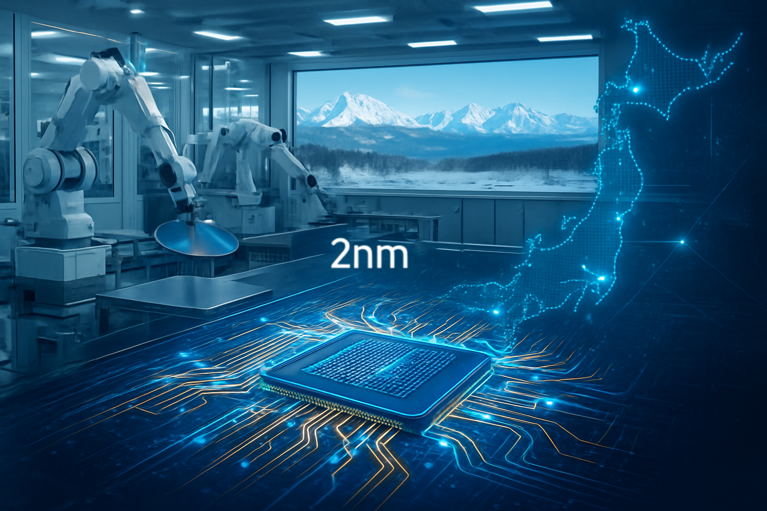
    In a decisive move to restore its status as a global technological powerhouse, the Japanese government has finalized a massive $6 billion (approximately 920 billion yen) investment into its home-grown semiconductor and AI ecosystem. This capital injection, spearheaded by the Ministry of Economy, Trade and Industry (METI), serves as the primary engine for Rapidus, a bold national venture aiming to leapfrog current manufacturing constraints and establish a domestic 2-nanometer (2nm) logic chip production line by 2027.

    The announcement marks a critical turning point for Japan, which once dominated the global chip market in the 1980s before losing ground to rivals in Taiwan and South Korea. By funding the development of cutting-edge AI hardware and advanced lithography, Japan is not merely seeking to participate in the current tech boom; it is positioning itself as a vital, independent pillar in the global supply chain, ensuring that the next generation of artificial intelligence is powered by Japanese-made silicon.

    Technical Leap: The 2nm GAA Frontier

    At the heart of this initiative is the Rapidus manufacturing facility in Chitose, Hokkaido, known as IIM-1. Unlike traditional foundries that have evolved incrementally, Rapidus is attempting a "generational leap" by moving directly into 2nm production using Gate-All-Around (GAA) transistor architecture. This technology is a significant departure from the FinFET (Fin Field-Effect Transistor) designs used in current 3nm and 5nm chips. GAA provides superior electrostatic control, significantly reducing power consumption while increasing processing speeds—a critical requirement for the massive computational demands of generative AI and autonomous systems.

    Technical execution is being bolstered by a "Triangle of Innovation" involving International Business Machines (NYSE: IBM), the European research hub imec, and Japan’s own Leading-edge Semiconductor Technology Center (LSTC). As of early 2026, Japanese engineers have completed intensive training at IBM’s Albany NanoTech Complex, and the IIM-1 facility has successfully demonstrated the operation of its first 2nm GAA prototype transistors. This collaboration allows Japan to bypass years of trial-and-error by licensing IBM’s foundational 2nm logic technology while utilizing imec’s expertise in Extreme Ultraviolet (EUV) lithography to achieve the precision required for such dense circuitry.

    Industry experts have reacted with a mixture of awe and skepticism, noting that while the technical roadmap is sound, the timeline is incredibly aggressive. Rapidus is essentially attempting to compress a decade of semiconductor evolution into less than five years. However, the integration of the LSTC as an R&D umbrella ensures that the project isn't just about manufacturing; it is also about designing the "Beyond 2nm" future, including advanced chiplet packaging and low-latency edge AI accelerators that could redefine how AI is deployed at the hardware level.

    Industry Impact: A New Power Dynamic

    The ripple effects of this $6 billion investment are being felt across the Tokyo Stock Exchange and Wall Street alike. SoftBank Group Corp. (TOKYO: 9984) has emerged as a primary beneficiary and advocate, viewing the domestic 2nm capability as essential for its vision of an AI-centric future. Similarly, Sony Group Corp. (NYSE: SONY) and Toyota Motor Corp. (NYSE: TM) are deeply integrated into the Rapidus consortium. For Sony, local 2nm production offers a pathway to more sophisticated AI-driven image sensors, while Toyota and its partner Denso Corp. (TOKYO: 6902) view the venture as a safeguard for the future of "Software Defined Vehicles" (SDVs) and autonomous driving.

    From a competitive standpoint, the emergence of Rapidus introduces a new dynamic for Taiwan Semiconductor Manufacturing Company (NYSE: TSM) and Intel Corp. (NASDAQ: INTC). While TSMC remains the undisputed leader in volume, Japan’s focus on a "high-mix, low-volume" specialized foundry model offers a strategic alternative for companies seeking to diversify their supply chains away from geopolitical flashpoints. This "Sovereign AI" strategy allows Japanese firms to develop proprietary AI chips without relying on foreign foundries, potentially disrupting the current market dominance held by major international players.

    Furthermore, the investment has catalyzed a private-sector surge. A consortium led by Mitsubishi UFJ Financial Group (NYSE: MUFG) has moved to provide trillions of yen in additional debt guarantees and loans, signaling that the financial industry views the semiconductor revival as a viable long-term bet. This public-private synergy provides Japan with a strategic advantage that few other nations can match: a unified industrial policy where the government, the banks, and the tech giants are all pulling in the same direction.

    Wider Significance: Geopolitical Resilience and AI Sovereignty

    Beyond the technical specifications, Japan’s $6 billion investment is a masterstroke of geopolitical positioning. In an era defined by the "chip wars" between the U.S. and China, Japan is carving out a role as a stable, high-tech sanctuary. By building the "Hokkaido Silicon Valley," the Japanese government is creating a self-sustaining ecosystem that attracts global suppliers of materials and equipment, such as Tokyo Electron and Shin-Etsu Chemical. This reduces the risk of supply chain shocks and ensures that Japan remains indispensable to the global economy.

    The broader AI landscape is currently grappling with a "compute crunch," where the demand for high-performance chips far outstrips supply. Japan’s entry into the 2nm space is a direct response to this trend. If successful, it will provide a much-needed release valve for the industry, offering a new source of the ultra-efficient chips required for the next wave of large language models (LLMs) and robotic process automation. It represents a shift from "AI software" dominance to "AI hardware" sovereignty, a move that mirrors previous milestones like the development of the first integrated circuits.

    However, the path is not without concerns. Critics point to the immense cost of maintaining EUV lithography machines and the potential for a talent shortage. To combat this, the LSTC has launched "Silicon Talent" initiatives across 15 universities, attempting to train a new generation of semiconductor engineers. The success of this human capital investment will be just as critical as the financial one, as the complexity of 2nm manufacturing requires a level of precision that leaves zero room for error.

    Future Developments: The Road to 1.4nm

    Looking ahead, the next 18 months will be the most critical in Japan’s technological history. The immediate goal is the launch of an advanced packaging pilot line at the Rapidus Chiplet Solutions center in April 2026. This facility will focus on "chiplets"—a method of stacking different types of processors together—which is widely considered the future of AI hardware design. By late 2026, the industry expects to see the first full-wafer runs from the Chitose plant, serving as a "litmus test" for the 2027 mass production deadline.

    In the long term, Japan is already looking past the 2nm horizon. Plans are reportedly in development for a second Hokkaido facility dedicated to 1.4nm production, with construction potentially beginning as early as 2027. Experts predict that if Japan can hit its 2nm targets, it will trigger a massive influx of global AI startups moving their hardware development to Japanese soil, drawn by the combination of cutting-edge manufacturing and a stable political environment.

    Closing Thoughts: A Historic Rebound

    Japan’s $6 billion investment is more than just a financial commitment; it is a declaration of intent. By backing Rapidus and the LSTC, the nation is betting that it can reclaim its role as the world’s premier high-tech workshop. The strategy is clear: secure the technology through global partnerships, fund the infrastructure with state capital, and drive the demand through a consortium of national champions like Toyota and Sony.

    The significance of this development in AI history cannot be overstated. We are witnessing the birth of a decentralized semiconductor map, where the ability to produce the world’s most advanced chips is no longer concentrated in just one or two regions. As we move toward the 2027 production goal, the world will be watching Hokkaido. The success of Rapidus would not only be a victory for Japan but a stabilizing force for the global AI industry, ensuring that the hardware of the future is as diverse and resilient as the software it supports.


    This content is intended for informational purposes only and represents analysis of current AI developments.

    TokenRing AI delivers enterprise-grade solutions for multi-agent AI workflow orchestration, AI-powered development tools, and seamless remote collaboration platforms.
    For more information, visit https://www.tokenring.ai/.
  • Backside Power Delivery: The Secret Weapon for Sub-2nm Chip Efficiency

    Backside Power Delivery: The Secret Weapon for Sub-2nm Chip Efficiency

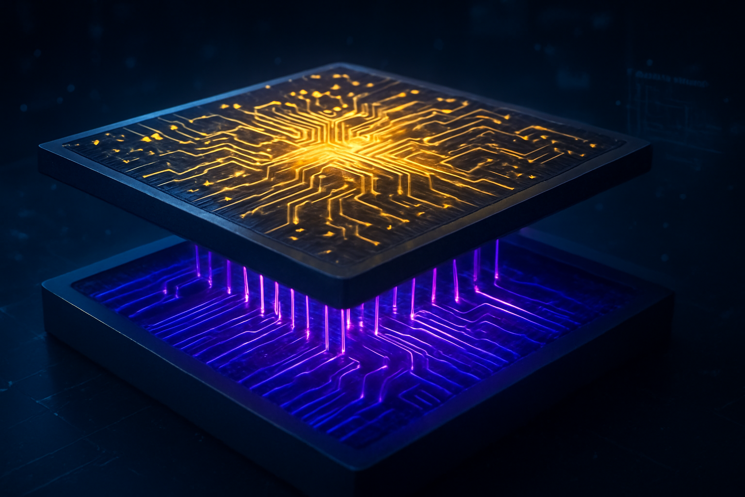
    As the artificial intelligence revolution enters its most demanding phase in 2026, the semiconductor industry has reached a pivotal turning point. The traditional methods of powering microchips—which have remained largely unchanged for decades—are being discarded in favor of a radical new architecture known as Backside Power Delivery (BSPDN). This shift is not merely an incremental upgrade; it is a fundamental redesign of the silicon wafer that is proving to be the "secret weapon" for the next generation of sub-2nm AI processors.

    By moving the complex network of power delivery lines from the top of the silicon wafer to its underside, chipmakers are finally breaking the "power wall" that has threatened to stall Moore’s Law. This innovation, spearheaded by industry giants Intel and TSMC, allows for significantly higher power efficiency, reduced signal interference, and a dramatic increase in logic density. For the AI industry, which is currently grappling with the immense energy demands of trillion-parameter models, BSPDN is the critical infrastructure enabling the hardware of tomorrow.

    The Great Flip: Moving Power to the Backside

    The technical transition to Backside Power Delivery represents the most significant architectural change in chip manufacturing since the introduction of FinFET transistors. Historically, both power and data signals were routed through a dense "forest" of metal layers on the front side of the wafer. As transistors shrank to the 2nm level and below, this "Front-side Power Delivery" (FSPDN) became a major bottleneck. The power lines and signal lines competed for the same limited space, leading to "IR drop"—a phenomenon where voltage is lost to resistance before it even reaches the transistors—and signal interference that hampered performance.

    Intel Corporation (NASDAQ: INTC) was the first to cross the finish line with its implementation, branded as PowerVia. Integrated into the Intel 18A (1.8nm) node, PowerVia utilizes Nano-Through Silicon Vias (nTSVs) to deliver electricity directly to the transistors from the back. This approach has already demonstrated a 30% reduction in IR droop and a roughly 6% increase in frequency at iso-power. Meanwhile, Taiwan Semiconductor Manufacturing Co. (NYSE: TSM) is preparing its Super Power Rail technology for the A16 node. Unlike Intel’s nTSVs, TSMC’s implementation uses direct contact to the source and drain, which is more complex to manufacture but promises an 8–10% speed improvement and up to 20% power reduction compared to its previous N2P node.

    The reaction from the AI research and hardware communities has been overwhelmingly positive. Experts note that while previous node transitions focused on making transistors smaller, BSPDN focuses on making them more accessible. By clearing the "congestion" on the front side of the chip, designers can now pack more logic gates and High Bandwidth Memory (HBM) interconnects into the same physical area. This "unclogging" of the chip's architecture is what allows for the extreme density required by the latest AI accelerators.

    A New Competitive Landscape for AI Giants

    The arrival of BSPDN has sparked a strategic reshuffling among the world’s most valuable tech companies. Intel’s early success with PowerVia has allowed it to secure major foundry customers who were previously exclusive to TSMC. Microsoft (NASDAQ: MSFT), for instance, has become a lead customer for Intel’s 18A process, utilizing it for its Maia 3 AI accelerators. For Microsoft, the power efficiency gains of BSPDN are vital for managing the astronomical electricity costs of its global data center footprint.

    TSMC, however, remains the dominant force in the high-end AI market. While its A16 node is not scheduled for high-volume manufacturing until the second half of 2026, NVIDIA (NASDAQ: NVDA) has reportedly secured early access for its upcoming "Feynman" architecture. NVIDIA’s current Blackwell successors already push the limits of thermal design power (TDP), often exceeding 1,000 watts. The Super Power Rail technology in A16 is seen as the only viable path to sustaining the performance leaps NVIDIA needs for its 2027 and 2028 roadmaps.

    Even Apple (NASDAQ: AAPL), which has long been TSMC’s most loyal partner, is reportedly exploring diversification. While Apple is expected to use TSMC’s N2P for the iPhone 18 Pro in late 2026, rumors suggest the company is qualifying Intel’s 18A for its entry-level M-series chips in 2027. This shift highlights how critical BSPDN has become; the competitive advantage is no longer just about who has the smallest transistors, but who can power them most efficiently.

    Breaking the Power Wall and Enabling 3D Silicon

    The broader significance of Backside Power Delivery lies in its ability to solve the thermal and energy crises currently facing the AI landscape. As AI models grow, the chips that train them require more current. In a traditional design, the heat generated by power delivery on the front side of the chip sits directly on top of the heat-generating transistors, creating a "thermal sandwich" that is difficult to cool. By moving power to the backside, the front of the chip can be more effectively cooled by direct-contact liquid cooling or advanced heat sinks.

    This architectural shift also paves the way for advanced 3D-stacked chips. In a 3D configuration, multiple layers of logic and memory are piled on top of each other. Previously, getting power to the middle layers of such a stack was a logistical nightmare. BSPDN provides a blueprint for "sandwiching" power and cooling between logic layers, which many believe is the only way to eventually achieve "brain-scale" computing.

    However, the transition is not without its concerns. The manufacturing process for BSPDN requires extreme wafer thinning—grinding the silicon down to just a few micrometers—and complex wafer-to-wafer bonding. This increases the risk of manufacturing defects and could lead to higher initial costs for AI startups. There is also the concern of "vendor lock-in," as the design tools required for Intel’s PowerVia and TSMC’s Super Power Rail are not fully interchangeable, forcing chip designers to choose a side early in the development cycle.

    The Road to 1nm and Beyond

    Looking ahead, the successful deployment of BSPDN in 2026 is just the beginning. Experts predict that by 2028, backside power will be standard across all high-performance computing (HPC) and mobile chips. The next frontier will be the integration of optical interconnects directly onto the backside of the wafer, allowing chips to communicate via light rather than electricity, further reducing heat and increasing bandwidth.

    In the near term, the industry is watching the H2 2026 ramp-up of TSMC’s A16 node. If TSMC can achieve high yields quickly, it could accelerate the release of OpenAI’s rumored custom "XPU" (eXtreme Processing Unit), which is being designed in collaboration with Broadcom (NASDAQ: AVGO) to leverage Super Power Rail for GPT-6 training clusters. The challenge remains the sheer complexity of the manufacturing process, but the rewards—chips that are 20% faster and significantly cooler—are too great for any major player to ignore.

    A Milestone in Semiconductor History

    Backside Power Delivery marks the end of the "two-dimensional" era of chip design and the beginning of a truly three-dimensional future. By decoupling the delivery of energy from the processing of data, Intel and TSMC have provided the AI industry with a new lease on life. This development will likely be remembered as the moment when the physical limits of silicon were pushed back, allowing the exponential growth of artificial intelligence to continue unabated.

    As we move through 2026, the key metrics to watch will be the production yields of TSMC’s A16 and the real-world performance of Intel’s 18A-based server chips. For the first time in years, the "how" of chip manufacturing is just as important as the "how small." The secret weapon for sub-2nm efficiency is no longer a secret—it is the new foundation of the digital world.


    This content is intended for informational purposes only and represents analysis of current AI developments.

    TokenRing AI delivers enterprise-grade solutions for multi-agent AI workflow orchestration, AI-powered development tools, and seamless remote collaboration platforms.
    For more information, visit https://www.tokenring.ai/.

  • The 2-Nanometer Frontier: A Global Race to Reshape AI and Computing

    The 2-Nanometer Frontier: A Global Race to Reshape AI and Computing

    The semiconductor industry is currently embroiled in an intense global race to develop and mass-produce advanced 2-nanometer (nm) chips, pushing the very boundaries of miniaturization and performance. This pursuit represents a pivotal moment for technology, promising unprecedented advancements that will redefine computing capabilities across nearly every sector. These next-generation chips are poised to deliver revolutionary improvements in processing speed and energy efficiency, allowing for significantly more powerful and compact devices.

    The immediate significance of 2nm chips is profound. Prototypes, such as IBM's groundbreaking 2nm chip, project an astonishing 45% higher performance or 75% lower energy consumption compared to current 7nm chips. Similarly, Taiwan Semiconductor Manufacturing Company (TSMC) (NYSE: TSM) aims for a 10-15% performance boost and a 25-30% reduction in power consumption over its 3nm predecessors. This leap in efficiency and power directly translates to longer battery life for mobile devices, faster processing for AI workloads, and a reduced carbon footprint for data centers. Moreover, the smaller 2nm process allows for an exponential increase in transistor density, with designs like IBM's capable of fitting up to 50 billion transistors on a chip the size of a fingernail, ensuring the continued march of Moore's Law. This miniaturization is crucial for accelerating advancements in artificial intelligence (AI), high-performance computing (HPC), autonomous vehicles, 5G/6G communication, and the Internet of Things (IoT).

    The Technical Leap: Gate-All-Around and Beyond

    The transition to 2nm technology is fundamentally driven by a significant architectural shift in transistor design. For years, the industry relied on FinFET (Fin Field-Effect Transistor) architecture, but at 2nm and beyond, FinFETs face physical limitations in controlling current leakage and maintaining performance. The key technological advancement enabling 2nm is the widespread adoption of Gate-All-Around (GAA) transistor architecture, often implemented as nanosheet or nanowire FETs. This innovative design allows the gate to completely surround the channel, providing superior electrostatic control, which significantly reduces leakage current and enhances performance at smaller scales.

    Leading the charge in this technical evolution are industry giants like TSMC, Samsung (KRX: 005930), and Intel (NASDAQ: INTC). TSMC's N2 process, set for mass production in the second half of 2025, is its first to fully embrace GAA. Samsung, a fierce competitor, was an early adopter of GAA for its 3nm chips and is "all-in" on the technology for its 2nm process, slated for production in 2025. Intel, with its aggressive 18A (1.8nm-class) process, incorporates its own version of GAAFETs, dubbed RibbonFET, alongside a novel power delivery system called PowerVia, which moves power lines to the backside of the wafer to free up space on the front for more signal routing. These innovations are critical for achieving the density and performance targets of the 2nm node.

    The technical specifications of these 2nm chips are staggering. Beyond raw performance and power efficiency gains, the increased transistor density allows for more complex and specialized logic circuits to be integrated directly onto the chip. This is particularly beneficial for AI accelerators, enabling more sophisticated neural network architectures and on-device AI processing. Initial reactions from the AI research community and industry experts have been overwhelmingly positive, marked by intense demand. TSMC has reported promising early yields for its N2 process, estimated between 60% and 70%, and its 2nm production capacity for 2026 is already fully booked, with Apple (NASDAQ: AAPL) reportedly reserving over half of the initial output for its future iPhones and Macs. This high demand underscores the industry's belief that 2nm chips are not just an incremental upgrade, but a foundational technology for the next wave of innovation, especially in AI. The economic and geopolitical importance of mastering this technology cannot be overstated, as nations invest heavily to secure domestic semiconductor production capabilities.

    Competitive Implications and Market Disruption

    The global race for 2-nanometer chips is creating a highly competitive landscape, with significant implications for AI companies, tech giants, and startups alike. The foundries that successfully achieve high-volume, high-yield 2nm production stand to gain immense strategic advantages, dictating the pace of innovation for their customers. TSMC, with its reported superior early yields and fully booked 2nm capacity for 2026, appears to be in a commanding position, solidifying its role as the primary enabler for many of the world's leading AI and tech companies. Companies like Apple, AMD (NASDAQ: AMD), NVIDIA (NASDAQ: NVDA), and Qualcomm (NASDAQ: QCOM) are deeply reliant on these advanced nodes for their next-generation products, making access to TSMC's 2nm capacity a critical competitive differentiator.

    Samsung is aggressively pursuing its 2nm roadmap, aiming to catch up and even surpass TSMC. Its "all-in" strategy on GAA technology and significant deals, such as the reported $16.5 billion agreement with Tesla (NASDAQ: TSLA) for 2nm chips, indicate its determination to secure a substantial share of the high-end foundry market. If Samsung can consistently improve its yield rates, it could offer a crucial alternative sourcing option for companies looking to diversify their supply chains or gain a competitive edge. Intel, with its ambitious 18A process, is not only aiming to reclaim its manufacturing leadership but also to become a major foundry for external customers. Its recent announcement of mass production for 18A chips in October 2025, claiming to be ahead of some competitors in this class, signals a serious intent to disrupt the foundry market. The success of Intel Foundry Services (IFS) in attracting major clients will be a key factor in its resurgence.

    The availability of 2nm chips will profoundly disrupt existing products and services. For AI, the enhanced performance and efficiency mean that more complex models can run faster, both in data centers and on edge devices. This could lead to a new generation of AI-powered applications that were previously computationally infeasible. Startups focusing on advanced AI hardware or highly optimized AI software stand to benefit immensely, as they can leverage these powerful new chips to bring their innovative solutions to market. However, companies reliant on older process nodes may find their products quickly becoming obsolete, facing pressure to adopt the latest technology or risk falling behind. The immense cost of 2nm chip development and production also means that only the largest and most well-funded companies can afford to design and utilize these cutting-edge components, potentially widening the gap between tech giants and smaller players, unless innovative ways to access these technologies emerge.

    Wider Significance in the AI Landscape

    The advent of 2-nanometer chips represents a monumental stride that will profoundly reshape the broader AI landscape and accelerate prevailing technological trends. At its core, this miniaturization and performance boost directly fuels the insatiable demand for computational power required by increasingly complex AI models, particularly in areas like large language models (LLMs), generative AI, and advanced machine learning. These chips will enable faster training of models, more efficient inference at scale, and the proliferation of on-device AI capabilities, moving intelligence closer to the data source and reducing latency. This fits perfectly into the trend of pervasive AI, where AI is integrated into every aspect of computing, from cloud servers to personal devices.

    The impacts of 2nm chips are far-reaching. In AI, they will unlock new levels of performance for real-time processing in autonomous systems, enhance the capabilities of AI-driven scientific discovery, and make advanced AI more accessible and energy-efficient for a wider array of applications. For instance, the ability to run sophisticated AI algorithms directly on a smartphone or in an autonomous vehicle without constant cloud connectivity opens up new paradigms for privacy, security, and responsiveness. Potential concerns, however, include the escalating cost of developing and manufacturing these cutting-edge chips, which could further centralize power among a few dominant foundries and chip designers. There are also environmental considerations regarding the energy consumption of fabrication plants and the lifecycle of these increasingly complex devices.

    Comparing this milestone to previous AI breakthroughs, the 2nm chip race is analogous to the foundational leaps in transistor technology that enabled the personal computer revolution or the rise of the internet. Just as those advancements provided the hardware bedrock for subsequent software innovations, 2nm chips will serve as the crucial infrastructure for the next generation of AI. They promise to move AI beyond its current capabilities, allowing for more human-like reasoning, more robust decision-making in real-world scenarios, and the development of truly intelligent agents. This is not merely an incremental improvement but a foundational shift that will underpin the next decade of AI progress, facilitating advancements in areas from personalized medicine to climate modeling.

    The Road Ahead: Future Developments and Challenges

    The immediate future will see the ramp-up of 2nm mass production from TSMC, Samsung, and Intel throughout 2025 and into 2026. Experts predict a fierce battle for market share, with each foundry striving to optimize yields and secure long-term contracts with key customers. Near-term developments will focus on integrating these chips into flagship products: Apple's next-generation iPhones and Macs, new high-performance computing platforms from AMD and NVIDIA, and advanced mobile processors from Qualcomm and MediaTek. The initial applications will primarily target high-end consumer electronics, data center AI accelerators, and specialized components for autonomous driving and advanced networking.

    Looking further ahead, the pursuit of even smaller nodes, such as 1.4nm (often referred to as A14) and potentially 1nm, is already underway. Challenges that need to be addressed include the increasing complexity and cost of manufacturing, which demands ever more sophisticated Extreme Ultraviolet (EUV) lithography machines and advanced materials science. The physical limits of silicon-based transistors are also becoming apparent, prompting research into alternative materials and novel computing paradigms like quantum computing or neuromorphic chips. Experts predict that while silicon will remain dominant for the foreseeable future, hybrid approaches and new architectures will become increasingly important to continue the trajectory of performance improvements. The integration of specialized AI accelerators directly onto the chip, designed for specific AI workloads, will also become more prevalent.

    What experts predict will happen next is a continued specialization of chip design. Instead of a one-size-fits-all approach, we will see highly customized chips optimized for specific AI tasks, leveraging the increased transistor density of 2nm and beyond. This will lead to more efficient and powerful AI systems tailored for everything from edge inference in IoT devices to massive cloud-based training of foundation models. The geopolitical implications will also intensify, as nations recognize the strategic importance of domestic chip manufacturing capabilities, leading to further investments and potential trade policy shifts. The coming years will be defined by how successfully the industry navigates these technical, economic, and geopolitical challenges to fully harness the potential of 2nm technology.

    A New Era of Computing: Wrap-Up

    The global race to produce 2-nanometer chips marks a monumental inflection point in the history of technology, heralding a new era of unprecedented computing power and efficiency. The key takeaways from this intense competition are the critical shift to Gate-All-Around (GAA) transistor architecture, the staggering performance and power efficiency gains promised by these chips, and the fierce competition among TSMC, Samsung, and Intel to lead this technological frontier. These advancements are not merely incremental; they are foundational, providing the essential hardware bedrock for the next generation of artificial intelligence, high-performance computing, and ubiquitous smart devices.

    This development's significance in AI history cannot be overstated. Just as earlier chip advancements enabled the rise of deep learning, 2nm chips will unlock new paradigms for AI, allowing for more complex models, faster training, and pervasive on-device intelligence. They will accelerate the development of truly autonomous systems, more sophisticated generative AI, and AI-driven solutions across science, medicine, and industry. The long-term impact will be a world where AI is more deeply integrated, more powerful, and more energy-efficient, driving innovation across every sector.

    In the coming weeks and months, industry observers should watch for updates on yield rates from the major foundries, announcements of new design wins for 2nm processes, and the first wave of consumer and enterprise products incorporating these cutting-edge chips. The strategic positioning of Intel Foundry Services, the continued expansion plans of TSMC and Samsung, and the emergence of new players like Rapidus will also be crucial indicators of the future trajectory of the semiconductor industry. The 2nm frontier is not just about smaller chips; it's about building the fundamental infrastructure for a smarter, more connected, and more capable future powered by advanced AI.


    This content is intended for informational purposes only and represents analysis of current AI developments.

    TokenRing AI delivers enterprise-grade solutions for multi-agent AI workflow orchestration, AI-powered development tools, and seamless remote collaboration platforms.
    For more information, visit https://www.tokenring.ai/.
  • Japan’s Material Maestros: Fueling the 2nm Chip Revolution and AI’s Future

    Japan’s Material Maestros: Fueling the 2nm Chip Revolution and AI’s Future

    In a significant strategic pivot, Japan's semiconductor materials suppliers are dramatically ramping up capital expenditure, positioning themselves as indispensable architects in the global race to mass-produce advanced 2-nanometer (nm) chips. This surge in investment, coupled with robust government backing and industry collaboration, underscores Japan's renewed ambition to reclaim a pivotal role in the semiconductor supply chain, a move that carries profound implications for the future of artificial intelligence (AI) and the broader tech industry.

    The immediate significance of this development cannot be overstated. As the world grapples with persistent supply chain vulnerabilities and escalating geopolitical tensions, Japan's concentrated effort to dominate the foundational materials segment for next-generation chips offers a critical pathway towards greater global resilience. For AI developers and tech giants alike, the promise of 2nm chips—delivering unprecedented processing power and energy efficiency—is a game-changer, and Japan's material prowess is proving to be the silent engine driving this technological leap.

    The Microscopic Frontier: Japan's Advanced Materials Edge

    The journey to 2nm chip manufacturing is not merely about shrinking transistors; it demands an entirely new paradigm in material science and advanced packaging. Japanese companies are at the forefront of this microscopic frontier, investing heavily in specialized materials crucial for processes like 3D chip packaging, which is essential for achieving the density and performance required at 2nm. This includes the development of sophisticated temporary bonding adhesives, advanced resins compatible with complex back-end production, and precision equipment for removing microscopic debris that can compromise chip integrity. The alliance JOINT2 (Jisso Open Innovation Network of Tops 2), a consortium of Japanese firms including Renosac and Ajinomoto Fine-Techno, is actively collaborating with the government-backed Rapidus and the Leading-Edge Semiconductor Technology Center (LSTC) on these advanced packaging technologies.

    These advancements represent a significant departure from previous manufacturing approaches, where the focus was primarily on lithography and front-end processes. At 2nm, the intricate interplay of materials, their purity, and how they interact during advanced packaging, including Gate-All-Around (GAA) transistors, becomes paramount. GAA transistors, which surround the gate on all four sides of the channel, are a key innovation for 2nm, offering superior gate control and reduced leakage compared to FinFETs used in previous nodes. This technical shift necessitates materials with unparalleled precision and consistency. Initial reactions from the AI research community and industry experts highlight the strategic brilliance of Japan's focus on materials and equipment, recognizing it as a pragmatic and high-impact approach to re-enter the leading edge of chip manufacturing.

    The performance gains promised by 2nm chips are staggering: up to 45% faster or 75% lower power consumption compared to 3nm chips. Achieving these metrics relies heavily on the quality and innovation of the underlying materials. Japanese giants like SUMCO (TYO: 3436) and Shin-Etsu Chemical (TYO: 4063) already command approximately 60% of the global silicon wafer market, and their continued investment ensures a robust supply of foundational elements. Other key players like Nissan Chemical (TYO: 4021), Showa Denko (TYO: 4004), and Sumitomo Bakelite (TYO: 4203) are scaling up investments in everything from temporary bonding adhesives to specialized resins, cementing Japan's role as the indispensable material supplier for the next generation of semiconductors.

    Reshaping the AI Landscape: Beneficiaries and Competitive Shifts

    The implications of Japan's burgeoning role in 2nm chip materials ripple across the global technology ecosystem, profoundly affecting AI companies, tech giants, and nascent startups. Global chipmakers such as Taiwan Semiconductor Manufacturing Company (TSMC) (TPE: 2330), Samsung Electronics (KRX: 005930), and Intel (NASDAQ: INTC), all vying for 2nm production leadership, will heavily rely on the advanced materials and equipment supplied by Japanese firms. This dependency ensures that Japan's material suppliers are not merely participants but critical enablers of the next wave of computing power.

    Within Japan, the government-backed Rapidus consortium, comprising heavyweights like Denso (TYO: 6902), Kioxia, MUFG Bank (TYO: 8306), NEC (TYO: 6701), NTT (TYO: 9432), SoftBank (TYO: 9984), Sony (TYO: 6758), and Toyota (TYO: 7203), stands to be a primary beneficiary. Their collective investment in Rapidus aims to establish domestic 2nm chip manufacturing by 2027, securing a strategic advantage for Japanese industries in AI, automotive, and high-performance computing. This initiative directly addresses competitive concerns, aiming to prevent Japanese equipment and materials manufacturers from relocating overseas and consolidating the nation's technological base.

    The competitive landscape is set for a significant shift. Japan's strategic focus on the high-value, high-barrier-to-entry materials segment diversifies the global semiconductor supply chain, reducing over-reliance on a few key regions for advanced chip manufacturing. This move could potentially disrupt existing product development cycles by enabling more powerful and energy-efficient AI hardware, fostering innovation in areas like edge AI, autonomous systems, and advanced robotics. For startups developing AI solutions, access to these cutting-edge chips means the ability to run more complex models locally, opening up new product categories and services that were previously computationally unfeasible.

    Wider Significance: A Pillar for Global Tech Sovereignty

    Japan's resurgence in semiconductor materials for 2nm chips extends far beyond mere commercial interests; it is a critical component of the broader global AI landscape and a strategic move towards technological sovereignty. These ultra-advanced chips are the foundational bedrock for the next generation of AI, enabling unprecedented capabilities in large language models, complex simulations, and real-time data processing. They are also indispensable for the development of 6G wireless communication, fully autonomous driving systems, and the nascent field of quantum computing.

    The impacts of this initiative are multi-faceted. On a geopolitical level, it enhances global supply chain resilience by diversifying the sources of critical semiconductor components, a lesson painfully learned during recent global shortages. Economically, it represents a massive investment in Japan's high-tech manufacturing base, promising job creation, innovation, and sustained growth. From a national security perspective, securing domestic access to leading-edge chip technology is paramount for maintaining a competitive edge in defense, intelligence, and critical infrastructure.

    However, potential concerns also loom. The sheer scale of investment required, coupled with intense global competition from established chip manufacturing giants, presents significant challenges. Talent acquisition and retention in a highly specialized field will also be crucial. Nevertheless, this effort marks a determined attempt by Japan to regain leadership in an industry it once dominated in the 1980s. Unlike previous attempts, the current strategy focuses on leveraging existing strengths in materials and equipment, rather than attempting to compete directly with foundry giants on all fronts, making it a more focused and potentially more successful endeavor.

    The Road Ahead: Anticipating Next-Gen AI Enablers

    Looking ahead, the near-term developments are poised to be rapid and transformative. Rapidus, with substantial government backing (including an additional 100 billion yen under the fiscal 2025 budget), is on an aggressive timeline. Test production at its Innovative Integration for Manufacturing (IIM-1) facility in Chitose, Hokkaido, is slated to commence in April 2025. The company has already successfully prototyped Japan's first 2nm wafer in August 2025, a significant milestone. Global competitors like TSMC aim for 2nm mass production in the second half of 2025, while Samsung targets 2025, and Intel's (NASDAQ: INTC) 18A (2nm equivalent) is projected for late 2024. These timelines underscore the fierce competition but also the rapid progression towards the 2nm era.

    In the long term, the applications and use cases on the horizon are revolutionary. More powerful and energy-efficient 2nm chips will unlock capabilities for AI models that are currently constrained by computational limits, leading to breakthroughs in fields like personalized medicine, climate modeling, and advanced robotics. Edge AI devices will become significantly more intelligent and autonomous, processing complex data locally without constant cloud connectivity. The challenges, however, remain substantial, particularly in achieving high yield rates, managing the escalating costs of advanced manufacturing, and sustaining continuous research and development to push beyond 2nm to even smaller nodes.

    Experts predict that Japan's strategic focus on materials and equipment will solidify its position as an indispensable partner in the global semiconductor ecosystem. This specialized approach, coupled with strong government-industry collaboration, is expected to lead to further innovations in material science, potentially enabling future breakthroughs in chip architecture and packaging beyond 2nm. The ongoing success of Rapidus and its Japanese material suppliers will be a critical indicator of this trajectory.

    A New Era of Japanese Leadership in Advanced Computing

    In summary, Japan's semiconductor materials suppliers are unequivocally stepping into a critical leadership role in the production of advanced 2-nanometer chips. This strategic resurgence, driven by significant capital investment, robust government support for initiatives like Rapidus, and a deep-seated expertise in material science, is not merely a commercial endeavor but a national imperative. It represents a crucial step towards building a more resilient and diversified global semiconductor supply chain, essential for the continued progress of artificial intelligence and other cutting-edge technologies.

    This development marks a significant chapter in AI history, as the availability of 2nm chips will fundamentally reshape the capabilities of AI systems, enabling more powerful, efficient, and intelligent applications across every sector. The long-term impact will likely see Japan re-established as a technological powerhouse, not through direct competition in chip fabrication across all nodes, but by dominating the foundational elements that make advanced manufacturing possible. What to watch for in the coming weeks and months includes Rapidus's progress towards its 2025 test production goals, further announcements regarding material innovation from key Japanese suppliers, and the broader global competition for 2nm chip supremacy. The stage is set for a new era where Japan's mastery of materials will power the AI revolution.


    This content is intended for informational purposes only and represents analysis of current AI developments.

    TokenRing AI delivers enterprise-grade solutions for multi-agent AI workflow orchestration, AI-powered development tools, and seamless remote collaboration platforms.
    For more information, visit https://www.tokenring.ai/.