As of February 6, 2026, the global semiconductor landscape has reached a fever pitch, with Taiwan Semiconductor Manufacturing Company (NYSE: TSM) standing at the absolute center of the storm. In its most recent quarterly report, the foundry giant posted financial results that shattered analyst expectations, driven by an insatiable hunger for high-performance computing (HPC) and artificial intelligence hardware. With net income soaring 35% year-over-year to approximately $16 billion, TSMC has confirmed that the AI revolution is not just a passing phase, but a structural shift in the global economy.
The most significant takeaway from the announcement is the company’s accelerated roadmap toward the A16 (1.6nm) node. As the world transitions from the current 3nm standard to the upcoming 2nm production line, TSMC’s vision for 1.6nm silicon represents a technological frontier that promises to redefine the limits of computational density. With the company’s AI segment now projected to sustain a mid-to-high 50% compound annual growth rate (CAGR) through the end of the decade, the race for "Angstrom-era" dominance has officially begun.
The Technical Frontier: From N2 Nanosheets to A16 Super Power Rails
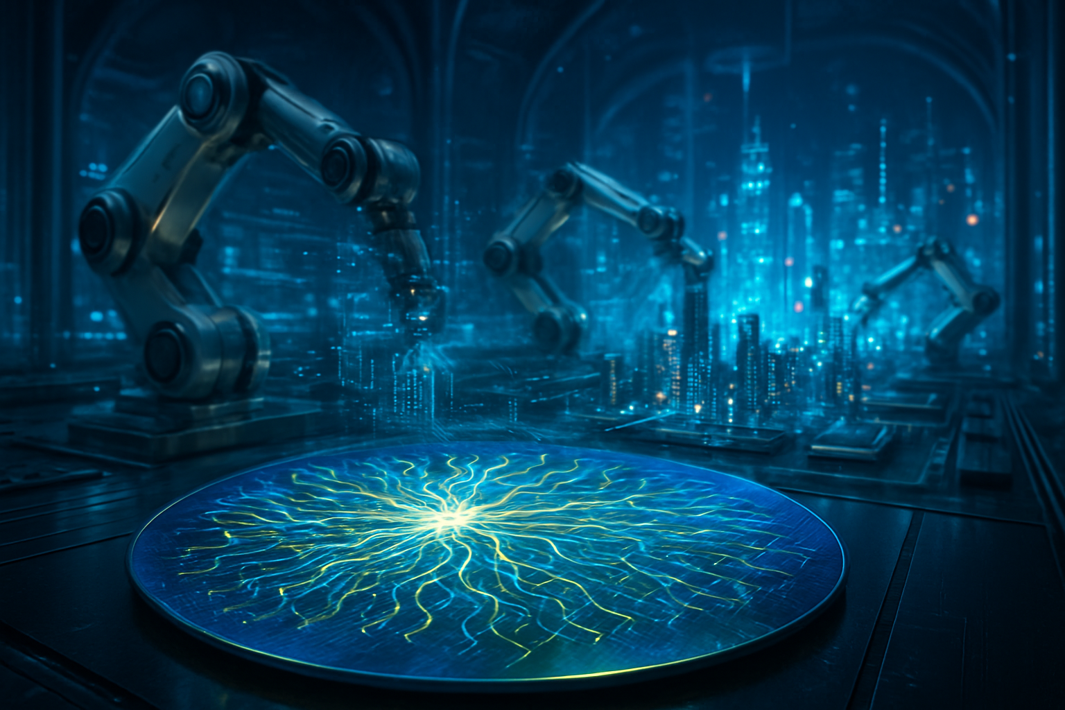
The shift to the 2nm (N2) node, which entered high-volume manufacturing in late 2025 and is reaching consumer devices in early 2026, marks TSMC’s historic departure from the long-standing FinFET transistor architecture. N2 utilizes Gate-All-Around (GAA) nanosheet transistors, which allow for finer control over current flow, drastically reducing power leakage while increasing switching speeds. Compared to the N3E process, N2 offers a 10% to 15% speed improvement at the same power, or a 25% to 30% power reduction at the same speed. This leap is critical for the next generation of mobile processors and AI accelerators that must balance extreme performance with thermal constraints.
However, the real "AI game-changer" is the A16 node, scheduled for volume production in the second half of 2026. The A16 process introduces a revolutionary feature known as the "Super Power Rail" (SPR)—TSMC’s proprietary implementation of backside power delivery. By moving the power distribution network from the front of the wafer to the back, TSMC eliminates the competition for space between signal wires and power lines. This design reduces the "IR drop" (voltage loss), enabling chips to run at higher frequencies and allowing for significantly higher transistor density.
Industry experts and the AI research community have hailed the A16 announcement as the most significant architectural shift since the introduction of FinFET. By decoupling the power and signal layers, TSMC is providing a path for AI chip designers to build massive, monolithic dies that can handle the quadrillions of parameters required by 2026-era Large Language Models (LLMs). This technology specifically targets the "memory wall" and power delivery bottlenecks that have begun to plague current-generation AI hardware.
Market Impact: The Scramble for Advanced Silicon
The financial implications of TSMC’s roadmap are profound, particularly for the industry's heaviest hitters. NVIDIA (NASDAQ: NVDA) is widely reported to be the lead customer for the A16 node, with plans to utilize the technology for its upcoming "Feynman" architecture. By securing early access to A16, NVIDIA maintains its strategic advantage over rivals, ensuring that its AI accelerators remain the gold standard for data center training. Similarly, Apple (NASDAQ: AAPL) remains a cornerstone partner, having already transitioned its latest flagship devices to the N2 node, further distancing itself from competitors in the premium smartphone market.
The competitive landscape is also shifting for "Hyperscalers" like Microsoft (NASDAQ: MSFT), Alphabet (NASDAQ: GOOGL), and Meta (NASDAQ: META). In a notable trend throughout 2025 and into 2026, these cloud giants have begun bypassing traditional chip designers to work directly with TSMC on custom silicon. By designing their own ASICs (Application-Specific Integrated Circuits) on the N2 and A16 nodes, these companies can optimize hardware specifically for their internal AI workloads, potentially disrupting the market for general-purpose GPUs.
This surge in demand has granted TSMC unprecedented pricing power. With a market share in the advanced foundry space hovering around 72%, TSMC has successfully implemented annual price increases through 2029. For startups and smaller AI labs, this creates a high barrier to entry; the cost of designing and manufacturing a chip on a sub-2nm node is estimated to exceed $1 billion when accounting for R&D and tape-out fees. This concentration of power effectively makes TSMC the "gatekeeper" of the AI era, where access to 2nm and 1.6nm capacity is as valuable as the AI algorithms themselves.
The Broader AI Landscape: Silicon as the New Oil
TSMC’s performance serves as a barometer for the wider AI landscape, which has evolved from speculative software to heavy physical infrastructure. The mid-to-high 50% CAGR in the company's AI segment confirms that the "silicon bottleneck" remains the primary constraint on global AI progress. While software efficiency has improved, the demand for raw compute continues to scale exponentially. We are now in an era where the geostrategic importance of a single company—TSMC—parallels that of major oil-producing nations in the 20th century.
However, this rapid advancement is not without concerns. The immense capital expenditure required to build and maintain 2nm and 1.6nm fabs—with TSMC's 2026 CapEx projected at a staggering $52 billion to $56 billion—raises questions about the sustainability of the AI investment cycle. Critics point to the potential for a "capacity bubble" if AI monetization does not keep pace with the cost of the underlying hardware. Furthermore, the environmental impact of these high-power fabs and the energy required to run the AI chips they produce are becoming central themes in regulatory discussions.
Comparatively, the transition to A16 is being viewed as a milestone on par with the 7nm breakthrough in 2018. Just as 7nm enabled the modern smartphone and cloud era, A16 is expected to enable "Everywhere AI"—the integration of sophisticated, locally-running AI models into everything from autonomous vehicles to industrial robotics. The move to backside power delivery is more than a technical refinement; it is a fundamental reconfiguration of the semiconductor to meet the specific electrical demands of neural network processing.
Future Outlook: The Road to 1nm and Beyond
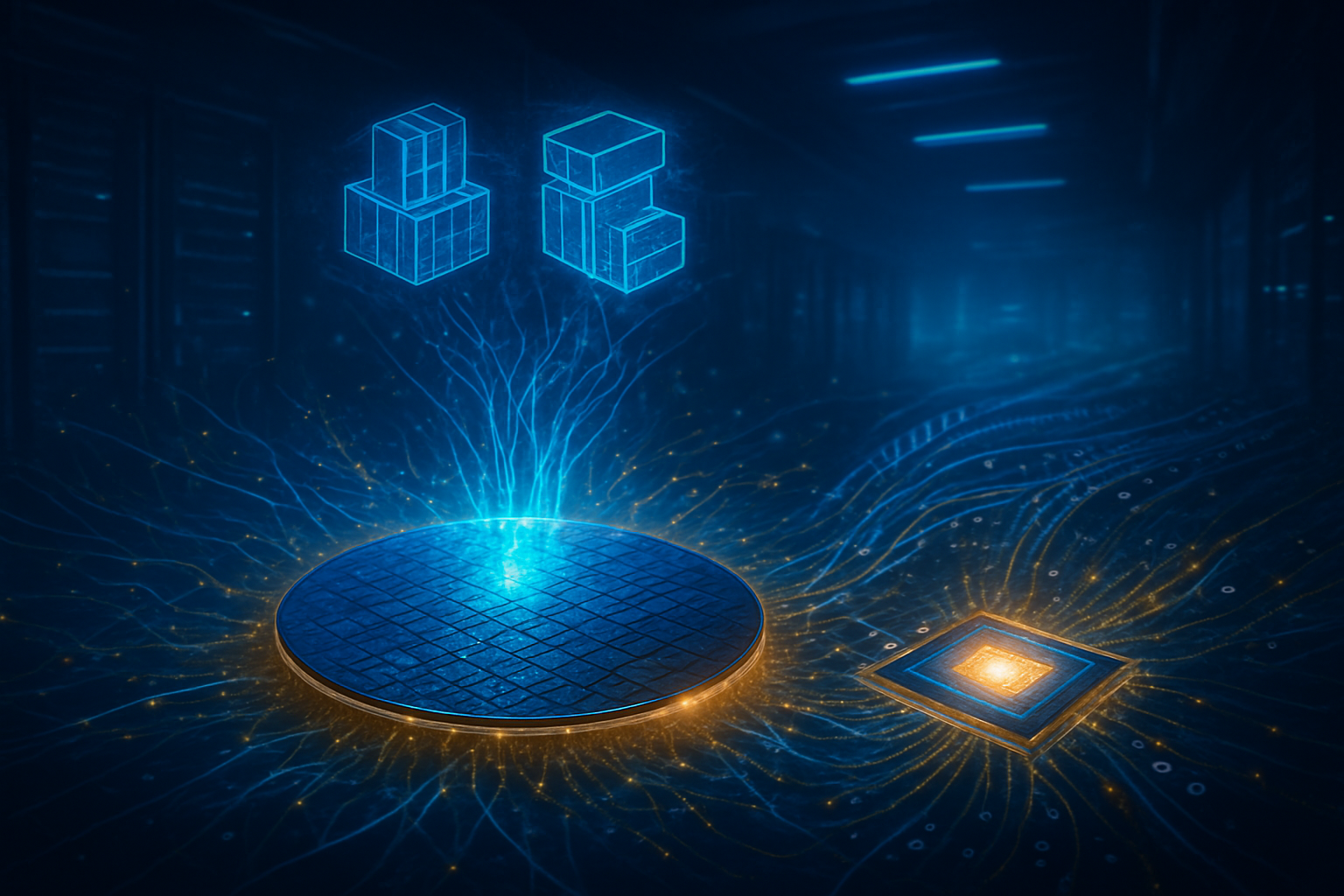
Looking toward late 2026 and 2027, the focus will shift from 2nm production to the stabilization of the A16 node. Experts predict that the next major challenge will be advanced packaging. While the transistors themselves are shrinking, the way they are stacked—using TSMC’s CoWoS (Chip on Wafer on Substrate) and SoIC (System on Integrated Chips) technologies—will be the key to performance gains. As chips become more complex, the packaging becomes a performance-limiting factor, leading TSMC to allocate nearly 20% of its massive CapEx budget to advanced packaging facilities.
In the near term, we can expect a "two-tier" AI market to emerge. Leading-edge companies will fight for A16 capacity to power massive frontier models, while the "rest of the world" migrates to N3 and N2 for more mature AI applications. The long-term roadmap already points toward the A14 (1.4nm) and A10 (1nm) nodes, which are rumored to explore new materials like two-dimensional (2D) semiconductors to replace silicon channels entirely.
Final Assessment: TSMC’s Unrivaled Momentum
TSMC’s Q4 results and its A16 roadmap demonstrate a company operating at the peak of its powers. By successfully managing the transition to GAAFET and pioneering backside power delivery, TSMC has effectively built a moat that will be incredibly difficult for Intel Foundry or Samsung to cross in the next three years. The AI segment's growth isn't just a revenue driver; it is the core identity of the company moving forward.
The significance of this development in AI history cannot be overstated. We are witnessing the physical manifestation of the scaling laws that govern artificial intelligence. For the coming months, watch for announcements regarding the first A16 tape-outs from NVIDIA and Apple, and keep a close eye on TSMC’s capacity expansion in Arizona and Japan, as these facilities will be crucial for diversifying the supply chain of the world's most critical technology.
This content is intended for informational purposes only and represents analysis of current AI developments.
TokenRing AI delivers enterprise-grade solutions for multi-agent AI workflow orchestration, AI-powered development tools, and seamless remote collaboration platforms.
For more information, visit https://www.tokenring.ai/.