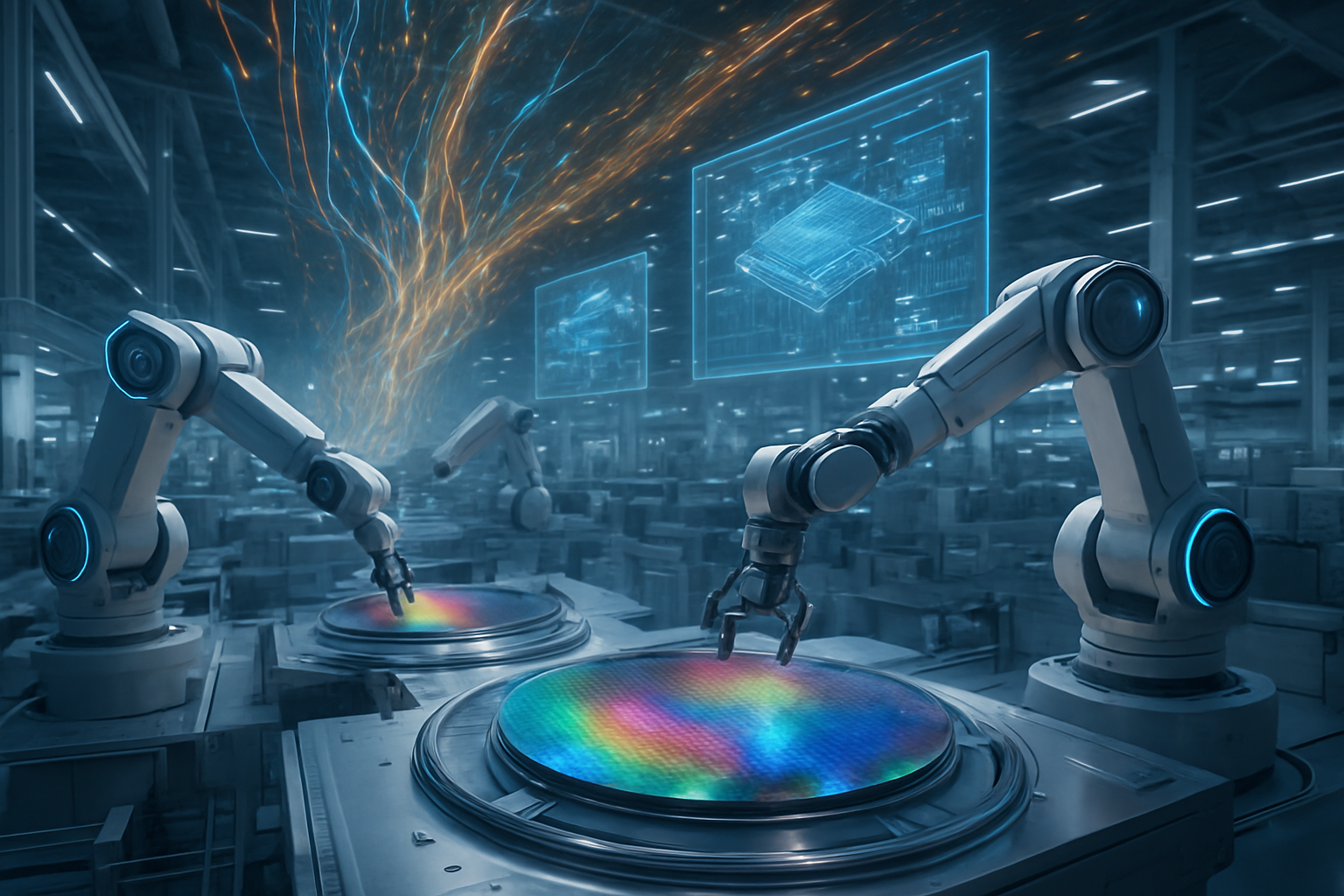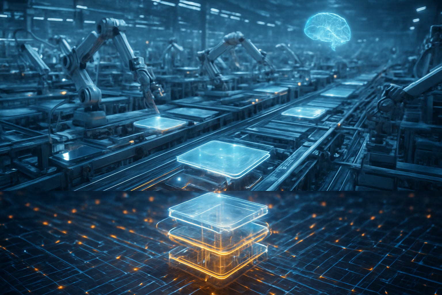
The semiconductor industry has officially crossed the threshold into the "Angstrom Era." Taiwan Semiconductor Manufacturing Company (NYSE:TSM), the world’s largest contract chipmaker, confirmed this week that its 2nm (N2) process technology has successfully transitioned into high-volume manufacturing (HVM) as of Q4 2025. With production lines humming in Hsinchu and Kaohsiung, the shift marks a historic departure from the FinFET architecture that defined the last decade of computing, ushering in the age of Nanosheet Gate-All-Around (GAA) transistors.
This milestone is more than a technical upgrade; it is the bedrock upon which the next generation of artificial intelligence is being built. As TSMC gears up for a record-breaking 2026, the company has signaled a massive $52 billion to $56 billion capital expenditure plan to satisfy an "insatiable" global demand for AI silicon. With the N2 ramp-up now in full swing and the revolutionary A16 node looming on the horizon for the second half of 2026, the foundry giant has effectively locked in its role as the primary gatekeeper of the AI revolution.
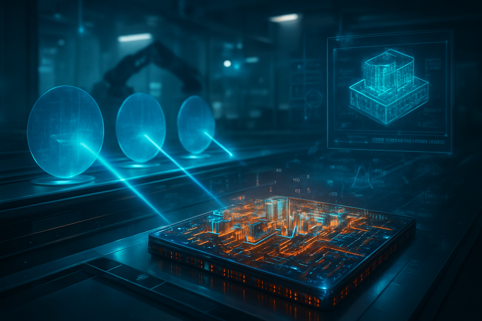
The technical leap from 3nm (N3E) to the 2nm (N2) node represents one of the most complex engineering feats in TSMC’s history. By implementing Nanosheet GAA transistors, TSMC has overcome the physical limitations of FinFET, allowing for better current control and significantly reduced power leakage. Initial data indicates that the N2 process delivers a 10% to 15% speed improvement at the same power level or a staggering 25% to 30% reduction in power consumption compared to the previous generation. This efficiency is critical for the AI industry, where power density has become the primary bottleneck for both data center scaling and edge device capabilities.
Looking toward the second half of 2026, TSMC is already preparing for the A16 node, which introduces the "Super Power Rail" (SPR). This backside power delivery system is a radical architectural shift that moves the power distribution network to the rear of the wafer. By decoupling the power and signal wires, TSMC can eliminate the need for space-consuming vias on the front side, allowing for even denser logic and more efficient energy delivery to the high-performance cores. The A16 node is specifically optimized for High-Performance Computing (HPC) and is expected to offer an additional 15% to 20% power efficiency gain over the enhanced N2P node.
The industry reaction to these developments has been one of calculated urgency. While competitors like Intel (NASDAQ:INTC) and Samsung (KRX:005930) are racing to deploy their own backside power and GAA solutions, TSMC’s successful HVM in Q4 2025 has provided a level of predictability that the AI research community thrives on. Leading AI labs have noted that the move to N2 and A16 will finally allow for "GPT-5 class" models to run natively on mobile hardware, while simultaneously doubling the efficiency of the massive H100 and B200 successor clusters currently dominating the cloud.
The primary beneficiaries of this 2nm transition are the "Magnificent Seven" and the specialized AI chip designers who have already reserved nearly all of TSMC’s initial N2 capacity. Apple (NASDAQ:AAPL) is widely expected to be the first to market with 2nm silicon in its late-2026 flagship devices, maintaining its lead in consumer-facing AI performance. Meanwhile, Nvidia (NASDAQ:NVDA) and AMD (NASDAQ:AMD) are reportedly pivoting their 2026 and 2027 roadmaps to prioritize the A16 node and its Super Power Rail feature for their flagship AI accelerators, aiming to keep pace with the power demands of increasingly large neural networks.
For major AI players like Microsoft (NASDAQ:MSFT) and Alphabet (NASDAQ:GOOGL), TSMC’s roadmap provides the necessary hardware runway to continue their aggressive expansion of generative AI services. These tech giants, which are increasingly designing their own custom AI ASICs (Application-Specific Integrated Circuits), depend on TSMC’s yield stability to manage their multi-billion dollar infrastructure investments. The $56 billion capex for 2026 suggests that TSMC is not just building more fabs, but is also aggressively expanding its CoWoS (Chip-on-Wafer-on-Substrate) advanced packaging capacity, which has been a major supply chain pain point for Nvidia in recent years.
However, the dominance of TSMC creates a high-stakes competitive environment for smaller startups. As TSMC implements a reported 3% to 10% price hike across its advanced nodes in 2026, the "cost of entry" for cutting-edge AI hardware is rising. Startups may find themselves forced into using older N3 or N5 nodes unless they can secure massive venture funding to compete for N2 wafer starts. This could lead to a strategic divide in the market: a few "silicon elites" with access to 2nm efficiency, and everyone else optimizing on legacy architectures.
The significance of TSMC’s 2026 expansion also carries a heavy geopolitical weight. The foundry’s progress in the United States has reached a critical turning point. Arizona Fab 1 successfully entered HVM in Q4 2024, producing 4nm and 5nm chips on American soil with yields that match those in Taiwan. With equipment installation for Arizona Fab 2 scheduled for Q3 2026, the vision of a diversified, resilient semiconductor supply chain is finally becoming a reality. This shift addresses a major concern for the AI ecosystem: the over-reliance on a single geographic point of failure.
In the broader AI landscape, the arrival of N2 and A16 marks the end of the "efficiency-by-software" era and the return of "efficiency-by-hardware." In the past few years, AI developers have focused on quantization and pruning to make models fit into existing memory and power budgets. With the massive gains offered by the Super Power Rail and Nanosheet transistors, hardware is once again leading the charge. This allows for a more ambitious scaling of model parameters, as the physical limits of thermal management in data centers are pushed back by another generation.
Comparisons to previous milestones, such as the move to 7nm or the introduction of EUV (Extreme Ultraviolet) lithography, suggest that the 2nm transition will have an even more profound impact. While 7nm enabled the initial wave of mobile AI, 2nm is the first node designed from the ground up to support the massive parallel processing required by Transformer-based models. The sheer scale of the $52-56 billion capex—nearly double the capex of most other global industrial leaders—underscores that we are in a unique historical moment where silicon capacity is the ultimate currency of national and corporate power.
As we look toward the remainder of 2026 and beyond, the focus will shift from the 2nm ramp to the maturation of the A16 node. The "Super Power Rail" is expected to become the industry standard for all high-performance silicon by 2027, forcing a complete redesign of motherboard and power supply architectures for servers. Experts predict that the first A16-based AI accelerators will hit the market in early 2027, potentially offering a 2x leap in training performance per watt, which would drastically reduce the environmental footprint of large-scale AI training.
The next major challenge on the horizon is the transition to the 1.4nm (A14) node, which TSMC is already researching in its R&D centers. Beyond 2026, the industry will have to grapple with the "memory wall"—the reality that logic speeds are outstripping the ability of memory to feed them data. This is why TSMC’s 2026 capex also heavily targets SoIC (System-on-Integrated-Chips) and other 3D-stacking technologies. The future of AI hardware is not just about smaller transistors, but about collapsing the physical distance between the processor and the memory.
In the near term, all eyes will be on the Q3 2026 equipment move-in at Arizona Fab 2. If TSMC can successfully replicate its 3nm and 2nm yields in the U.S., it will fundamentally change the strategic calculus for companies like Nvidia and Apple, who are under increasing pressure to "on-shore" their most sensitive AI workloads. Challenges remain, particularly regarding the high cost of electricity and labor in the U.S., but the momentum of the 2026 roadmap suggests that TSMC is willing to spend its way through these obstacles.
TSMC’s successful mass production of 2nm chips and its aggressive 2026 expansion plan represent a defining moment for the technology industry. By meeting its Q4 2025 HVM targets and laying out a clear path to the A16 node with Super Power Rail technology, the company has provided the AI hardware ecosystem with the certainty it needs to continue its exponential growth. The record-setting $52-56 billion capex is a bold bet on the longevity of the AI boom, signaling that the foundry sees no end in sight for the demand for advanced compute.
The significance of these developments in AI history cannot be overstated. We are moving from a period of "AI experimentation" to an era of "AI ubiquity," where the efficiency of the underlying silicon determines the viability of every product, from a digital assistant on a smartphone to a sovereign AI cloud for a nation-state. As TSMC solidifies its lead, the gap between it and its competitors appears to be widening, making the foundry not just a supplier, but the central architect of the digital future.
In the coming months, investors and tech analysts should watch for the first yield reports from the Kaohsiung N2 lines and the initial design tape-outs for the A16 process. These indicators will confirm whether TSMC can maintain its breakneck pace or if the physical limits of the Angstrom era will finally slow the march of Moore’s Law. For now, however, the crown remains firmly in Hsinchu, and the AI revolution is running on TSMC silicon.
This content is intended for informational purposes only and represents analysis of current AI developments.
TokenRing AI delivers enterprise-grade solutions for multi-agent AI workflow orchestration, AI-powered development tools, and seamless remote collaboration platforms.
For more information, visit https://www.tokenring.ai/.