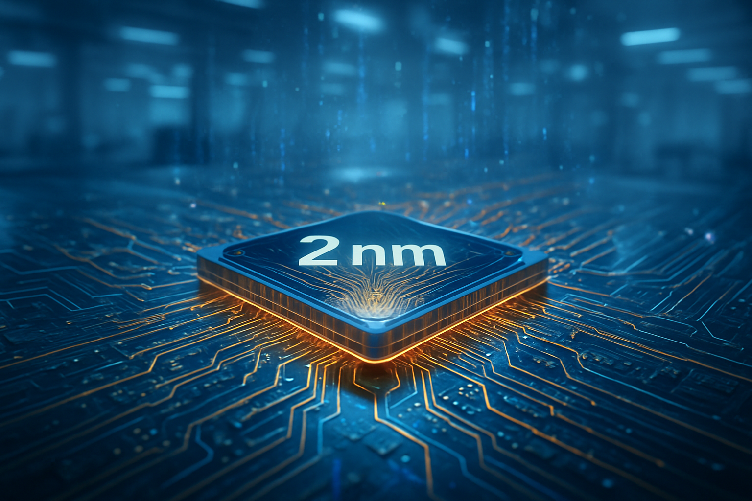
The semiconductor landscape has officially shifted into a new era. As of January 9, 2026, Taiwan Semiconductor Manufacturing Company (NYSE:TSM) has successfully commenced the high-volume manufacturing of its 2-nanometer (N2) process node. This milestone marks the most significant architectural change in chip design in over a decade, as the industry moves away from the traditional FinFET structure to the cutting-edge Gate-All-Around (GAA) nanosheet technology.
The immediate significance of this transition cannot be overstated. By shrinking transistors to the 2nm scale, TSMC is providing the foundational hardware necessary to power the next generation of artificial intelligence, high-performance computing (HPC), and mobile devices. With volume production now ramping up at Fab 20 in Hsinchu and Fab 22 in Kaohsiung, the first wave of 2nm-powered consumer electronics is expected to hit the market later this year, spearheaded by an exclusive capacity lock from the world’s most valuable technology company.
Technical Foundations: The GAA Nanosheet Breakthrough
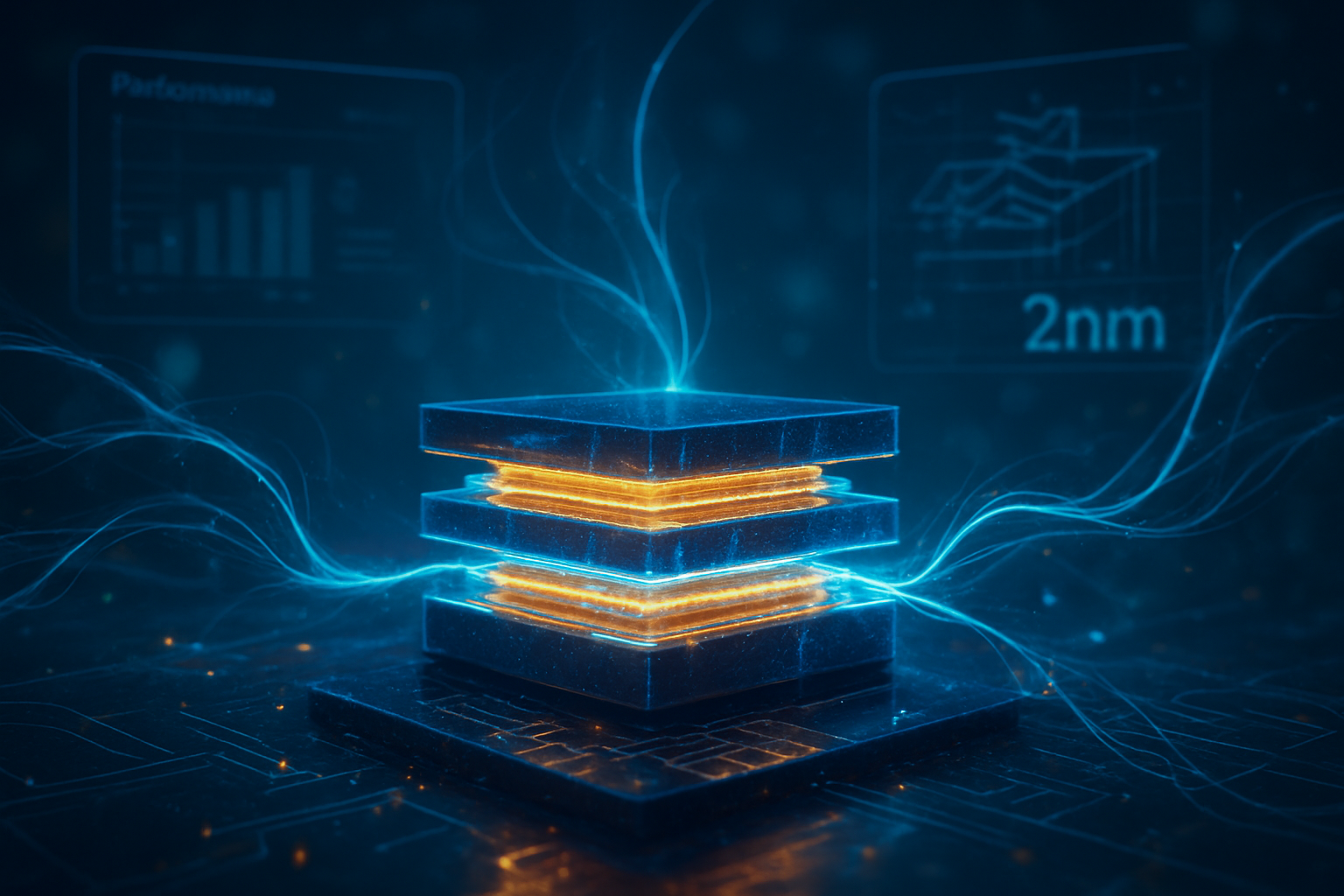
The N2 node represents a departure from the "Fin" architecture that has dominated the industry since 2011. In the new GAA nanosheet design, the transistor gate surrounds the channel on all four sides. This provides superior electrostatic control, which drastically reduces current leakage—a persistent problem as transistors have become smaller and more densely packed. By wrapping the gate around the entire channel, TSMC can more precisely manage the flow of electrons, leading to a substantial leap in efficiency and performance.
Technically, the N2 node offers a compelling value proposition over its predecessor, the 3nm (N3E) node. According to TSMC’s engineering data, the 2nm process delivers a 10% to 15% speed improvement at the same power consumption level, or a 25% to 30% reduction in power usage at the same clock speed. Furthermore, the node provides a 1.15x increase in chip density, allowing engineers to cram more logic and memory into the same physical footprint. This is particularly critical for AI accelerators, where transistor density directly correlates with the ability to process massive neural networks.
Initial reactions from the semiconductor research community have been overwhelmingly positive, particularly regarding TSMC’s reported yield rates. While transitions to new architectures often suffer from low initial yields, reports indicate that TSMC has achieved nearly 70% yield during the early mass-production phase. This maturity distinguishes TSMC from its competitors, who have struggled to maintain stability while transitioning to GAA. Experts note that while the N2 node does not yet include backside power delivery—a feature reserved for the upcoming N2P variant—it introduces Super High-Performance Metal-Insulator-Metal (SHPMIM) capacitors, which double capacitance density to stabilize power delivery for high-load AI tasks.
The Business of Silicon: Apple’s Strategic Dominance
The launch of the N2 node has ignited a fierce strategic battle among tech giants, with Apple (NASDAQ:AAPL) emerging as the clear winner in the initial scramble for capacity. Apple has reportedly secured over 50% of TSMC’s total 2nm output through 2026. This massive "capacity lock" ensures that the upcoming iPhone 18 series, likely powered by the A20 Pro chip, will be the first consumer device to utilize 2nm silicon. By monopolizing the early supply, Apple creates a multi-year barrier for competitors, as rivals like Qualcomm (NASDAQ:QCOM) and MediaTek may have to wait until 2027 to access equivalent volumes of N2 wafers.
This development places other industry leaders in a complex position. NVIDIA (NASDAQ:NVDA) and AMD (NASDAQ:AMD) are both high-priority customers for TSMC, but they are increasingly competing for the remaining 2nm capacity to fuel their next-generation AI GPUs and data center processors. The scarcity of 2nm wafers could lead to a tiered market where only the highest-margin products—such as NVIDIA’s Blackwell successors or AMD’s Instinct accelerators—can afford the premium pricing associated with the new node.
For the broader market, TSMC’s success reinforces its position as the indispensable linchpin of the global tech economy. While Samsung (KRX:005930) was technically the first to introduce GAA with its 3nm node, it has faced persistent yield bottlenecks that have deterred major customers. Meanwhile, Intel (NASDAQ:INTC) is making a bold play with its 18A node, which features "PowerVia" backside power delivery. While Intel 18A may offer competitive raw performance, TSMC’s massive ecosystem and proven track record of high-volume reliability give it a strategic advantage that is currently unmatched in the foundry business.
Global Implications: AI and the Energy Crisis
The arrival of 2nm technology is a pivotal moment for the AI industry, which is currently grappling with the dual challenges of computing demand and energy consumption. As AI models grow in complexity, the power required to train and run them has skyrocketed, leading to concerns about the environmental impact of massive data centers. The 30% power efficiency gain offered by the N2 node provides a vital "pressure release valve," allowing AI companies to scale their operations without a linear increase in electricity usage.
Furthermore, the 2nm milestone represents a continuation of Moore’s Law at a time when many predicted its demise. The shift to GAA nanosheets proves that through material science and architectural innovation, the industry can continue to shrink transistors and improve performance. However, this progress comes at a staggering cost. The price of a single 2nm wafer is estimated to be significantly higher than 3nm, potentially leading to a "silicon divide" where only the largest tech conglomerates can afford the most advanced hardware.
Compared to previous milestones, such as the jump from 7nm to 5nm, the 2nm transition is more than just a shrink; it is a fundamental redesign of how electricity moves through a chip. This shift is essential for the "Edge AI" movement—bringing powerful, local AI processing to smartphones and wearable devices without draining their batteries in minutes. The success of the N2 node will likely determine which companies lead the next decade of ambient computing and autonomous systems.
The Road Ahead: N2P and the 1.4nm Horizon
Looking toward the near-term future, TSMC is already preparing for the next iteration of the 2nm platform. The N2P node, expected to enter production in late 2026, will introduce backside power delivery. This technology moves the power distribution network to the back of the silicon wafer, separating it from the signal wires on the front. This reduces interference and allows for even higher performance, setting the stage for the true peak of the 2nm era.
Beyond 2026, the roadmap points toward the A14 (1.4nm) node. Research and development for A14 are already underway, with expectations that it will push the limits of extreme ultraviolet (EUV) lithography. The primary challenge moving forward will not just be the physics of the transistors, but the complexity of the packaging. TSMC’s CoWoS (Chip-on-Wafer-on-Substrate) and other 3D packaging technologies will become just as important as the node itself, as engineers look to stack 2nm chips to achieve unprecedented levels of performance.
Experts predict that the next two years will see a "Foundry War" as Intel and Samsung attempt to reclaim market share from TSMC. Intel’s 18A is the most credible threat TSMC has faced in years, and the industry will be watching closely to see if Intel can deliver on its promise of "five nodes in four years." If Intel succeeds, it could break TSMC’s near-monopoly on advanced logic; if it fails, TSMC’s dominance will be absolute for the remainder of the decade.
Conclusion: A New Standard for Excellence
The commencement of 2nm volume production at TSMC is a defining moment for the technology industry in 2026. By successfully transitioning to GAA nanosheet transistors and securing the backing of industry titans like Apple, TSMC has once again set the gold standard for semiconductor manufacturing. The technical gains in power efficiency and performance will ripple through every sector of the economy, from the smartphones in our pockets to the massive AI clusters shaping the future of human knowledge.
As we move through the first quarter of 2026, the key metrics to watch will be the continued ramp-up of wafer output and the performance benchmarks of the first 2nm chips. While challenges remain—including geopolitical tensions and the rising cost of fabrication—the successful launch of the N2 node ensures that the engine of digital innovation remains in high gear. The era of 2nm has arrived, and with it, the promise of a more efficient, powerful, and AI-driven future.
This content is intended for informational purposes only and represents analysis of current AI developments.
TokenRing AI delivers enterprise-grade solutions for multi-agent AI workflow orchestration, AI-powered development tools, and seamless remote collaboration platforms.
For more information, visit https://www.tokenring.ai/.