Tag: 2nm

  • TSMC Enters the 2nm Era: Volume Production Officially Begins at Fab 22

    TSMC Enters the 2nm Era: Volume Production Officially Begins at Fab 22

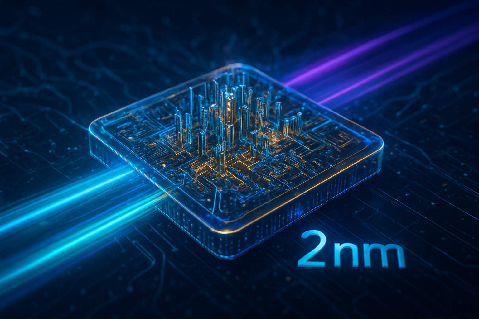
    KAOHSIUNG, Taiwan — In a landmark moment for the semiconductor industry, Taiwan Semiconductor Manufacturing Company (NYSE:TSM) has officially commenced volume production of its next-generation 2nm (N2) process technology. The rollout is centered at the newly operational Fab 22 in the Nanzih Science Park of Kaohsiung, marking the most significant architectural shift in chip manufacturing in over a decade. As of December 31, 2025, TSMC has successfully transitioned from the long-standing FinFET (Fin Field-Effect Transistor) structure to a sophisticated Gate-All-Around (GAA) nanosheet architecture, setting a new benchmark for the silicon that will power the next wave of artificial intelligence.

    The commencement of 2nm production arrives at a critical juncture for the global tech economy. With the demand for AI-specific compute power reaching unprecedented levels, the N2 node promises to provide the efficiency and density required to sustain the current pace of AI innovation. Initial reports from the Kaohsiung facility indicate that yield rates have already surpassed 65%, a remarkably high figure for a first-generation GAA node, signaling that TSMC is well-positioned to meet the massive order volumes expected from industry leaders in 2026.

    The Nanosheet Revolution: Inside the N2 Process

    The transition to the N2 node represents more than just a reduction in size; it is a fundamental redesign of how transistors function. For the past decade, the industry has relied on FinFET technology, where the gate sits on three sides of the channel. However, as transistors shrunk below 3nm, FinFETs began to struggle with current leakage and power efficiency. The new GAA nanosheet architecture at Fab 22 solves this by surrounding the channel on all four sides with the gate. This provides superior electrostatic control, drastically reducing power leakage and allowing for finer tuning of performance characteristics.

    Technically, the N2 node is a powerhouse. Compared to the previous N3E (enhanced 3nm) process, the 2nm technology is expected to deliver a 10-15% performance boost at the same power level, or a staggering 25-30% reduction in power consumption at the same speed. Furthermore, the N2 process introduces super-high-performance metal-insulator-metal (SHPMIM) capacitors, which double the capacitance density. This advancement significantly improves power stability, a crucial requirement for high-performance computing (HPC) and AI accelerators that operate under heavy, fluctuating workloads.

    Industry experts and researchers have reacted with cautious optimism. While the shift to GAA was long anticipated, the successful volume ramp-up at Fab 22 suggests that TSMC has overcome the complex lithography and materials science challenges that have historically delayed such transitions. "The move to nanosheets is the 'make-or-break' moment for sub-2nm scaling," noted one senior semiconductor analyst. "TSMC’s ability to hit volume production by the end of 2025 gives them a significant lead in providing the foundational hardware for the next decade of AI."

    A Strategic Leap for AMD and the AI Hardware Race

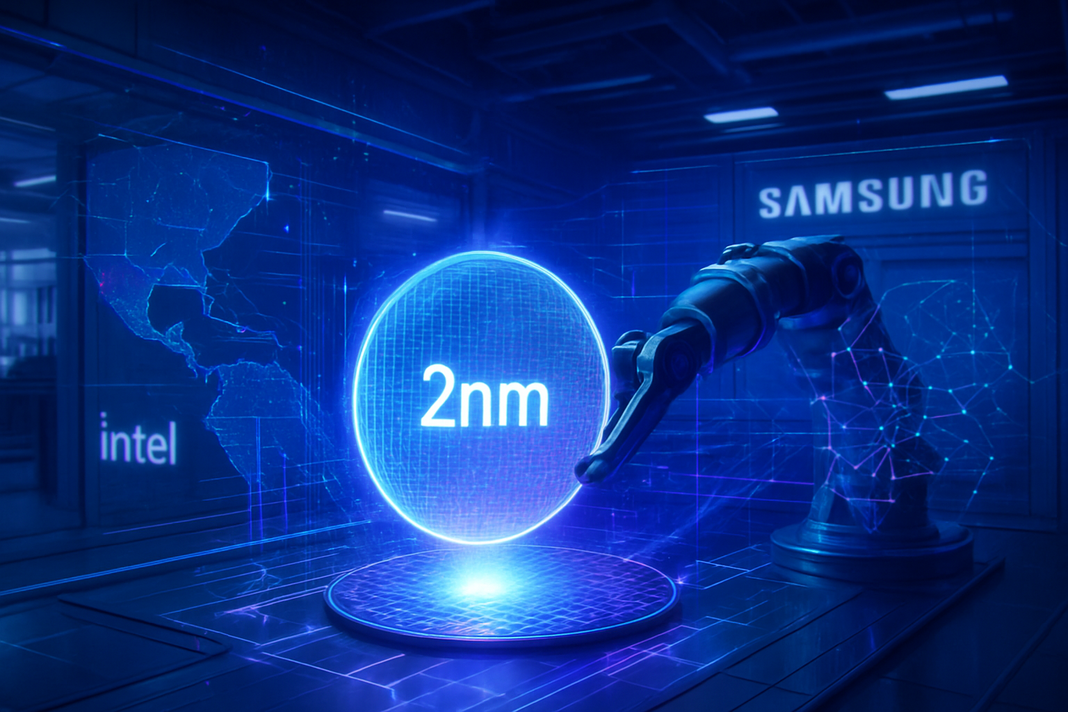
    The immediate beneficiary of this milestone is Advanced Micro Devices (NASDAQ:AMD), which has already confirmed its role as a lead customer for the N2 node. AMD plans to utilize the 2nm process for its upcoming Zen 6 "Venice" CPUs and the highly anticipated Instinct MI450 AI accelerators. By securing 2nm capacity, AMD aims to gain a competitive edge over its primary rival, NVIDIA (NASDAQ:NVDA). While NVIDIA’s upcoming "Rubin" architecture is expected to remain on a refined 3nm-class node, AMD’s shift to 2nm for its MI450 core dies could offer superior energy efficiency and compute density—critical metrics for the massive data centers operated by companies like OpenAI and Microsoft (NASDAQ:MSFT).

    The impact extends beyond AMD. Apple (NASDAQ:AAPL), traditionally TSMC's largest customer, is expected to transition its "Pro" series silicon to the N2 node for the 2026 iPhone and Mac refreshes. The strategic advantage of 2nm is clear: it allows device manufacturers to either extend battery life significantly or pack more neural processing units (NPUs) into the same thermal envelope. For the burgeoning market of AI PCs and AI-integrated smartphones, this efficiency is the "holy grail" that enables on-device LLMs (Large Language Models) to run without draining battery life in minutes.

    Meanwhile, the competition is intensifying. Intel (NASDAQ:INTC) is racing to catch up with its 18A process, which also utilizes a GAA-style architecture (RibbonFET), while Samsung (KRX:005930) has been producing GAA-based chips at 3nm with mixed success. TSMC’s successful volume production at Fab 22 reinforces its dominance, providing a stable, high-yield platform that major tech giants prefer for their flagship products. The "GIGAFAB" status of Fab 22 ensures that as demand for 2nm scales, TSMC will have the physical footprint to keep pace with the exponential growth of AI infrastructure.

    Redefining the AI Landscape and the Sustainability Challenge

    The broader significance of the 2nm era lies in its potential to address the "AI energy crisis." As AI models grow in complexity, the energy required to train and run them has become a primary concern for both tech companies and environmental regulators. The 25-30% power reduction offered by the N2 node is not just a technical spec; it is a necessary evolution to keep the AI industry sustainable. By allowing data centers to perform more operations per watt, TSMC is effectively providing a release valve for the mounting pressure on global energy grids.

    Furthermore, this milestone marks a continuation of Moore's Law, albeit through increasingly complex and expensive means. The transition to GAA at Fab 22 proves that silicon scaling still has room to run, even as we approach the physical limits of the atom. However, this progress comes with a "geopolitical premium." The concentration of 2nm production in Taiwan, particularly at the new Kaohsiung hub, underscores the world's continued reliance on a single geographic point for its most advanced technology. This has prompted ongoing discussions about supply chain resilience and the strategic importance of TSMC's expanding global footprint, including its future sites in Arizona and Japan.

    Comparatively, the jump to 2nm is being viewed as a more significant leap than the transition from 5nm to 3nm. While 3nm was an incremental improvement of the FinFET design, 2nm is a "clean sheet" approach. This architectural reset allows for a level of design flexibility—such as varying nanosheet widths—that will enable chip designers to create highly specialized silicon for specific AI tasks, ranging from ultra-low-power edge devices to massive, multi-die AI training clusters.

    The Road to 1nm: What Lies Ahead

    Looking toward the future, the N2 node is just the beginning of a multi-year roadmap. TSMC has already signaled that an enhanced version, N2P, will follow in late 2026, featuring backside power delivery—a technique that moves power lines to the rear of the wafer to reduce interference and further boost performance. Beyond that, the company is already laying the groundwork for the A16 (1.6nm) node, which is expected to integrate "Super Power Rail" technology and utilize High-NA EUV (Extreme Ultraviolet) lithography machines.

    In the near term, the industry will be watching the performance of the first Zen 6 and MI450 samples. If these chips deliver the 70% performance gains over current generations that some analysts predict, it could trigger a massive upgrade cycle across the enterprise and consumer sectors. The challenge for TSMC and its partners will be managing the sheer complexity of these designs. As features shrink, the risk of "silent data errors" and manufacturing defects increases, requiring even more advanced testing and packaging solutions like CoWoS (Chip-on-Wafer-on-Substrate).

    The next 12 to 18 months will be a period of intense validation. As Fab 22 ramps up to full capacity, the tech world will finally see if the promises of the 2nm era translate into a tangible acceleration of AI capabilities. If successful, the GAA transition will be remembered as the moment that gave AI the "silicon lungs" it needed to breathe and grow into its next phase of evolution.

    Conclusion: A New Chapter in Silicon History

    The official start of 2nm volume production at TSMC’s Fab 22 is a watershed moment. It represents the culmination of billions of dollars in R&D and years of engineering effort to move past the limitations of FinFET. By successfully launching the industry’s first high-volume GAA nanosheet process, TSMC has not only secured its market leadership but has also provided the essential hardware foundation for the next generation of AI-driven products.

    The key takeaways are clear: the AI industry now has a path to significantly higher efficiency and performance, AMD and Apple are poised to lead the charge in 2026, and the technical hurdles of GAA have been largely cleared. As we move into 2026, the focus will shift from "can it be built?" to "how fast can it be deployed?" The silicon coming out of Kaohsiung today will be the brains of the world's most advanced AI systems tomorrow.

    In the coming weeks, watch for further announcements regarding TSMC’s yield stability and potential additional lead customers joining the 2nm roster. The era of the nanosheet has begun, and the tech landscape will never be the same.


    This content is intended for informational purposes only and represents analysis of current AI developments.

    TokenRing AI delivers enterprise-grade solutions for multi-agent AI workflow orchestration, AI-powered development tools, and seamless remote collaboration platforms.
    For more information, visit https://www.tokenring.ai/.

  • TSMC Commences 2nm Volume Production: The Next Frontier of AI Silicon

    TSMC Commences 2nm Volume Production: The Next Frontier of AI Silicon

    HSINCHU, Taiwan — In a move that solidifies its absolute dominance over the global semiconductor landscape, Taiwan Semiconductor Manufacturing Company (NYSE: TSM) has officially commenced high-volume manufacturing (HVM) of its 2-nanometer (N2) process node as of the fourth quarter of 2025. This milestone marks the industry's first successful transition to Gate-all-around Field-Effect Transistor (GAAFET) architecture at scale, providing the foundational hardware necessary to power the next generation of generative AI models and hyper-efficient mobile devices.

    The commencement of N2 production is not merely a generational shrink; it represents a fundamental re-engineering of the transistor itself. By moving away from the FinFET structure that has defined the industry for over a decade, TSMC is addressing the physical limitations of silicon at the atomic scale. As of late December 2025, the company’s facilities in Baoshan and Kaohsiung are operating at full tilt, signaling a new era of "AI Silicon" that promises to break the energy-efficiency bottlenecks currently stifling data center expansion and edge computing.

    Technical Mastery: GAAFET and the 70% Yield Milestone

    The technical leap from 3nm (N3P) to 2nm (N2) is defined by the implementation of "nanosheet" GAAFET technology. Unlike traditional FinFETs, where the gate covers three sides of the channel, the N2 architecture features a gate that completely surrounds the channel on all four sides. This provides superior electrostatic control, drastically reducing sub-threshold leakage—a critical issue as transistors approach the size of individual molecules. TSMC reports that this transition has yielded a 10–15% performance gain at the same power envelope, or a staggering 25–30% reduction in power consumption at the same clock speeds compared to its refined 3nm process.

    Perhaps the most significant technical achievement is the reported 70% yield rate for logic chips at the Baoshan (Hsinchu) and Kaohsiung facilities. For a brand-new node using a novel transistor architecture, a 70% yield is considered exceptionally high, far outstripping the early-stage yields of competitors. This success is attributed to TSMC's "NanoFlex" technology, which allows chip designers to mix and match different nanosheet widths within a single design, optimizing for either high performance or extreme power efficiency depending on the specific block’s requirements.

    Initial reactions from the AI research community and hardware engineers have been overwhelmingly positive. Experts note that the 25-30% power reduction is the "holy grail" for the next phase of AI development. As large language models (LLMs) move toward "on-device" execution, the thermal constraints of smartphones and laptops have become the primary limiting factor. The N2 node effectively provides the thermal headroom required to run sophisticated neural engines without compromising battery life or device longevity.

    Market Dominance: Apple and Nvidia Lead the Charge

    The immediate beneficiaries of this production ramp are the industry’s "Big Tech" titans, most notably Apple (NASDAQ: AAPL) and Nvidia (NASDAQ: NVDA). While Apple’s latest A19 Pro chips utilized a refined 3nm process, the company has reportedly secured the lion's share of TSMC’s initial 2nm capacity for its 2026 product cycle. This strategic "pre-booking" ensures that Apple maintains a hardware lead in consumer AI, potentially allowing for the integration of more complex "Apple Intelligence" features that run natively on the A20 chip.

    For Nvidia, the shift to 2nm is vital for the roadmap beyond its current Blackwell and Rubin architectures. While the standard Rubin GPUs are built on 3nm, the upcoming "Rubin Ultra" and the successor "Feynman" architecture are expected to leverage the N2 and subsequent A16 nodes. The power efficiency of 2nm is a strategic advantage for Nvidia, as data center operators are increasingly limited by power grid capacity rather than floor space. By delivering more TFLOPS per watt, Nvidia can maintain its market lead against rivals like Advanced Micro Devices (NASDAQ: AMD) and Intel (NASDAQ: INTC).

    The competitive implications for Intel and Samsung (KRX: 005930) are stark. While Intel’s 18A node aims to compete with TSMC’s 2nm by introducing "PowerVia" (backside power delivery) earlier, TSMC’s superior yield rates and massive manufacturing scale remain a formidable moat. Samsung, despite being the first to move to GAAFET at 3nm, has reportedly struggled with yield consistency, leading major clients like Qualcomm (NASDAQ: QCOM) to remain largely within the TSMC ecosystem for their flagship Snapdragon processors.

    The Wider Significance: Breaking the AI Energy Wall

    Looking at the broader AI landscape, the commencement of 2nm production arrives at a critical juncture. The industry has been grappling with the "energy wall"—the point at which the power requirements for training and deploying AI models become economically and environmentally unsustainable. TSMC’s N2 node provides a much-needed reprieve, potentially extending the viability of the current scaling laws that have driven AI progress over the last three years.

    This milestone also highlights the increasing "silicon-centric" nature of geopolitics. The successful ramp-up at the Kaohsiung facility, which was accelerated by six months, underscores Taiwan’s continued role as the indispensable hub of the global technology supply chain. However, it also raises concerns regarding the concentration of advanced manufacturing. As AI becomes a foundational utility for modern economies, the reliance on a single company for the most advanced 2nm chips creates a single point of failure that global policymakers are still struggling to address through initiatives like the U.S. CHIPS Act.

    Comparisons to previous milestones, such as the move to FinFET at 16nm or the introduction of EUV (Extreme Ultraviolet) lithography at 7nm, suggest that the 2nm transition will have a decade-long tail. Just as those breakthroughs enabled the smartphone revolution and the first wave of cloud computing, the N2 node is the literal "bedrock" upon which the agentic AI era will be built. It transforms AI from a cloud-based service into a ubiquitous, energy-efficient local presence.

    Future Horizons: N2P, A16, and the Road to 1.6nm

    TSMC’s roadmap does not stop at the base N2 node. The company has already detailed the "N2P" process, an enhanced version of 2nm scheduled for 2026, which will introduce Backside Power Delivery (BSPDN). This technology moves the power rails to the rear of the wafer, further reducing voltage drop and freeing up space for signal routing. Following N2P, the "A16" node (1.6nm) is expected to debut in late 2026 or early 2027, promising another 10% performance jump and even more sophisticated power delivery systems.

    The potential applications for this silicon are vast. Beyond smartphones and AI accelerators, the 2nm node is expected to revolutionize autonomous driving systems, where real-time processing of sensor data must be balanced with the limited battery capacity of electric vehicles. Furthermore, the efficiency gains of N2 could enable a new generation of sophisticated AR/VR glasses that are light enough for all-day wear while possessing the compute power to render complex digital overlays in real-time.

    Challenges remain, particularly regarding the astronomical cost of these chips. With 2nm wafers estimated to cost nearly $30,000 each, the "cost-per-transistor" trend is no longer declining as rapidly as it once did. Experts predict that this will lead to a surge in "chiplet" designs, where only the most critical compute elements are built on 2nm, while less sensitive components are relegated to older, cheaper nodes.

    A New Standard for the Silicon Age

    The official commencement of 2nm volume production at TSMC is a defining moment for the late 2025 tech landscape. By successfully navigating the transition to GAAFET architecture and achieving a 70% yield at its Baoshan and Kaohsiung sites, TSMC has once again moved the goalposts for the entire semiconductor industry. The 10-15% performance gain and 25-30% power reduction are the essential ingredients for the next evolution of artificial intelligence.

    In the coming months, the industry will be watching for the first "tape-outs" of consumer silicon from Apple and the first high-performance computing (HPC) samples from Nvidia. As these 2nm chips begin to filter into the market throughout 2026, the gap between those who have access to TSMC’s leading-edge capacity and those who do not will likely widen, further concentrating power among the elite tier of AI developers.

    Ultimately, the N2 node represents the triumph of precision engineering over the daunting physics of the sub-atomic world. As we look toward the 1.6nm A16 era, it is clear that while Moore's Law may be slowing, the ingenuity of the semiconductor industry continues to provide the horsepower necessary for the AI revolution to reach its full potential.


    This content is intended for informational purposes only and represents analysis of current AI developments.

    TokenRing AI delivers enterprise-grade solutions for multi-agent AI workflow orchestration, AI-powered development tools, and seamless remote collaboration platforms.
    For more information, visit https://www.tokenring.ai/.

  • The 2nm Bottleneck: Apple Secures Lion’s Share of TSMC’s Next-Gen Capacity as Industry Braces for Scarcity

    The 2nm Bottleneck: Apple Secures Lion’s Share of TSMC’s Next-Gen Capacity as Industry Braces for Scarcity

    As 2025 draws to a close, the semiconductor industry is entering a period of unprecedented supply-side tension. Taiwan Semiconductor Manufacturing Company (NYSE: TSM) has officially signaled a "capacity crunch" for its upcoming 2nm (N2) process node, revealing that production slots are effectively sold out through the end of 2026. In a move that mirrors its previous dominance of the 3nm node, Apple (NASDAQ: AAPL) has reportedly secured over 50% of the initial 2nm volume, leaving a roster of high-performance computing (HPC) giants and mobile competitors to fight for the remaining fabrication windows.

    This scarcity marks a critical juncture for the artificial intelligence and consumer electronics sectors. With the first 2nm-powered devices expected to hit the market in late 2026, the bottleneck at TSMC is no longer just a manufacturing hurdle—it is a strategic gatekeeper. For companies like NVIDIA (NASDAQ: NVDA) and AMD (NASDAQ: AMD), the limited availability of 2nm wafers is forcing a recalibration of product roadmaps, as the industry grapples with the escalating costs and technical complexities of the most advanced silicon on the planet.

    The N2 Leap: GAAFET and the End of the FinFET Era

    The transition to the N2 node represents TSMC’s most significant architectural shift in over a decade. After years of refining the FinFET (Fin Field-Effect Transistor) structure, the foundry is officially moving to Gate-All-Around FET (GAAFET) technology, specifically utilizing a nanosheet architecture. In this design, the gate surrounds the channel on all four sides, providing vastly superior electrostatic control. This technical pivot is essential for maintaining the pace of Moore’s Law, as it significantly reduces current leakage—a primary obstacle in the sub-3nm era.

    Technically, the N2 node delivers substantial gains over the current N3E (3nm) standard. Early performance metrics indicate a 10–15% speed improvement at the same power levels, or a 25–30% reduction in power consumption at the same clock speeds. Furthermore, transistor density is expected to increase by approximately 1.1x. However, this first generation of 2nm will not yet include "Backside Power Delivery"—a feature TSMC calls the "Super Power Rail." That innovation is reserved for the N2P and A16 (1.6nm) nodes, which are slated for late 2026 and 2027, respectively.

    Initial reactions from the semiconductor research community have been a mix of awe and caution. While the efficiency gains of GAAFET are undeniable, the cost of entry has reached a fever pitch. Reports suggest that 2nm wafers are priced at approximately $30,000 per unit—a 50% premium over 3nm wafers. Industry experts note that while Apple can absorb these costs by positioning its A20 and M6 chips as premium offerings, smaller players may find the financial barrier to 2nm entry nearly insurmountable, potentially widening the gap between the "silicon elite" and the rest of the market.

    The Capacity War: Apple’s Dominance and the Ripple Effect

    Apple’s aggressive booking of over half of TSMC’s 2nm capacity for 2026 serves as a defensive moat against its competitors. By locking down the A20 chip production for the iPhone 18 series, Apple ensures it will be the first to offer consumer-grade 2nm hardware. This strategy also extends to its Mac and Vision Pro lines, with the M6 and R2 chips expected to utilize the same N2 capacity. This "buyout" strategy forces other tech giants to scramble for what remains, creating a high-stakes queue that favors those with the deepest pockets.

    The implications for the AI hardware market are particularly profound. NVIDIA, which has been the primary beneficiary of the AI boom, has reportedly had to adjust its "Rubin" GPU architecture plans. While the highest-end variants of the Rubin Ultra may eventually see 2nm production, the bulk of the initial Rubin (R100) volume is expected to remain on refined 3nm nodes due to the 2nm supply constraints. Similarly, AMD is facing a tight window for its Zen 6 "Venice" processors; while AMD was among the first to tape out 2nm designs, its ability to scale those products in 2026 will be severely limited by Apple’s massive footprint at TSMC’s Hsinchu and Kaohsiung fabs.

    This crunch has led to a renewed interest in secondary sourcing. Both AMD and Google (NASDAQ: GOOGL) are reportedly evaluating Samsung’s (KRX: 005930) 2nm (SF2) process as a potential alternative. However, yield concerns continue to plague Samsung, leaving TSMC as the only reliable provider for high-volume, leading-edge silicon. For startups and mid-sized AI labs, the 2nm crunch means that access to the most efficient "AI at the edge" hardware will be delayed, potentially slowing the deployment of sophisticated on-device AI models that require the power-per-watt efficiency only 2nm can provide.

    Silicon Geopolitics and the AI Landscape

    The 2nm capacity crunch is more than a supply chain issue; it is a reflection of the broader AI landscape's insatiable demand for compute. As AI models migrate from massive data centers to local devices—a trend often referred to as "Edge AI"—the efficiency of the underlying silicon becomes the primary differentiator. The N2 node is the first process designed from the ground up to support the power envelopes required for running multi-billion parameter models on smartphones and laptops without devastating battery life.

    This development also highlights the increasing concentration of technological power. With TSMC remaining the sole provider of viable 2nm logic, the world’s most advanced AI and consumer tech roadmaps are tethered to a handful of square miles in Taiwan. While TSMC is expanding its Arizona (Fab 21) operations, high-volume 2nm production in the United States is not expected until at least 2027. This geographic concentration remains a point of concern for global supply chain resilience, especially as geopolitical tensions continue to simmer.

    Comparatively, the move to 2nm feels like the "Great 3nm Scramble" of 2023, but with higher stakes. In the previous cycle, the primary driver was traditional mobile performance. Today, the driver is the "AI PC" and "AI Phone" revolution. The ability to run generative AI locally is seen as the next major growth engine for the tech industry, and the 2nm node is the essential fuel for that engine. The fact that capacity is already booked through 2026 suggests that the industry expects the AI-driven upgrade cycle to be both long and aggressive.

    Looking Ahead: From N2 to the 1.4nm Frontier

    As TSMC ramps up its Fab 20 in Hsinchu and Fab 22 in Kaohsiung to meet the 2nm demand, the roadmap beyond 2026 is already taking shape. The near-term focus will be the introduction of N2P, which will integrate the much-anticipated Backside Power Delivery. This refinement is expected to offer an additional 5-10% performance boost by moving the power distribution network to the back of the wafer, freeing up more space for signal routing on the front.

    Looking further out, TSMC has already begun discussing the A14 (1.4nm) node, which is targeted for 2027 and 2028. This next frontier will likely involve High-NA (Numerical Aperture) EUV lithography, a technology that Intel (NASDAQ: INTC) has been aggressively pursuing to regain its "process leadership" crown. The competition between TSMC’s N2/A14 and Intel’s 18A/14A processes will define the next five years of semiconductor history, determining whether TSMC maintains its near-monopoly or if a more balanced ecosystem emerges.

    The immediate challenge for the industry, however, remains the 2026 capacity gap. Experts predict that we may see a "tiered" market emerge, where only the most expensive flagship devices utilize 2nm silicon, while "Pro" and standard models are increasingly stratified by process node rather than just feature sets. This could lead to a longer replacement cycle for mid-range devices, as the most meaningful performance leaps are reserved for the ultra-premium tier.

    Conclusion: A New Era of Scarcity

    The 2nm capacity crunch at TSMC is a stark reminder that even in an era of digital abundance, the physical foundations of technology are finite. Apple’s successful maneuver to secure the majority of N2 capacity for its A20 chips gives it a formidable lead in the "AI at the edge" race, but it leaves the rest of the industry in a precarious position. For the next 24 months, the story of AI will be written as much by manufacturing yields and wafer allocations as it will be by software breakthroughs.

    As we move into 2026, the primary metric to watch will be TSMC’s yield rates for the new GAAFET architecture. If the transition proves smoother than the difficult 3nm ramp, we may see additional capacity unlocked for secondary customers. However, if yields struggle, the "capacity crunch" could turn into a full-scale hardware drought, potentially delaying the next generation of AI-integrated products across the board. For now, the silicon world remains a game of musical chairs—and Apple has already claimed the best seats in the house.


    This content is intended for informational purposes only and represents analysis of current AI developments.

    TokenRing AI delivers enterprise-grade solutions for multi-agent AI workflow orchestration, AI-powered development tools, and seamless remote collaboration platforms.
    For more information, visit https://www.tokenring.ai/.

  • The Silicon Architect: How AI is Rewriting the Rules of 2nm and 1nm Chip Design

    The Silicon Architect: How AI is Rewriting the Rules of 2nm and 1nm Chip Design

    As the semiconductor industry pushes beyond the physical limits of traditional silicon, a new designer has entered the cleanroom: Artificial Intelligence. In late 2025, the transition to 2nm and 1.4nm process nodes has proven so complex that human engineers can no longer manage the placement of billions of transistors alone. Tools like Google’s AlphaChip and Synopsys’s AI-driven EDA platforms have shifted from experimental assistants to mission-critical infrastructure, fundamentally altering how the world’s most advanced hardware is conceived and manufactured.

    This AI-led revolution in chip design is not just about speed; it is about survival in the "Angstrom era." With transistor features now measured in the width of a few dozen atoms, the design space—the possible ways to arrange components—has grown to a scale that exceeds the number of atoms in the observable universe. By utilizing reinforcement learning and generative design, companies are now able to compress years of architectural planning into weeks, ensuring that the next generation of AI accelerators and mobile processors can meet the voracious power and performance demands of the 2026 tech landscape.

    The Technical Frontier: AlphaChip and the Rise of Autonomous Floorplanning

    At the heart of this shift is AlphaChip, a reinforcement learning (RL) system developed by Google DeepMind, a subsidiary of Alphabet Inc. (NASDAQ: GOOGL). AlphaChip treats the "floorplanning" of a chip—the spatial arrangement of components like CPUs, GPUs, and memory—as a high-stakes game of Go. Using an Edge-based Graph Neural Network (Edge-GNN), the AI learns the intricate relationships between billions of interconnected macros. Unlike traditional automated tools that rely on predefined heuristics, AlphaChip develops an "intuition" for layout, pre-training on previous chip generations to optimize for power, performance, and area (PPA).

    The results have been transformative for Google’s own hardware. For the recently deployed TPU v6 (Trillium) accelerators, AlphaChip was responsible for placing 25 major blocks, achieving a 6.2% reduction in total wirelength compared to previous human-led designs. This technical feat is mirrored in the broader industry by Synopsys (NASDAQ: SNPS) and its DSO.ai (Design Space Optimization) platform. DSO.ai uses RL to search through trillions of potential design recipes, a task that would take a human team months of trial and error. As of December 2025, Synopsys has fully integrated these AI flows for TSMC’s (NYSE: TSM) N2 (2nm) process and Intel’s (NASDAQ: INTC) 18A node, allowing for the first "autonomous" pathfinding of 1.4nm architectures.

    This shift represents a departure from the "Standard Cell" era of the last decade. Previous approaches were iterative and siloed; engineers would optimize one section of a chip only to find it negatively impacted the heat or timing of another. AI-driven Electronic Design Automation (EDA) tools look at the chip holistically. Industry experts note that while a human designer might take six months to reach a "good enough" floorplan, AlphaChip and Cadence (NASDAQ: CDNS) Cerebrus can produce a superior layout in less than 24 hours. The AI research community has hailed this as a "closed-loop" milestone, where AI is effectively building the very silicon that will be used to train its future iterations.

    Market Dynamics: The Foundry Wars and the AI Advantage

    The strategic implications for the semiconductor market are profound. Taiwan Semiconductor Manufacturing Company (NYSE: TSM), the world's leading foundry, has maintained its dominance by integrating AI into its Open Innovation Platform (OIP). By late 2025, TSMC’s N2 node is in full volume production, largely thanks to AI-optimized yield management that identifies manufacturing defects at the atomic level before they ruin a wafer. However, the competitive gap is narrowing as Intel (NASDAQ: INTC) successfully scales its 18A process, becoming the first to implement PowerVia—a backside power delivery system that was largely perfected through AI-simulated thermal modeling.

    For tech giants like Microsoft (NASDAQ: MSFT) and Amazon (NASDAQ: AMZN), AI-driven design tools are the key to their custom silicon ambitions. By leveraging Synopsys and Cadence’s AI platforms, these companies can design bespoke AI chips that are precisely tuned for their specific cloud workloads without needing a massive internal team of legacy chip architects. This has led to a "democratization" of high-end chip design, where the barrier to entry is no longer just decades of experience, but rather access to the best AI design models and compute power.

    Samsung (KRX: 005930) is also leveraging AI to gain an edge in the mobile sector. By using AI to optimize its Gate-All-Around (GAA) transistor architecture at 2nm, Samsung has managed to close the efficiency gap with TSMC, securing major orders for the next generation of high-end smartphones. The competitive landscape is now defined by an "AI-First" foundry model, where the ability to provide AI-ready Process Design Kits (PDKs) is the primary factor in winning multi-billion dollar contracts from NVIDIA (NASDAQ: NVDA) and other chip designers.

    Beyond Moore’s Law: The Wider Significance of AI-Designed Silicon

    The role of AI in semiconductor design signals a fundamental shift in the trajectory of Moore’s Law. For decades, the industry relied on shrinking physical features to gain performance. As we approach the 1nm "Angstrom" limit, physical shrinking is yielding diminishing returns. AI provides a new lever: architectural efficiency. By finding non-obvious ways to route data and manage power, AI is effectively providing a "full node's worth" of performance gains (~15-20%) on existing hardware, extending the life of silicon technology even as we hit the boundaries of physics.

    However, this reliance on AI introduces new concerns. There is a growing "black box" problem in hardware; as AI designs more of the chip, it becomes increasingly difficult for human engineers to verify every path or understand why a specific layout was chosen. This raises questions about long-term reliability and the potential for "hallucinations" in hardware logic—errors that might not appear until a chip is in high-volume production. Furthermore, the concentration of these AI tools in the hands of a few US-based EDA giants like Synopsys and Cadence creates a new geopolitical chokepoint in the global supply chain.

    Comparatively, this milestone is being viewed as the "AlphaGo moment" for hardware. Just as AlphaGo proved that machines could find strategies humans had never considered in 2,500 years of play, AlphaChip and DSO.ai are finding layouts that defy traditional engineering logic but result in cooler, faster, and more efficient processors. We are moving from a world where humans design chips for AI, to a world where AI designs the chips for itself.

    The Road to 1nm: Future Developments and Challenges

    Looking toward 2026 and 2027, the industry is already eyeing the 1.4nm and 1nm horizons. The next major hurdle is the integration of High-NA (Numerical Aperture) EUV lithography. These machines, produced by ASML, are so complex that AI is required just to calibrate the light sources and masks. Experts predict that by 2027, the design process will be nearly 90% autonomous, with human engineers shifting their focus from "drawing" chips to "prompting" them—defining high-level goals and letting AI agents handle the trillion-transistor implementation.

    We are also seeing the emergence of "Generative Hardware." Similar to how Large Language Models generate text, new AI models are being trained to generate entire RTL (Register-Transfer Level) code from natural language descriptions. This could allow a software engineer to describe a specific encryption algorithm and have the AI generate a custom, hardened silicon block to execute it. The challenge remains in verification; as designs become more complex, the AI tools used to verify the chips must be even more advanced than the ones used to design them.

    Closing the Loop: A New Era of Computing

    The integration of AI into semiconductor design marks the beginning of a self-reinforcing cycle of technological growth. AI tools are designing 2nm chips that are more efficient at running the very AI models used to design them. This "silicon feedback loop" is accelerating the pace of innovation beyond anything seen in the previous 50 years of computing. As we look toward the end of 2025, the distinction between software and hardware design is blurring, replaced by a unified AI-driven development flow.

    The key takeaway for the industry is that AI is no longer an optional luxury in the semiconductor world; it is the fundamental engine of progress. In the coming months, watch for the first 1.4nm "risk production" announcements from TSMC and Intel, and pay close attention to how these firms use AI to manage the transition. The companies that master this digital-to-physical translation will lead the next decade of the global economy.


    This content is intended for informational purposes only and represents analysis of current AI developments.

    TokenRing AI delivers enterprise-grade solutions for multi-agent AI workflow orchestration, AI-powered development tools, and seamless remote collaboration platforms.
    For more information, visit https://www.tokenring.ai/.

  • The 2nm Sprint: TSMC vs. Samsung in the Race for Next-Gen Silicon

    The 2nm Sprint: TSMC vs. Samsung in the Race for Next-Gen Silicon

    As of December 24, 2025, the semiconductor industry has reached a fever pitch in what analysts are calling the most consequential transition in the history of silicon manufacturing. The race to dominate the 2-nanometer (2nm) era is no longer a theoretical roadmap; it is a high-stakes reality. Taiwan Semiconductor Manufacturing Company (TSMC) (NYSE: TSM) has officially entered high-volume manufacturing (HVM) for its N2 process, while Samsung Electronics (KRX: 005930) is aggressively positioning its second-generation 2nm node (SF2P) to capture the exploding demand for artificial intelligence (AI) infrastructure and flagship mobile devices.

    This shift represents more than just a minor size reduction. It marks the industry's collective move toward Gate-All-Around (GAA) transistor architecture, a fundamental redesign of the transistor itself to overcome the physical limitations of the aging FinFET design. With AI server racks now demanding unprecedented power levels and flagship smartphones requiring more efficient on-device neural processing, the winner of this 2nm sprint will essentially dictate the pace of AI evolution for the remainder of the decade.

    The move to 2nm is defined by the transition from FinFET to GAAFET (Gate-All-Around Field-Effect Transistor) or "nanosheet" architecture. TSMC’s N2 process, which reached mass production in the fourth quarter of 2025, marks the company's first jump into nanosheets. By wrapping the gate around all four sides of the channel, TSMC has achieved a 10–15% speed improvement and a 25–30% reduction in power consumption compared to its 3nm (N3E) node. Initial yield reports for TSMC's N2 are remarkably strong, with internal data suggesting yields as high as 80% for early commercial batches, a feat attributed to the company's cautious, iterative approach to the new architecture.

    Samsung, conversely, is leveraging what it calls a "generational head start." Having introduced GAA technology at the 3nm stage, Samsung’s SF2 and its enhanced SF2P processes are technically third-generation GAA designs. This experience has allowed Samsung to offer Multi-Bridge Channel FET (MBCFET), which provides designers with greater flexibility to vary nanosheet widths to optimize for either extreme performance or ultra-low power. While Samsung’s yields have historically lagged behind TSMC’s, the company reported a breakthrough in late 2025, reaching a stable 60% yield for its SF2 node, which is currently powering the Exynos 2600 for the upcoming Galaxy S26 series.

    Industry experts have noted that the 2nm era also introduces "Backside Power Delivery" (BSPDN) as a critical secondary innovation. While TSMC has reserved its "Super Power Rail" for its enhanced N2P and A16 (1.6nm) nodes expected in late 2026, Intel (NASDAQ: INTC) has already pioneered this with its "PowerVia" technology on the 18A node. This separation of power and signal lines is essential for AI chips, as it drastically reduces "voltage droop," allowing chips to maintain higher clock speeds under the massive workloads required for Large Language Model (LLM) training.

    Initial reactions from the AI research community have been overwhelmingly focused on the thermal implications. At the 2nm level, power density has become so extreme that air cooling is increasingly viewed as obsolete for data center applications. The consensus among hardware architects is that 2nm AI accelerators, such as NVIDIA's (NASDAQ: NVDA) projected "Rubin" series, will necessitate a mandatory shift to direct-to-chip liquid cooling to prevent thermal throttling during intensive training cycles.

    The competitive landscape for 2nm is characterized by a fierce tug-of-war over the world's most valuable tech giants. TSMC remains the dominant force, with Apple (NASDAQ: AAPL) serving as its "alpha customer." Apple has reportedly secured nearly 50% of TSMC’s initial 2nm capacity for its A20 and A20 Pro chips, which will debut in the iPhone 18. This partnership ensures that Apple maintains its lead in on-device AI performance, providing the hardware foundation for more complex, autonomous Siri agents.

    However, Samsung is making strategic inroads by targeting the "Big Tech" hyperscalers. Samsung is currently running Multi-Project Wafer (MPW) sample tests with AMD (NASDAQ: AMD) for its second-generation SF2P node. AMD is reportedly pursuing a "dual-foundry" strategy, using TSMC for its Zen 6 "Venice" server CPUs while exploring Samsung’s 2nm for its next-generation Ryzen processors to mitigate supply chain risks. Similarly, Google (NASDAQ: GOOGL) is in deep negotiations with Samsung to produce its custom AI Tensor Processing Units (TPUs) at Samsung’s nearly completed facility in Taylor, Texas.

    Samsung’s Taylor fab has become a significant strategic advantage. Under Taiwan’s "N-2" policy, TSMC is required to keep its most advanced manufacturing technology in Taiwan for at least two years before exporting it to overseas facilities. This means TSMC’s Arizona plant will not produce 2nm chips until at least 2027. Samsung, however, is positioning its Texas fab as the only facility in the United States capable of mass-producing 2nm silicon in 2026. For US-based companies like Google and Meta (NASDAQ: META) that are under pressure to secure domestic supply chains, Samsung’s US-based 2nm capacity is an attractive alternative to TSMC’s Taiwan-centric production.

    Market dynamics are also being shaped by pricing. TSMC’s 2nm wafers are estimated to cost upwards of $30,000 each, a 50% increase over 3nm prices. Samsung has responded with an aggressive pricing model, reportedly undercutting TSMC by roughly 33%, with SF2 wafers priced near $20,000. This pricing gap is forcing many AI startups and second-tier chip designers to reconsider their loyalty to TSMC, potentially leading to a more fragmented and competitive foundry market.

    The significance of the 2nm transition extends far beyond corporate rivalry; it is a vital necessity for the survival of the AI boom. As LLMs scale toward tens of trillions of parameters, the energy requirements for training and inference have reached a breaking point. Gartner predicts that by 2027, nearly 40% of existing AI data centers will be operationally constrained by power availability. The 2nm node is the industry's primary weapon against this "power wall."

    By delivering a 30% reduction in power consumption, 2nm chips allow data center operators to pack more compute density into existing power envelopes. This is particularly critical for the transition from "Generative AI" to "Agentic AI"—autonomous systems that can reason and execute tasks in real-time. These agents require constant, low-latency background processing that would be prohibitively expensive and energy-intensive on 3nm or 5nm hardware. The efficiency of 2nm silicon is the "gating factor" that will determine whether AI agents become ubiquitous or remain limited to high-end enterprise applications.

    Furthermore, the 2nm era is coinciding with the integration of HBM4 (High Bandwidth Memory). The combination of 2nm logic and HBM4 is expected to provide over 15 TB/s of bandwidth, allowing massive models to fit into smaller GPU clusters. This reduces the communication latency that currently plagues large-scale AI training. Compared to the 7nm milestone that enabled the first wave of deep learning, or the 5nm node that powered the ChatGPT explosion, the 2nm breakthrough is being viewed as the "efficiency milestone" that makes AI economically sustainable at a global scale.

    However, the move to 2nm also raises concerns regarding the "Economic Wall." As wafer costs soar, the barrier to entry for custom silicon is rising. Only the wealthiest corporations can afford to design and manufacture at 2nm, potentially leading to a concentration of AI power among a handful of "Silicon Superpowers." This has prompted a surge in chiplet-based designs, where only the most critical compute dies are built on 2nm, while less sensitive components remain on older, cheaper nodes.

    Looking ahead, the 2nm sprint is merely a precursor to the 1.4nm (A14) era. Both TSMC and Samsung have already begun outlining their 1.4nm roadmaps, with production targets set for 2027 and 2028. These future nodes will rely heavily on High-NA (Numerical Aperture) Extreme Ultraviolet (EUV) lithography, a next-generation manufacturing technology that allows for even finer circuit patterns. Intel has already taken delivery of the world’s first High-NA EUV machines, signaling that the three-way battle for silicon supremacy will only intensify.

    In the near term, the industry is watching for the first 2nm-powered AI accelerators to hit the market in mid-2026. These chips are expected to enable "World Models"—AI systems that can simulate physical reality with high fidelity, a prerequisite for advanced robotics and autonomous vehicles. The challenge remains the complexity of the manufacturing process; as transistors approach the size of a few dozen atoms, quantum tunneling and other physical anomalies become increasingly difficult to manage.

    Predicting the next phase, analysts suggest that the focus will shift from raw transistor density to "System-on-Wafer" technologies. Rather than individual chips, foundries may begin producing entire wafers as single, interconnected AI processing units. This would eliminate the bottlenecks of traditional chip packaging, but it requires the near-perfect yields that TSMC and Samsung are currently fighting to achieve at the 2nm level.

    The 2nm sprint represents a pivotal moment in the history of computing. TSMC’s successful entry into high-volume manufacturing with its N2 node secures its position as the industry’s reliable powerhouse, while Samsung’s aggressive testing of its second-generation GAA process and its strategic US-based production in Texas offer a compelling alternative for a geopolitically sensitive world. The key takeaways from this race are clear: the architecture of the transistor has changed forever, and the energy efficiency of 2nm silicon is now the primary currency of the AI era.

    In the context of AI history, the 2nm breakthrough will likely be remembered as the point where hardware finally began to catch up with the soaring ambitions of software architects. It provides the thermal and electrical headroom necessary for the next generation of autonomous agents and trillion-parameter models to move from research labs into the pockets and desktops of billions of users.

    In the coming weeks and months, the industry will be watching for the first production samples from Samsung’s Taylor fab and the final performance benchmarks of Apple’s A20 silicon. As the first 2nm chips begin to roll off the assembly lines, the race for next-gen silicon will move from the cleanrooms of Hsinchu and Pyeongtaek to the data centers and smartphones that define modern life. The sprint is over; the 2nm era has begun.


    This content is intended for informational purposes only and represents analysis of current AI developments.

    TokenRing AI delivers enterprise-grade solutions for multi-agent AI workflow orchestration, AI-powered development tools, and seamless remote collaboration platforms.
    For more information, visit https://www.tokenring.ai/.

  • The GAA Transition: The Multi-Node Race to 2nm and Beyond

    The GAA Transition: The Multi-Node Race to 2nm and Beyond

    As 2025 draws to a close, the semiconductor industry has reached a historic inflection point: the definitive end of the FinFET era and the birth of the Gate-All-Around (GAA) age. This transition represents the most significant structural overhaul of the transistor since 2011, a shift necessitated by the insatiable power and performance demands of generative AI. By wrapping the transistor gate around all four sides of the channel, manufacturers have finally broken through the "leakage wall" that threatened to stall Moore’s Law at the 3nm threshold.

    The stakes could not be higher for the three titans of silicon—Taiwan Semiconductor Manufacturing Co. (NYSE: TSM), Intel (NASDAQ: INTC), and Samsung (KRX: 005930). As of December 2025, the race to dominate the 2nm node has evolved into a high-stakes chess match of yield rates, architectural innovation, and supply chain sovereignty. With AI data centers consuming record levels of electricity, the superior power efficiency of GAA is no longer a luxury; it is the fundamental requirement for the next generation of silicon.

    The Architecture of the Future: RibbonFET, MBCFET, and Nanosheets

    The technical core of the 2nm transition lies in the move from the "fin" structure to horizontal "nanosheets." While FinFETs controlled current on three sides of the channel, GAA architectures wrap the gate entirely around the conducting channel, providing near-perfect electrostatic control. However, the three major players have taken divergent paths to achieve this. Intel (NASDAQ: INTC) has bet its future on "RibbonFET," its proprietary GAA implementation, paired with "PowerVia"—a revolutionary backside power delivery network (BSPDN). By moving power delivery to the back of the wafer, Intel has effectively decoupled power and signal wires, reducing voltage droop by 30% and allowing for significantly higher clock speeds in its new 18A (1.8nm) chips.

    TSMC (NYSE: TSM), conversely, has adopted a more iterative approach with its N2 (2nm) node. While it utilizes horizontal nanosheets, it has deferred the integration of backside power delivery to its upcoming A16 node, expected in late 2026. This "conservative" strategy has paid off in reliability; as of late 2025, TSMC’s N2 yields are reported to be between 65% and 70%, the highest in the industry. Meanwhile, Samsung (KRX: 005930), which was the first to market with GAA at the 3nm node under the "Multi-Bridge Channel FET" (MBCFET) brand, is currently mass-producing its SF2 (2nm) node. Samsung’s MBCFET design offers unique flexibility, allowing designers to vary the width of the nanosheets to prioritize either low power consumption or high performance within the same chip.

    The industry reaction to these advancements has been one of cautious optimism tempered by the sheer complexity of the manufacturing process. Experts at the 2025 IEEE International Electron Devices Meeting (IEDM) noted that while the GAA transition solves the leakage issues of FinFET, it introduces new challenges in "parasitic capacitance" and thermal management. Initial reports from early testers of Intel's 18A "Panther Lake" processors suggest that the combination of RibbonFET and PowerVia has yielded a 15% performance-per-watt increase over previous generations, a figure that has the AI research community eagerly anticipating the next wave of edge-AI hardware.

    Market Dominance and the Battle for AI Sovereignty

    The shift to 2nm is reshaping the competitive landscape for tech giants and AI startups alike. Apple (NASDAQ: AAPL) has once again leveraged its massive capital reserves to secure more than 50% of TSMC’s initial 2nm capacity. This move ensures that the upcoming A20 and M5 series chips will maintain a substantial lead in mobile and laptop efficiency. For Apple, the 2nm node is the key to running more complex "On-Device AI" models without sacrificing the battery life that has become a hallmark of its silicon.

    Intel’s successful ramp of the 18A node has positioned the company as a credible alternative to TSMC for the first time in a decade. Major cloud providers, including Microsoft (NASDAQ: MSFT) and Amazon (NASDAQ: AMZN), have signed on as 18A customers for their custom AI accelerators. This shift is a direct result of Intel’s "IDM 2.0" strategy, which aims to provide a "Western Foundry" option for companies looking to diversify their supply chains away from the geopolitical tensions surrounding the Taiwan Strait. For Microsoft and AWS, the ability to source 2nm-class silicon from facilities in Oregon and Arizona provides a strategic layer of resilience that was previously unavailable.

    Samsung (KRX: 005930), despite facing yield bottlenecks that have kept its SF2 success rates near 40–50%, remains a critical player by offering aggressive pricing. Companies like AMD (NASDAQ: AMD) and Google (NASDAQ: GOOGL) are reportedly exploring Samsung’s SF2 node for secondary sourcing. This "multi-foundry" approach is becoming the new standard for the industry. As the cost of a single 2nm wafer reaches a staggering $30,000, chip designers are increasingly moving toward "chiplet" architectures, where only the most critical compute cores are manufactured on the expensive 2nm GAA node, while less sensitive components remain on 3nm or 5nm FinFET processes.

    A New Era for the Global AI Landscape

    The transition to GAA at the 2nm node is more than just a technical milestone; it is the engine driving the next phase of the AI revolution. In the broader landscape, the efficiency gains provided by GAA are essential for the sustainability of large-scale AI training. As NVIDIA (NASDAQ: NVDA) prepares its "Rubin" architecture for 2026, the industry is looking toward 2nm to help mitigate the escalating power costs of massive GPU clusters. Without the leakage control provided by GAA, the thermal density of future AI chips would likely have become unmanageable, leading to a "thermal wall" that could have throttled AI progress.

    However, the move to 2nm also highlights growing concerns regarding the "silicon divide." The extreme cost and complexity of GAA manufacturing mean that only a handful of companies can afford to design for the most advanced nodes. This concentration of power among a few "hyper-scalers" and established giants could potentially stifle innovation among smaller AI startups that lack the capital to book 2nm capacity. Furthermore, the reliance on High-NA EUV (Extreme Ultraviolet) lithography—of which there is a limited global supply—creates a new bottleneck in the global tech economy.

    Compared to previous milestones, such as the transition from planar to FinFET, the GAA shift is far more disruptive to the design ecosystem. It requires entirely new Electronic Design Automation (EDA) tools and a rethinking of how power is routed through a chip. As we look back from the end of 2025, it is clear that the companies that mastered these complexities early—most notably TSMC and Intel—have secured a significant strategic advantage in the "AI Arms Race."

    Looking Ahead: 1.6nm and the Road to Angstrom-Scale

    The race does not end at 2nm. Even as the industry stabilizes its GAA production, the roadmap for 2026 and 2027 is already coming into focus. TSMC has already teased its A16 (1.6nm) node, which will finally integrate its "Super Power Rail" backside power delivery. Intel is similarly looking toward "Intel 14A," aiming to push the boundaries of RibbonFET even further. The next major hurdle will be the introduction of "Complementary FET" (CFET) structures, which stack n-type and p-type transistors on top of each other to further increase logic density.

    In the near term, the most significant development to watch will be the "SF2Z" node from Samsung, which promises to combine its MBCFET architecture with backside power by 2027. Experts predict that the next two years will be defined by a "refinement phase," where foundries focus on improving the yields of these complex GAA structures. Additionally, the integration of advanced packaging, such as TSMC’s CoWoS-L and Intel’s Foveros, will become just as important as the transistor itself, as the industry moves toward "system-on-wafer" designs to keep up with the demands of trillion-parameter AI models.

    Conclusion: The 2nm Milestone in Perspective

    The successful transition to Gate-All-Around transistors at the 2nm node marks the beginning of a new chapter in computing history. By overcoming the physical limitations of the FinFET, the semiconductor industry has ensured that the hardware required to power the AI era can continue to scale. TSMC (NYSE: TSM) remains the volume leader with its N2 node, while Intel (NASDAQ: INTC) has successfully staged a technological comeback with its 18A process and PowerVia integration. Samsung (KRX: 005930) continues to push the boundaries of design flexibility, ensuring a competitive three-way market.

    As we move into 2026, the primary focus will shift from "can it be built?" to "can it be built at scale?" The high cost of 2nm wafers will continue to drive the adoption of chiplet-based designs, and the geopolitical importance of these manufacturing hubs will only increase. For now, the 2nm GAA transition stands as a testament to human engineering—a feat that has effectively extended the life of Moore’s Law and provided the silicon foundation for the next decade of artificial intelligence.


    This content is intended for informational purposes only and represents analysis of current AI developments.

    TokenRing AI delivers enterprise-grade solutions for multi-agent AI workflow orchestration, AI-powered development tools, and seamless remote collaboration platforms.
    For more information, visit https://www.tokenring.ai/.

  • TSMC’s ‘N-2’ Geopolitical Hurdle: A Win for Samsung and Intel in the US?

    TSMC’s ‘N-2’ Geopolitical Hurdle: A Win for Samsung and Intel in the US?

    As of late 2025, the global race for semiconductor supremacy has hit a regulatory wall that is reshaping the American tech landscape. Taiwan’s strictly enforced "N-2" rule, a policy designed to keep the most advanced chip-making technology within its own borders, has created a significant technological lag for Taiwan Semiconductor Manufacturing Co. (NYSE: TSM) at its flagship Arizona facilities. While TSMC remains the world's leading foundry, this mandatory two-generation delay is opening a massive strategic window for its primary rivals to seize the "Made in America" market for next-generation AI silicon.

    The implications of this policy are becoming clear as we head into 2026: for the first time in decades, the most advanced chips produced on U.S. soil may not come from TSMC, but from Intel (NASDAQ: INTC) and Samsung Electronics (KRX: 005930). As domestic demand for 2nm-class production skyrockets—driven by the insatiable needs of AI and high-performance computing—the "N-2" rule is forcing top-tier American firms to reconsider their long-standing reliance on the Taiwanese giant.

    The N-2 Bottleneck: A Three-Year Lag in the Desert

    The "N-2" rule is a protective regulatory framework enforced by Taiwan’s Ministry of Economic Affairs and the National Science and Technology Council. It mandates that any semiconductor manufacturing technology deployed in TSMC’s overseas facilities must be at least two generations behind the leading-edge nodes currently in mass production in Taiwan. With TSMC having successfully ramped its 2nm (N2) process in Hsinchu and Kaohsiung in late 2025, the N-2 rule dictates that its Arizona "Fab 21" can legally produce nothing more advanced than 4nm or 5nm chips until the next major breakthrough occurs at home.

    This creates a stark disparity in technical specifications. While TSMC’s Taiwan fabs are currently churning out 2nm chips with refined Gate-All-Around (GAA) transistors for Apple (NASDAQ: AAPL) and Nvidia (NASDAQ: NVDA), the Arizona plant is restricted to older FinFET architectures. Industry experts note that this represents a roughly three-year technology gap. For U.S. customers requiring the power efficiency and transistor density of the 2nm node to remain competitive in the AI era, the "N-2" rule makes TSMC’s domestic U.S. offerings effectively obsolete for flagship products.

    The reaction from the semiconductor research community has been one of cautious pragmatism. While analysts acknowledge that the N-2 rule is essential for Taiwan’s "Silicon Shield"—the idea that its global indispensability prevents geopolitical aggression—it creates a "two-tier" supply chain. Experts at the Center for Strategic and International Studies (CSIS) have pointed out that this policy directly conflicts with the goals of the U.S. CHIPS Act, which sought to bring the most advanced manufacturing back to American shores, not just the "trailing edge" of the leading edge.

    Samsung and Intel: The New Domestic Leaders?

    Capitalizing on TSMC’s regulatory handcuffs, Intel and Samsung are moving aggressively to fill the 2nm vacuum in the United States. Intel is currently in the midst of its "five nodes in four years" sprint, with its 18A (1.8nm-class) process entering risk production in Arizona. Unlike TSMC, Intel is not bound by Taiwanese export controls, allowing it to deploy its most advanced innovations—such as PowerVia backside power delivery—directly in its U.S. fabs by early 2026. This technical advantage could allow Intel to leapfrog TSMC in the U.S. market for the first time in a decade.

    Samsung is following a similar trajectory with its massive $17 billion investment in Taylor, Texas. The South Korean firm is targeting mass production of 2nm (SF2) chips at the Taylor facility by the first half of 2026. Samsung’s strategic advantage lies in its mature GAA (Gate-All-Around) architecture, which it has been refining since its 3nm rollout. By offering a "turnkey" solution that includes advanced packaging and domestic 2nm production, Samsung is positioning itself as the primary alternative for companies that cannot wait for TSMC’s 2028 Arizona 2nm timeline.

    The shift in market positioning is already visible in the customer pipeline. AMD (NASDAQ: AMD) is reportedly pursuing a "dual-foundry" strategy, engaging in deep negotiations with Samsung to utilize the Taylor plant for its next-generation EPYC "Venice" server CPUs. Similarly, Google (NASDAQ: GOOGL) has dispatched teams to audit Samsung’s Texas operations for its future Tensor Processing Units (TPUs). For these tech giants, the priority has shifted from "who is the best overall" to "who can provide 2nm capacity within the U.S. today," and currently, the answer is not TSMC.

    Geopolitical Sovereignty vs. Supply Chain Reality

    The "N-2" rule highlights the growing tension between national security and globalized tech manufacturing. For Taiwan, the rule is a survival mechanism. By ensuring that the world’s most advanced AI chips can only be made in Taiwan, the island maintains its status as a critical node in the global economy that the West must protect. However, as the U.S. pushes for "AI Sovereignty"—the ability to design and manufacture the engines of AI entirely within domestic borders—Taiwan’s restrictions are beginning to look like a strategic liability for American firms.

    This development marks a departure from previous AI milestones. In the past, the software was the primary bottleneck; today, the physical location and generation of the silicon have become the defining constraints. The potential concern for the industry is a fragmentation of the AI hardware market. If Nvidia continues to rely on TSMC’s Taiwan-only 2nm production while AMD and Google pivot to Samsung’s U.S.-based 2nm, we may see a divergence in hardware capabilities based purely on geographic and regulatory factors rather than engineering prowess.

    Comparisons are being drawn to the early days of the Cold War's technology export controls, but with a modern twist. In this scenario, the "ally" (Taiwan) is the one restricting the "protector" (the U.S.) to maintain its own leverage. This dynamic is forcing a rapid maturation of the U.S. semiconductor ecosystem, as the CHIPS Act funding is increasingly diverted toward firms like Intel and Samsung who are willing to bypass the "N-2" logic and bring the bleeding edge to American soil immediately.

    The Road to 1.4nm and Beyond

    Looking ahead, the battle for the 2nm crown is just the opening act. TSMC has already announced its A14 (1.4nm) and A16 nodes, targeted for 2027 and 2028 in Taiwan. Under the current N-2 framework, this means the U.S. will not see 1.4nm production from TSMC until at least 2030. This persistent lag provides a multi-year window for Intel and Samsung to establish themselves as the "foundries of choice" for the U.S. defense and AI sectors, which are increasingly mandated to use domestic silicon.

    Future developments will likely focus on "Advanced Packaging" as a way to mitigate the N-2 rule's impact. TSMC may attempt to ship 2nm "chiplets" from Taiwan to be packaged in the U.S., but even this faces regulatory scrutiny. Meanwhile, experts predict that the U.S. government may increase pressure on the Taiwanese administration to move to an "N-1" or even "N-0" policy for specific "trusted" facilities in Arizona, though such a change would face stiff political opposition in Taipei.

    The primary challenge remains yield and reliability. While Intel and Samsung have the right to build 2nm in the U.S., they must still prove they can match TSMC’s legendary manufacturing consistency. If Samsung’s Taylor fab or Intel’s 18A process suffers from low yields, the "N-2" hurdle may matter less, as companies will still be forced to wait for TSMC’s superior, albeit distant, production.

    Summary: A New Map for the AI Era

    The "N-2" rule has fundamentally altered the trajectory of the American semiconductor industry. By mandating a technology lag for TSMC’s U.S. operations, Taiwan has inadvertently handed a golden opportunity to Intel and Samsung to capture the most lucrative segment of the domestic market. As AMD, Google, and Tesla (NASDAQ: TSLA) look to secure their AI futures, the geographic origin of their chips is becoming as important as the architecture itself.

    This development is a significant milestone in AI history, representing the moment when geopolitics officially became a primary architectural constraint for computer science. The next few months will be critical as Samsung’s Taylor plant begins equipment move-in and Intel’s 18A enters the final stages of validation. For the tech industry, the message is clear: the "Silicon Shield" is holding firm in Taiwan, but in the United States, the race for 2nm is wide open.


    This content is intended for informational purposes only and represents analysis of current AI developments.

    TokenRing AI delivers enterprise-grade solutions for multi-agent AI workflow orchestration, AI-powered development tools, and seamless remote collaboration platforms.
    For more information, visit https://www.tokenring.ai/.

  • The Silicon Thirst: Can the AI Revolution Survive Its Own Environmental Footprint?

    The Silicon Thirst: Can the AI Revolution Survive Its Own Environmental Footprint?

    As of December 22, 2025, the semiconductor industry finds itself at a historic crossroads, grappling with a "green paradox" that threatens to derail the global AI gold rush. While the latest generation of 2nm artificial intelligence chips offers unprecedented energy efficiency during operation, the environmental cost of manufacturing these silicon marvels has surged to record levels. The industry is currently facing a dual crisis of resource scarcity and regulatory pressure, as the massive energy and water requirements of advanced fabrication facilities—or "mega-fabs"—clash with global climate commitments and local environmental limits.

    The immediate significance of this sustainability challenge cannot be overstated. With the demand for generative AI showing no signs of slowing, the carbon footprint of chip manufacturing has become a critical bottleneck. Leading firms are no longer just competing on transistor density or processing speed; they are now racing to secure "green" energy contracts and pioneer water-reclamation technologies to satisfy both increasingly stringent government regulations and the strict sustainability mandates of their largest customers.

    The High Cost of the 2nm Frontier

    Manufacturing at the 2nm and 1.4nm nodes, which became the standard for flagship AI accelerators in late 2024 and 2025, is substantially more resource-intensive than any previous generation of silicon. Technical data from late 2025 confirms that the transition from mature 28nm nodes to cutting-edge 2nm processes has resulted in a 3.5x increase in electricity consumption and a 2.3x increase in water usage per wafer. This spike is driven by the extreme complexity of sub-2nm designs, which can require over 4,000 individual process steps and frequent "rinsing" cycles using millions of gallons of Ultrapure Water (UPW) to prevent microscopic defects.

    The primary driver of this energy surge is the adoption of High-NA (Numerical Aperture) Extreme Ultraviolet (EUV) lithography. The latest EXE:5200 scanners from ASML (NASDAQ: ASML), which are now the backbone of advanced pilot lines, consume approximately 1.4 Megawatts (MW) of power per unit—enough to power a small town. While these machines are energy hogs, industry experts point to a "sustainability win" in their resolution capabilities: by enabling "single-exposure" patterning, High-NA tools eliminate several complex multi-patterning steps required by older EUV models, potentially saving up to 200 kWh per wafer and significantly reducing chemical waste.

    Initial reactions from the AI research community have been mixed. While researchers celebrate the performance gains of chips like the NVIDIA (NASDAQ: NVDA) "Rubin" architecture, environmental groups have raised alarms. A 2025 report from Greenpeace highlighted a fourfold increase in carbon emissions from AI chip manufacturing over the past two years, noting that the sector's electricity consumption for AI chipmaking alone soared to nearly 984 GWh in 2024. This has sparked a debate over "embodied emissions"—the carbon generated during the manufacturing phase—which now accounts for nearly 30% of the total lifetime carbon footprint of an AI-driven data center.

    Corporate Mandates and the "Carbon Receipt"

    The environmental crisis has fundamentally altered the strategic landscape for tech giants and semiconductor foundries. By late 2025, "Big Tech" firms including Microsoft (NASDAQ: MSFT), Amazon (NASDAQ: AMZN), and Alphabet (NASDAQ: GOOGL) have begun using their massive purchasing power to force sustainability down the supply chain. Microsoft, for instance, implemented a 2025 Supplier Code of Conduct that requires high-impact suppliers like TSMC (NYSE: TSM) and Intel (NASDAQ: INTC) to transition to 100% carbon-free electricity by 2030. This has led to the rise of the "carbon receipt," where foundries must provide verified, chip-level emissions data for every wafer produced.

    This shift has created a new competitive hierarchy. Intel has aggressively marketed its 18A node as the "world's most sustainable advanced node," highlighting its achievement of "Net Positive Water" status in the U.S. and India. Meanwhile, TSMC has responded to client pressure by accelerating its RE100 timeline, aiming for 100% renewable energy by 2040—a decade earlier than its previous goal. For NVIDIA and AMD (NASDAQ: AMD), the challenge lies in managing Scope 3 emissions; while their architectures are vastly more efficient for AI inference, their supply chain emissions have doubled in some cases due to the sheer volume of hardware being manufactured to meet AI demand.

    Smaller startups and secondary players are finding themselves at a disadvantage in this new "green" economy. The cost of implementing advanced water reclamation systems and securing long-term renewable energy power purchase agreements (PPAs) is astronomical. Major players like Samsung (KRX: 005930) are leveraging their scale to deploy "Digital Twin" technology—using AI to simulate and optimize fab airflow and power usage—which has improved operational energy efficiency by nearly 20% compared to traditional methods.

    Global Regulation and the PFAS Ticking Clock

    The broader significance of the semiconductor sustainability crisis is reflected in a tightening global regulatory net. In the European Union, the transition toward a "Chips Act 2.0" in late 2025 has introduced mandatory "Chip Circularity" requirements, forcing manufacturers to provide roadmaps for e-waste recovery and the reuse of rare earth metals as a condition for state aid. In the United States, while some environmental reviews were streamlined to speed up fab construction, the EPA is finalized new effluent limitation guidelines specifically for the semiconductor industry to curb the discharge of "forever chemicals."

    One of the most daunting challenges facing the industry in late 2025 is the phase-out of Per- and polyfluoroalkyl substances (PFAS). These chemicals are essential for advanced lithography and cooling but are under intense scrutiny from the European Chemicals Agency (ECHA). While the industry has been granted "essential use" exemptions, a mandatory 5-to-12-year phase-out window is now in effect. This has triggered a desperate search for alternatives, leading to a 2025 breakthrough in PFAS-free Metal-Oxide Resists (MORs), which have begun replacing traditional chemicals in 2nm production lines.

    This transition mirrors previous industrial milestones, such as the removal of lead from electronics, but at a much more compressed and high-stakes scale. The "Green Paradox" of AI—where the technology is both a primary consumer of resources and a vital tool for environmental optimization—has become the defining tension of the mid-2020s. The industry's ability to resolve this paradox will determine whether the AI revolution is seen as a sustainable leap forward or a resource-intensive bubble.

    The Horizon: AI-Optimized Fabs and Circular Silicon

    Looking toward 2026 and beyond, the industry is betting heavily on circular economy principles and AI-driven optimization to balance the scales. Near-term developments include the wider deployment of "free cooling" architectures for High-NA EUV tools, which use 32°C water instead of energy-intensive chillers, potentially reducing the power required for laser cooling by 75%. We also expect to see the first commercial-scale implementations of "chip recycling" programs, where precious metals and even intact silicon components are salvaged from decommissioned AI servers.

    Potential applications on the horizon include "bio-synthetic" cleaning agents and more advanced water-recycling technologies that could allow fabs to operate in even the most water-stressed regions without impacting local supplies. However, the challenge of raw material extraction remains. Experts predict that the next major hurdle will be the environmental impact of mining the rare earth elements required for the high-performance magnets and capacitors used in AI hardware.

    The industry's success will likely hinge on the development of "Digital Twin" fabs that are fully integrated with local smart grids, allowing them to adjust power consumption in real-time based on renewable energy availability. Predictors suggest that by 2030, the "sustainability score" of a semiconductor node will be as important to a company's market valuation as its processing power.

    A New Era of Sustainable Silicon

    The environmental sustainability challenges facing the semiconductor industry in late 2025 represent a fundamental shift in the tech landscape. The era of "performance at any cost" has ended, replaced by a new paradigm where resource efficiency is a core component of technological leadership. Key takeaways from this year include the massive resource requirements of 2nm manufacturing, the rising power of "Big Tech" to dictate green standards, and the looming regulatory deadlines for PFAS and carbon reporting.

    In the history of AI, this period will likely be remembered as the moment when the physical reality of hardware finally caught up with the virtual ambitions of software. The long-term impact of these sustainability efforts will be a more resilient, efficient, and transparent global supply chain. However, the path forward is fraught with technical and economic hurdles that will require unprecedented collaboration between competitors.

    In the coming weeks and months, industry watchers should keep a close eye on the first "Environmental Product Declarations" (EPDs) from NVIDIA and TSMC, as well as the progress of the US EPA’s final rulings on PFAS discharge. These developments will provide the first real data on whether the industry’s "green" promises can keep pace with the insatiable thirst of the AI revolution.


    This content is intended for informational purposes only and represents analysis of current AI developments.

    TokenRing AI delivers enterprise-grade solutions for multi-agent AI workflow orchestration, AI-powered development tools, and seamless remote collaboration platforms.
    For more information, visit https://www.tokenring.ai/.

  • The Samurai Silicon Showdown: Inside the High-Stakes Race for 2nm Supremacy in Japan

    The Samurai Silicon Showdown: Inside the High-Stakes Race for 2nm Supremacy in Japan

    As of December 22, 2025, the global semiconductor landscape is witnessing a historic transformation centered on the Japanese archipelago. For decades, Japan’s dominance in electronics had faded into the background of the silicon era, but today, the nation is the frontline of a high-stakes battle for the future of artificial intelligence. The race to master 2-nanometer (2nm) production—the microscopic threshold required for the next generation of AI accelerators and sovereign supercomputers—has pitted the world’s undisputed foundry leader, Taiwan Semiconductor Manufacturing Company (NYSE: TSM), against Japan’s homegrown champion, Rapidus.

    This is more than a corporate rivalry; it is a fundamental shift in the "Silicon Shield." With billions of dollars in government subsidies and the future of "Sovereign AI" on the line, the dual hubs of Kumamoto and Hokkaido are becoming the most critical coordinates in the global tech supply chain. While TSMC brings the weight of its proven manufacturing excellence to its expanding Kumamoto cluster, Rapidus is attempting a "leapfrog" strategy, bypassing older nodes to build a specialized, high-speed 2nm foundry from the ground up. The outcome will determine whether Japan can reclaim its crown as a global technology superpower or remain a secondary player in the AI revolution.

    The Technical Frontier: GAAFET, EUV, and the Rapidus 'Short TAT' Model

    The technical specifications of the 2nm node represent the most significant architectural shift in a decade. Both TSMC and Rapidus are moving away from the traditional FinFET transistor design to Gate-All-Around (GAA) technology, often referred to as GAAFET. This transition allows for better control over the electrical current, reducing power leakage and significantly boosting performance—critical metrics for AI chips that currently consume massive amounts of energy. As of late 2025, TSMC has successfully transitioned its Taiwan-based plants to 2nm mass production, but its Japanese roadmap is undergoing a dramatic pivot. Originally planned for 6nm and 7nm, the Kumamoto Fab 2 has seen a "strategic pause" this month, with internal reports suggesting a jump straight to 2nm or 4nm to meet the insatiable demand from AI clients like NVIDIA (NASDAQ: NVDA).

    In contrast, Rapidus has spent 2025 proving that its "boutique" approach to silicon can rival the giants. At its IIM-1 facility in Hokkaido, Rapidus successfully fabricated its first 2nm GAA transistors in July 2025, utilizing the latest ASML NXE:3800E Extreme Ultraviolet (EUV) lithography machines. What sets Rapidus apart is its "Rapid and Unified Manufacturing Service" (RUMS) model. Unlike TSMC’s high-volume batch processing, Rapidus employs a 100% single-wafer processing system. This allows for a "Short Turn Around Time" (STAT), promising a design-to-delivery cycle of just 50 days—roughly one-third of the industry average. This model is specifically tailored for AI startups and high-performance computing (HPC) firms that need to iterate chip designs at the speed of software.

    Initial reactions from the semiconductor research community have been cautiously optimistic. While critics originally dismissed Rapidus as a "paper company," the successful trial production in 2025 and its partnership with IBM for technology transfer have silenced many skeptics. However, industry experts note that the real challenge for Rapidus remains "yield"—the percentage of functional chips per wafer. While TSMC has decades of experience in yield optimization, Rapidus is relying on AI-assisted design and automated error correction to bridge that gap.

    Corporate Chess: NVIDIA, SoftBank, and the Search for Sovereign AI

    The 2nm race in Japan has triggered a massive realignment among tech giants. NVIDIA, the current king of AI hardware, has become a central figure in this drama. CEO Jensen Huang, during his recent visits to Tokyo, has emphasized the need for "Sovereign AI"—the idea that nations must own the infrastructure that processes their data and intelligence. NVIDIA is reportedly vetting Rapidus as a potential second-source supplier for its future Blackwell-successor architectures, seeking to diversify its manufacturing footprint beyond Taiwan to mitigate geopolitical risks.

    SoftBank Group (TYO: 9984) is another major beneficiary and driver of this development. Under Masayoshi Son, SoftBank has repositioned itself as an "Artificial Super Intelligence" (ASI) platformer. By backing Rapidus and maintaining deep ties with TSMC, SoftBank is securing the silicon pipeline for its ambitious trillion-dollar AI initiatives. Other Japanese giants, including Sony Group (NYSE: SONY) and Toyota Motor (NYSE: TM), are also heavily invested. Sony, a key partner in TSMC’s Kumamoto Fab 1, is looking to integrate 2nm logic with its world-leading image sensors, while Toyota views 2nm chips as the essential "brains" for the next generation of fully autonomous vehicles.

    The competitive implications for major AI labs are profound. If Rapidus can deliver on its promise of ultra-fast turnaround times, it could disrupt the current dominance of large-scale foundries. Startups that cannot afford the massive minimum orders or long wait times at TSMC may find a home in Hokkaido. This creates a strategic advantage for the "fast-movers" in the AI space, allowing them to deploy custom silicon faster than competitors tethered to traditional manufacturing cycles.

    Geopolitics and the Bifurcation of Japan’s Silicon Landscape

    The broader significance of this 2nm race lies in the decentralization of advanced manufacturing. For years, the world’s reliance on a single island—Taiwan—for sub-5nm chips was seen as a systemic risk. By December 2025, Japan has effectively created two distinct semiconductor hubs to mitigate this: the "Silicon Island" of Kyushu (Kumamoto) and the "Silicon Valley of the North" in Hokkaido. The Japanese Ministry of Economy, Trade and Industry (METI) has fueled this with a staggering ¥10 trillion ($66 billion) investment plan, framing the 2nm capability as a matter of "strategic indispensability."

    However, this rapid expansion has not been without growing pains. In Kumamoto, TSMC’s expansion has hit a literal roadblock: infrastructure. CEO C.C. Wei recently cited severe traffic congestion and local labor shortages as reasons for the construction pause at Fab 2. The Japanese government is now racing to upgrade roads and rail lines to support the "Silicon Island" ecosystem. Meanwhile, in Hokkaido, the challenge is climate and energy. Rapidus is leveraging the region’s cool climate to reduce the thermal cooling costs of its data centers and fabs, but it must still secure a massive, stable supply of renewable energy to meet its sustainability goals.

    The comparison to previous AI milestones is striking. Just as the release of GPT-4 shifted the focus from "models" to "compute," the 2nm race in Japan marks the shift from "compute" to "supply chain resilience." The 2nm node is the final frontier before the industry moves into the "Angstrom era" (1.4nm and below), and Japan’s success or failure here will determine its relevance for the next fifty years of computing.

    The Road to 1.4nm and Advanced Packaging

    Looking ahead, the 2nm milestone is just the beginning. Both TSMC and Rapidus are already eyeing the 1.4nm node (A14) and beyond. TSMC is expected to announce plans for a "Fab 3" in Japan by mid-2026, which could potentially house its first 1.4nm line outside of Taiwan. Rapidus, meanwhile, is betting on "Advanced Packaging" as its next major differentiator. At SEMICON Japan this month, Rapidus unveiled a breakthrough glass substrate interposer, which offers significantly better electrical performance and heat dissipation than current silicon-based packaging.

    The near-term focus will be on the "back-end" of manufacturing. As AI chips become larger and more complex, the way they are packaged together with High Bandwidth Memory (HBM) becomes as important as the chip itself. Experts predict that the battle for AI supremacy will move from the "wafer" to the "chiplet," where multiple specialized chips are stacked into a single package. Japan’s historical strength in materials science gives it a unique advantage in this area, potentially allowing Rapidus or TSMC’s Japanese units to lead the world in 3D integration.

    Challenges remain, particularly in talent acquisition. Japan needs an estimated 40,000 additional semiconductor engineers by 2030. To address this, the government has launched nationwide "Semiconductor Human Resource Development" centers, but the gap remains a significant hurdle for both TSMC and Rapidus as they scale their operations.

    A New Era for Global Silicon

    In summary, the 2nm race in Japan represents a pivotal moment in the history of technology. TSMC’s Kumamoto upgrades signify the global leader’s commitment to geographical diversification, while the rise of Rapidus marks the return of Japanese ambition in the high-end logic market. By December 2025, it is clear that the "Silicon Shield" is expanding, and Japan is its new, northern anchor.

    The key takeaways are twofold: first, the 2nm node is no longer a distant goal but a present reality that is reshaping corporate and national strategies. Second, the competition between TSMC’s volume-driven model and Rapidus’s speed-driven model will provide the AI industry with much-needed diversity in how chips are designed and manufactured. In the coming months, watch for the official announcement of TSMC’s Fab 3 location and the first customer tape-outs from Rapidus’s 2nm pilot line. The samurai of silicon have returned, and the AI revolution will be built on their steel.


    This content is intended for informational purposes only and represents analysis of current AI developments.

    TokenRing AI delivers enterprise-grade solutions for multi-agent AI workflow orchestration, AI-powered development tools, and seamless remote collaboration platforms.
    For more information, visit https://www.tokenring.ai/.

  • The 2nm Frontier: Intel’s 18A and TSMC’s N2 Clash in the Battle for Silicon Supremacy

    The 2nm Frontier: Intel’s 18A and TSMC’s N2 Clash in the Battle for Silicon Supremacy

    As of December 18, 2025, the global semiconductor landscape has reached its most pivotal moment in a decade. The long-anticipated "2nm Foundry Battle" has moved from the laboratory to the factory floor, as Intel (NASDAQ: INTC) and Taiwan Semiconductor Manufacturing Company (TSMC) (NYSE: TSM) race to dominate the next era of high-performance computing. This transition marks the definitive end of the FinFET transistor era, which powered the digital age for over ten years, ushering in a new regime of Gate-All-Around (GAA) architectures designed specifically to meet the insatiable power and thermal demands of generative artificial intelligence.

    The stakes could not be higher for the two titans. For Intel, the successful high-volume manufacturing of its 18A node represents the culmination of CEO Pat Gelsinger’s "five nodes in four years" strategy, a daring bet intended to reclaim the manufacturing crown from Asia. For TSMC, the rollout of its N2 process is a defensive masterstroke, aimed at maintaining its 90% market share in advanced foundry services while transitioning its most prestigious clients—including Apple (NASDAQ: AAPL) and Nvidia (NASDAQ: NVDA)—to a more efficient, albeit more complex, transistor geometry.

    The Technical Leap: GAAFETs and the Backside Power Revolution

    At the heart of this conflict is the transition to Gate-All-Around (GAA) transistors, which both companies have now implemented at scale. Intel refers to its version as "RibbonFET," while TSMC utilizes a "Nanosheet" architecture. Unlike the previous FinFET design, where the gate surrounded the channel on three sides, GAA wraps the gate entirely around the channel, drastically reducing current leakage and allowing for finer control over the transistor's switching. Early data from December 2025 indicates that TSMC’s N2 node is delivering a 15% performance boost or a 30% reduction in power consumption compared to its 3nm predecessor. Intel’s 18A is showing similar gains, claiming a 15% performance-per-watt lead over its own Intel 3 node, positioning both companies at the absolute limit of physics.

    The true technical differentiator in late 2025, however, is the implementation of Backside Power Delivery (BSPDN). Intel has taken an early lead here with its "PowerVia" technology, which is fully integrated into the 18A node. By moving the power delivery lines to the back of the wafer and away from the signal lines on the front, Intel has successfully reduced "voltage droop" and increased transistor density by nearly 30%. TSMC has opted for a more conservative path, launching its base N2 node without backside power to ensure higher initial yields. TSMC’s answer, the "Super Power Rail," is not expected to enter volume production until the A16 (1.6nm) node in late 2026, giving Intel a temporary architectural advantage in power efficiency for AI data center applications.

    Furthermore, the role of ASML (NASDAQ: ASML) has become a focal point of the 2nm era. Intel has aggressively adopted the new High-NA (0.55 NA) EUV lithography machines, being the first to use them for volume production on its R&D-heavy 18A and upcoming 14A lines. TSMC, conversely, has continued to rely on standard 0.33 NA EUV multi-patterning for its N2 node, arguing that the $380 million price tag per High-NA unit is not yet economically viable for its customers. This divergence in lithography strategy is the industry's biggest gamble: Intel is betting on hardware-led precision, while TSMC is betting on process-led cost efficiency.

    The Customer Tug-of-War: Microsoft, Nvidia, and the Apple Standard

    The market implications of these technical milestones are already reshaping the tech industry's power structures. Intel Foundry has secured a massive victory by signing Microsoft (NASDAQ: MSFT) as a lead customer for 18A. Microsoft is currently utilizing the node to manufacture its "Maia 3" AI accelerators, a move that reduces its dependence on external chip designers and solidifies Intel’s position as a viable alternative to TSMC for custom silicon. Additionally, Amazon (NASDAQ: AMZN) has deepened its partnership with Intel, leveraging 18A for its next-generation AWS Graviton processors, signaling that the "Intel Foundry" dream is no longer just a PowerPoint projection but a revenue-generating reality.

    Despite Intel’s gains, TSMC remains the "safe harbor" for the world’s most valuable tech companies. Apple has once again secured the lion's share of TSMC’s initial 2nm capacity for its upcoming A20 and M5 chips, ensuring that the iPhone 18 will likely be the most power-efficient consumer device on the market in 2026. Nvidia also remains firmly in the TSMC camp for its "Rubin" GPU architecture, citing TSMC’s superior CoWoS (Chip-on-Wafer-on-Substrate) advanced packaging as the critical factor for AI performance. The competitive implication is clear: while Intel is winning "bespoke" AI contracts, TSMC still owns the high-volume consumer and enterprise GPU markets.

    This shift is creating a dual-track ecosystem. Startups and mid-sized chip designers are finding themselves caught between the two. Intel is offering aggressive pricing and "sovereign supply chain" guarantees to lure companies away from Taiwan, while TSMC is leveraging its unparalleled yield rates—currently reported at 65-70% for N2—to maintain customer loyalty. For the first time in a decade, chip designers have a legitimate choice between two world-class foundries, a dynamic that is likely to drive down fabrication costs in the long run but creates short-term strategic headaches for procurement teams.

    Geopolitics and the AI Supercycle

    The 2nm battle is not occurring in a vacuum; it is the centerpiece of a broader geopolitical and technological shift. As of late 2025, the "AI Supercycle" has moved from training massive models to deploying them at the edge, requiring chips that are not just faster, but significantly cooler and more power-efficient. The 2nm node is the first "AI-native" manufacturing process, designed specifically to handle the thermal envelopes of high-density neural processing units (NPUs). Without the efficiency gains of GAA and backside power, the scaling of AI in mobile devices and localized servers would likely have hit a "thermal wall."

    Beyond the technology, the geographical distribution of these nodes is a matter of national security. Intel’s 18A production at its Fab 52 in Arizona is a cornerstone of the U.S. CHIPS Act's success, providing a domestic source for the world's most advanced semiconductors. TSMC’s expansion into Arizona and Japan has also progressed, but its most advanced 2nm production remains concentrated in Hsinchu and Kaohsiung, Taiwan. The ongoing tension in the Taiwan Strait continues to drive Western tech giants toward "China +1" manufacturing strategies, providing Intel with a competitive "geopolitical premium" that TSMC is working hard to neutralize through its own global expansion.

    This milestone is comparable to the transition from planar transistors to FinFETs in 2011. Just as FinFETs enabled the smartphone revolution, GAA and 2nm processes are enabling the "Agentic AI" era, where autonomous AI systems require constant, low-latency processing. The concerns, however, remain centered on cost. The price of a 2nm wafer is estimated to be over $30,000, a staggering figure that could limit the most advanced silicon to only the wealthiest tech companies, potentially widening the gap between "AI haves" and "AI have-nots."

    The Road to 1.4nm and Sub-Angstrom Silicon

    Looking ahead, the 2nm battle is merely the opening salvo in a decade-long war for sub-nanometer dominance. Both Intel and TSMC have already teased their roadmaps for 2027 and beyond. Intel’s "14A" (1.4nm) node is already in the early stages of R&D, with the company aiming to be the first to fully utilize High-NA EUV for every critical layer of the chip. TSMC is countering with its "A14" process, which will integrate the Super Power Rail and refined Nanosheet designs to reclaim the efficiency lead.

    The next major challenge for both companies will be the integration of new materials, such as two-dimensional (2D) semiconductors like molybdenum disulfide (MoS2) for the transistor channel, which could allow for scaling down to the "Angstrom" level (sub-1nm). Experts predict that by 2028, the industry will move toward "3D stacked" transistors, where Nanosheets are piled vertically to maximize density. The primary hurdle remains the "heat density" problem—as chips get smaller and more powerful, removing the heat generated in such a tiny area becomes a problem that even the most advanced liquid cooling may struggle to solve.

    A New Era for Silicon

    As 2025 draws to a close, the verdict on the 2nm battle is a split decision. Intel has successfully executed its technical roadmap, proving that it can manufacture world-class silicon with its 18A node and securing critical "sovereign" contracts from Microsoft and the U.S. Department of Defense. It has officially returned to the leading edge, ending years of stagnation. However, TSMC remains the undisputed king of volume and yield. Its N2 node, while more conservative in its initial power delivery design, offers the reliability and scale that the world’s largest consumer electronics companies require.

    The significance of this development in AI history cannot be overstated. The 2nm node provides the physical substrate upon which the next generation of artificial intelligence will be built. In the coming weeks and months, the industry will be watching the first independent benchmarks of Intel’s "Panther Lake" and the initial yield reports from TSMC’s N2 ramp-up. The race for 2025 dominance has ended in a high-speed draw, but the race for 2030 has only just begun.


    This content is intended for informational purposes only and represents analysis of current AI developments.

    TokenRing AI delivers enterprise-grade solutions for multi-agent AI workflow orchestration, AI-powered development tools, and seamless remote collaboration platforms.
    For more information, visit https://www.tokenring.ai/.