The artificial intelligence (AI) industry, as of October 2025, is driving an unprecedented surge in demand for memory chips, fundamentally reshaping the markets for DRAM (Dynamic Random-Access Memory) and NAND Flash. This insatiable appetite for high-performance and high-capacity memory, fueled by the exponential growth of generative AI, machine learning, and advanced analytics, has ignited a "supercycle" in the memory sector, leading to significant price hikes, looming supply shortages, and a strategic pivot in manufacturing focus. Memory is no longer a mere component but a strategic bottleneck and a critical enabler for the continued advancement and deployment of AI, with some experts predicting this demand-driven market could persist for a decade.
The immediate significance for the AI industry is profound. High-Bandwidth Memory (HBM), a specialized type of DRAM, is at the epicenter of this transformation, experiencing explosive growth rates. Its superior speed, efficiency, and lower power consumption are indispensable for AI training and high-performance computing (HPC) platforms. Simultaneously, NAND Flash, particularly in high-capacity enterprise Solid State Drives (SSDs), is becoming crucial for storing the massive datasets that feed these AI models. This dynamic environment necessitates strategic procurement and investment in advanced memory solutions for AI developers and infrastructure providers globally.
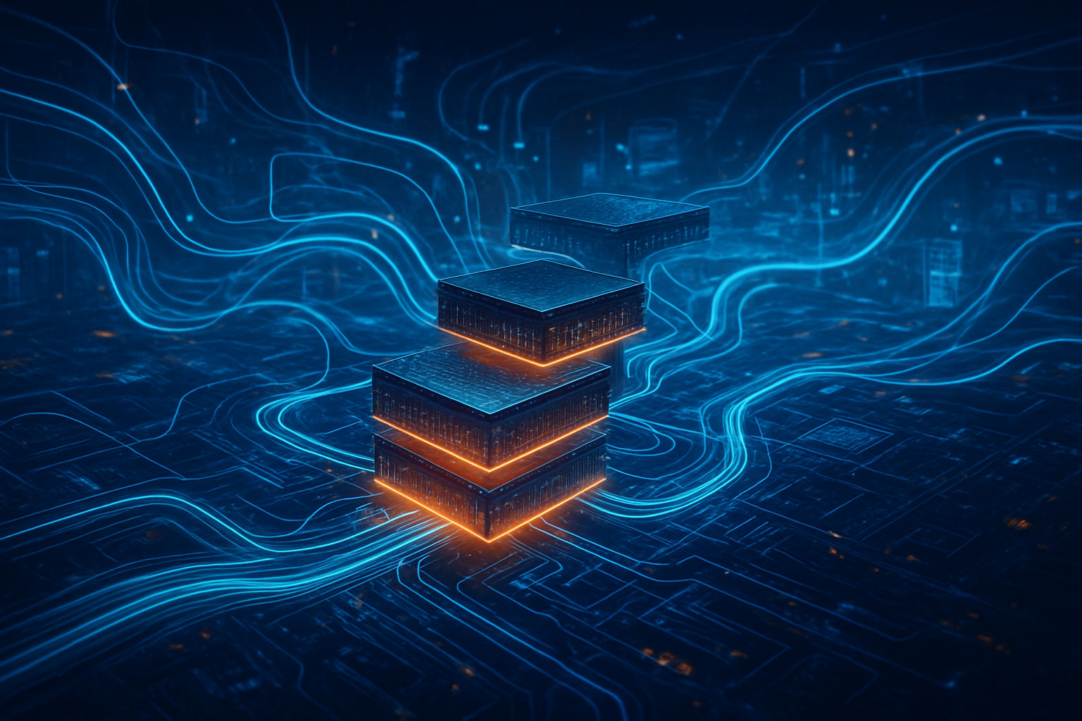
The Technical Evolution: HBM, LPDDR6, 3D DRAM, and CXL Drive AI Forward
The technical evolution of DRAM and NAND Flash memory is rapidly accelerating to overcome the "memory wall"—the performance gap between processors and traditional memory—which is a major bottleneck for AI workloads. Innovations are focused on higher bandwidth, greater capacity, and improved power efficiency, transforming memory into a central pillar of AI hardware design.
High-Bandwidth Memory (HBM) remains critical, with HBM3 and HBM3E as current standards and HBM4 anticipated by late 2025. HBM4 is projected to achieve speeds of 10+ Gbps, double the channel count per stack, and offer a significant 40% improvement in power efficiency over HBM3. Its stacked architecture, utilizing Through-Silicon Vias (TSVs) and advanced packaging, is indispensable for AI accelerators like those from NVIDIA (NASDAQ: NVDA) and AMD (NASDAQ: AMD), which require rapid transfer of large data volumes for training large language models (LLMs). Beyond HBM, the concept of 3D DRAM is evolving to integrate processing capabilities directly within the memory. Startups like NEO Semiconductor are developing "3D X-AI" technology, proposing 3D-stacked DRAM with integrated neuron circuitry that could boost AI performance by up to 100 times and increase memory density by 8 times compared to current HBM, while dramatically cutting power consumption by 99%.
For power-efficient AI, particularly at the edge, the newly published JEDEC LPDDR6 standard is a game-changer. Elevating per-bit speed to 14.4 Gbps and expanding the data width, LPDDR6 delivers a total bandwidth of 691 Gb/s—twice that of LPDDR5X. This makes it ideal for AI inference models and edge workloads that require reduced latency and improved throughput with irregular, high-frequency access patterns. Cadence Design Systems (NASDAQ: CDNS) has already announced LPDDR6/5X memory IP achieving these breakthrough speeds. Meanwhile, Compute Express Link (CXL) is emerging as a transformative interface standard. CXL allows systems to expand memory capacity, pool and share memory dynamically across CPUs, GPUs, and accelerators, and ensures cache coherency, significantly improving memory utilization and efficiency for AI. Wolley Inc., for example, introduced a CXL memory expansion controller at FMS2025 that provides both memory and storage interfaces simultaneously over shared PCIe ports, boosting bandwidth and reducing total cost of ownership for running LLM inference.
In the realm of storage, NAND Flash memory is also undergoing significant advancements. Manufacturers continue to scale 3D NAND with more layers, with Samsung (KRX: 005930) beginning mass production of its 9th-generation QLC V-NAND. Quad-Level Cell (QLC) NAND, with its higher storage density and lower cost, is increasingly adopted in enterprise SSDs for AI inference, where read operations dominate. SK Hynix (KRX: 000660) has announced mass production of the world's first 321-layer 2Tb QLC NAND flash, scheduled to enter the AI data center market in the first half of 2026. Furthermore, SanDisk (NASDAQ: SNDK) and SK Hynix are collaborating to co-develop High Bandwidth Flash (HBF), which integrates HBM-like concepts with NAND-based technology, aiming to provide a denser memory tier with 8-16 times more memory in the same footprint as HBM, with initial samples expected in late 2026. Industry experts widely acknowledge these advancements as critical for overcoming the "memory wall" and enabling the next generation of powerful, energy-efficient AI hardware, despite significant challenges related to power consumption and infrastructure costs.
Reshaping the AI Industry: Beneficiaries, Battles, and Breakthroughs
The dynamic trends in DRAM and NAND Flash memory are fundamentally reshaping the competitive landscape for AI companies, tech giants, and startups, creating significant beneficiaries, intensifying competitive battles, and driving strategic shifts. The overarching theme is that memory is no longer a commodity but a strategic asset, dictating the performance and efficiency of AI systems.
Memory providers like SK Hynix (KRX: 000660), Samsung (KRX: 005930), and Micron Technology (NASDAQ: MU) are the primary beneficiaries of this AI-driven memory boom. Their strategic shift towards HBM production, significant R&D investments in HBM4, 3D DRAM, and LPDDR6, and advanced packaging techniques are crucial for maintaining leadership. SK Hynix, in particular, has emerged as a dominant force in HBM, with Micron's HBM capacity for 2025 and much of 2026 already sold out. These companies have become crucial partners in the AI hardware supply chain, gaining increased influence on product development, pricing, and competitive positioning. Hyperscalers such as Google (NASDAQ: GOOGL), Microsoft (NASDAQ: MSFT), Meta Platforms (NASDAQ: META), and Amazon (NASDAQ: AMZN), who are at the forefront of AI infrastructure build-outs, are driving massive demand for advanced memory. They are strategically investing in developing their own custom silicon, like Google's TPUs and Amazon's Trainium, to optimize performance and integrate memory solutions tightly with their AI software stacks, actively deploying CXL for memory pooling and exploring QLC NAND for cost-effective, high-capacity data storage.
The competitive implications are profound. AI chip designers like NVIDIA (NASDAQ: NVDA), AMD (NASDAQ: AMD), and Intel (NASDAQ: INTC) are heavily reliant on advanced HBM for their AI accelerators. Their ability to deliver high-performance chips with integrated or tightly coupled advanced memory is a key competitive differentiator. NVIDIA's upcoming Blackwell GPUs, for instance, will heavily leverage HBM4. The emergence of CXL is enabling a shift towards memory-centric and composable architectures, allowing for greater flexibility, scalability, and cost efficiency in AI data centers, disrupting traditional server designs and favoring vendors who can offer CXL-enabled solutions like GIGABYTE Technology (TPE: 2376). For AI startups, while the demand for specialized AI chips and novel architectures presents opportunities, access to cutting-edge memory technologies like HBM can be a challenge due to high demand and pre-orders by larger players. Managing the increasing cost of advanced memory and storage is also a crucial factor for their financial viability and scalability, making strategic partnerships with memory providers or cloud giants offering advanced memory infrastructure critical for success.
The potential for disruption is significant. The proposed mass production of 3D DRAM with integrated AI processing, offering immense density and performance gains, could fundamentally redefine the memory landscape, potentially displacing HBM as the leading high-performance memory solution for AI in the longer term. Similarly, QLC NAND's cost-effectiveness for large datasets, coupled with its performance suitability for read-heavy AI inference, positions it as a disruptive force against traditional HDDs and even some TLC-based SSDs in AI storage. Strategic partnerships, such as OpenAI's collaborations with Samsung and SK Hynix for its "Stargate" project, are becoming crucial for securing supply and co-developing next-generation memory solutions tailored for specific AI workloads.
Wider Significance: Powering the AI Revolution with Caution
The advancements in DRAM and NAND Flash memory technologies are fundamentally reshaping the broader Artificial Intelligence (AI) landscape, enabling more powerful, efficient, and sophisticated AI systems across various applications, from large-scale data centers to pervasive edge devices. These innovations are critical in overcoming the "memory wall" and fueling the AI revolution, but they also introduce new concerns and significant societal impacts.
The ability of HBM to feed data to powerful AI accelerators, LPDDR6's role in enabling efficient edge AI, 3D DRAM's potential for in-memory processing, and CXL's capacity for memory pooling are all crucial for the next generation of AI. QLC NAND's cost-effectiveness for storing massive AI datasets complements these high-performance memory solutions. This fits into the broader AI landscape by providing the foundational hardware necessary for scaling large language models, enabling real-time AI inference, and expanding AI capabilities to power-constrained environments. The increased memory bandwidth and capacity are directly enabling the development of more complex and context-aware AI systems.
However, these advancements also bring forth a range of potential concerns. As AI systems gain "near-infinite memory" and can retain detailed information about user interactions, concerns about data privacy intensify. If AI is trained on biased data, its enhanced memory can amplify these biases, leading to erroneous decision-making and perpetuating societal inequalities. An over-reliance on AI's perfect memory could also lead to "cognitive offloading" in humans, potentially diminishing human creativity and critical thinking. Furthermore, the explosive growth of AI applications and the demand for high-performance memory significantly increase power consumption in data centers, posing challenges for sustainable AI computing and potentially leading to energy crises. Google (NASDAQ: GOOGL)'s data center power usage increased by 27% in 2024, predominantly due to AI workloads, underscoring this urgency.
Comparing these developments to previous AI milestones reveals a recurring theme: advancements in computational power and memory capacity have always been critical enablers. The stored-program architecture of early computing, the development of neural networks, the advent of GPU acceleration, and the breakthrough of the transformer architecture for LLMs all demanded corresponding improvements in memory. Today's HBM, LPDDR6, 3D DRAM, CXL, and QLC NAND represent the latest iteration of this symbiotic relationship, providing the necessary infrastructure to power the next generation of AI, particularly for context-aware and "agentic" AI systems that require unprecedented memory capacity, bandwidth, and efficiency. The long-term societal impacts include enhanced personalization, breakthroughs in various industries, and new forms of human-AI interaction, but these must be balanced with careful consideration of ethical implications and sustainable development.
The Horizon: What Comes Next for AI Memory
The future of AI memory technology is poised for continuous and rapid evolution, driven by the relentless demands of increasingly sophisticated AI workloads. Experts predict a landscape of ongoing innovation, expanding applications, and persistent challenges that will necessitate a fundamental rethinking of traditional memory architectures.
In the near term, the evolution of HBM will continue to dominate the high-performance memory segment. HBM4, expected by late 2025, will push boundaries with higher capacities (up to 64 GB per stack) and a significant 40% improvement in power efficiency over HBM3. Manufacturers are also exploring advanced packaging technologies like copper-copper hybrid bonding for HBM4 and beyond, promising even greater performance. For power-efficient AI, LPDDR6 will solidify its role in edge AI, automotive, and client computing, with further enhancements in speed and power efficiency. Beyond traditional DRAM, the development of Compute-in-Memory (CIM) and Processing-in-Memory (PIM) architectures will gain momentum, aiming to integrate computing logic directly within memory arrays to drastically reduce data movement bottlenecks and improve energy efficiency for AI. In NAND Flash, the aggressive scaling of 3D NAND to 300+ layers and eventually 1,000+ layers by the end of the decade is expected, along with the continued adoption of QLC and the emergence of Penta-Level Cell (PLC) NAND for even higher density. A significant development to watch for is High Bandwidth Flash (HBF), co-developed by SanDisk (NASDAQ: SNDK) and SK Hynix (KRX: 000660), which integrates HBM-like concepts with NAND-based technology, promising a new memory tier with 8-16 times more capacity than HBM in the same footprint as HBM, with initial samples expected in late 2026.
Potential applications on the horizon are vast. AI servers and hyperscale data centers will continue to be the primary drivers, demanding massive quantities of HBM for training and inference, and high-density, high-performance NVMe SSDs for data lakes. OpenAI's "Stargate" project, for instance, is projected to require an unprecedented amount of HBM chips. The advent of "AI PCs" and AI-enabled smartphones will also drive significant demand for high-speed, high-capacity, and low-power DRAM and NAND to enable on-device generative AI and faster local processing. Edge AI and IoT devices will increasingly rely on energy-efficient, high-density, and low-latency memory solutions for real-time decision-making in autonomous vehicles, robotics, and industrial control.
However, several challenges need to be addressed. The "memory wall" remains a persistent bottleneck, and the power consumption of DRAM, especially in data centers, is a major concern for sustainable AI. Scaling traditional 2D DRAM is facing physical and process limits, while 3D NAND manufacturing complexities, including High Aspect Ratio (HAR) etching and yield issues, are growing. The cost premiums associated with high-performance memory solutions like HBM also pose a challenge. Experts predict an "insatiable appetite" for memory from AI data centers, consuming the majority of global memory and flash production capacity, leading to widespread shortages and significant price surges for both DRAM and NAND Flash, potentially lasting a decade. The memory market is forecast to reach nearly $300 billion by 2027, with AI-related applications accounting for 53% of the DRAM market's total addressable market (TAM) by that time. The industry is moving towards system-level optimization, including advanced packaging and interconnects like CXL, and a fundamental shift towards memory-centric computing, where memory is not just a supporting component but a central driver of AI performance and efficiency.
Comprehensive Wrap-up: Memory's Central Role in the AI Era
The memory chip market, encompassing DRAM and NAND Flash, stands at a pivotal juncture, fundamentally reshaped by the unprecedented demands of the Artificial Intelligence industry. As of October 2025, the key takeaway is clear: memory is no longer a peripheral component but a strategic imperative, driving an "AI supercycle" that is redefining market dynamics and accelerating technological innovation.
This development's significance in AI history is profound. High-Bandwidth Memory (HBM) has emerged as the single most critical component, experiencing explosive growth and compelling major manufacturers like Samsung (KRX: 005930), SK Hynix (KRX: 000660), and Micron Technology (NASDAQ: MU) to prioritize its production. This shift, coupled with robust demand for high-capacity NAND Flash in enterprise SSDs, has led to soaring memory prices and looming supply shortages, a trend some experts predict could persist for a decade. The technical advancements—from HBM4 and LPDDR6 to 3D DRAM with integrated processing and the transformative Compute Express Link (CXL) standard—are directly addressing the "memory wall," enabling larger, more complex AI models and pushing the boundaries of what AI can achieve.
Our final thoughts on the long-term impact point to a sustained transformation rather than a cyclical fluctuation. The "AI supercycle" is structural, making memory a competitive differentiator in the crowded AI landscape. Systems with robust, high-bandwidth memory will enable more adaptable, energy-efficient, and versatile AI, leading to breakthroughs in personalized medicine, predictive maintenance, and entirely new forms of human-AI interaction. However, this future also brings challenges, including intensified concerns about data privacy, the potential for cognitive offloading, and the escalating energy consumption of AI data centers. The ethical implications of AI with "infinite memory" will necessitate robust frameworks for transparency and accountability.
In the coming weeks and months, several critical areas warrant close observation. Keep a keen eye on the continued development and adoption of HBM4, particularly its integration into next-generation AI accelerators. Monitor the trajectory of memory pricing, as recent hikes suggest elevated costs will persist into 2026. Watch how major memory suppliers continue to adjust their production mix towards HBM, as any significant shifts could impact the supply of mainstream DRAM and NAND. Furthermore, observe advancements in next-generation NAND technology, especially 3D NAND scaling and High Bandwidth Flash (HBF), which will be crucial for meeting the increasing demand for high-capacity SSDs in AI data centers. Finally, the momentum of Edge AI in PCs and smartphones, and the massive memory consumption of projects like OpenAI's "Stargate," will be key indicators of the AI industry's continued impact on the memory market.
This content is intended for informational purposes only and represents analysis of current AI developments.
TokenRing AI delivers enterprise-grade solutions for multi-agent AI workflow orchestration, AI-powered development tools, and seamless remote collaboration platforms. For more information, visit https://www.tokenring.ai/.