Tag: 3D Stacking

  • Advanced Packaging: The Unsung Hero Propelling AI’s Next Revolution

    Advanced Packaging: The Unsung Hero Propelling AI’s Next Revolution

    In an era where Artificial Intelligence (AI) is rapidly redefining industries and daily life, the relentless pursuit of faster, more efficient, and more powerful computing hardware has become paramount. While much attention focuses on groundbreaking algorithms and software innovations, a quieter revolution is unfolding beneath the surface of every cutting-edge AI chip: advanced semiconductor packaging. Technologies like 3D stacking, chiplets, and fan-out packaging are no longer mere afterthoughts in chip manufacturing; they are the critical enablers boosting the performance, power efficiency, and cost-effectiveness of semiconductors, fundamentally shaping the future of high-performance computing (HPC) and AI hardware.

    These innovations are steering the semiconductor industry beyond the traditional confines of 2D integration, where components are laid out side-by-side on a single plane. As Moore's Law—the decades-old prediction that the number of transistors on a microchip doubles approximately every two years—faces increasing physical and economic limitations, advanced packaging has emerged as the essential pathway to continued performance scaling. By intelligently integrating and interconnecting components in three dimensions and modular forms, these technologies are unlocking unprecedented capabilities, allowing AI models to grow in complexity and speed, from the largest data centers to the smallest edge devices.

    Beyond the Monolith: Technical Innovations Driving AI Hardware

    The shift to advanced packaging marks a profound departure from the monolithic chip design of the past, introducing intricate architectures that maximize data throughput and minimize latency.

    3D Stacking (3D ICs)

    3D stacking involves vertically integrating multiple semiconductor dies (chips) within a single package, interconnected by ultra-short, high-bandwidth connections. The most prominent of these are Through-Silicon Vias (TSVs), which are vertical electrical connections passing directly through the silicon layers, or advanced copper-to-copper (Cu-Cu) hybrid bonding, which creates molecular-level connections. This vertical integration dramatically reduces the physical distance data must travel, leading to significantly faster data transfer speeds, improved performance, and enhanced power efficiency due to shorter interconnects and lower capacitance. For AI, 3D ICs can offer I/O density increases of up to 100x and energy-per-bit transfer reductions of up to 30x. This is particularly crucial for High Bandwidth Memory (HBM), which utilizes 3D stacking with TSVs to achieve unprecedented memory bandwidth, a vital component for data-intensive AI workloads. The AI research community widely acknowledges 3D stacking as indispensable for overcoming the "memory wall" bottleneck, providing the necessary bandwidth and low latency for complex machine learning models.

    Chiplets

    Chiplets represent a modular approach, breaking down a large, complex chip into smaller, specialized dies, each performing a specific function (e.g., CPU, GPU, memory, I/O, AI accelerator). These pre-designed and pre-tested chiplets are then interconnected within a single package, often using 2.5D integration where they are mounted side-by-side on a silicon interposer, or even 3D integration. This modularity offers several advantages over traditional monolithic System-on-Chip (SoC) designs: improved manufacturing yields (as defects on smaller chiplets are less costly), greater design flexibility, and the ability to mix and match components from various process nodes to optimize for performance, power, and cost. Standards like the Universal Chiplet Interconnect Express (UCIe) are emerging to facilitate interoperability between chiplets from different vendors. Industry experts view chiplets as redefining the future of AI processing, providing a scalable and customizable approach essential for generative AI, high-performance computing, and edge AI systems.

    Fan-Out Packaging (FOWLP/FOPLP)

    Fan-out Wafer-Level Packaging (FOWLP) is an advanced technique where the connection points (I/Os) are redistributed from the chip's periphery over a larger area, extending beyond the original die footprint. After dicing, individual dies are repositioned on a carrier wafer or panel, molded, and then connected via Redistribution Layers (RDLs) and solder balls. This substrateless or substrate-light design enables ultra-thin and compact packages, often reducing package size by 40%, while supporting a higher number of I/Os. FOWLP also offers improved thermal and electrical performance due to shorter electrical paths and better heat spreading. Panel-Level Packaging (FOPLP) further enhances cost-efficiency by processing on larger, square panels instead of round wafers. FOWLP is recognized as a game-changer, providing high-density packaging and excellent performance for applications in 5G, automotive, AI, and consumer electronics, as exemplified by Apple's (NASDAQ: AAPL) use of TSMC's (NYSE: TSM) Integrated Fan-Out (InFO) technology in its A-series chips.

    Reshaping the AI Competitive Landscape

    The strategic importance of advanced packaging is profoundly impacting AI companies, tech giants, and startups, creating new competitive dynamics and strategic advantages.

    Major tech giants are at the forefront of this transformation. NVIDIA (NASDAQ: NVDA), a leader in AI accelerators, heavily relies on advanced packaging, particularly TSMC's CoWoS (Chip-on-Wafer-on-Substrate) technology, for its high-performance GPUs like the Hopper H100 and upcoming Blackwell chips. NVIDIA's transition to CoWoS-L technology signifies the continuous demand for enhanced design and packaging flexibility for large AI chips. Intel (NASDAQ: INTC) is aggressively developing its own advanced packaging solutions, including Foveros (3D stacking) and EMIB (Embedded Multi-die Interconnect Bridge, a 2.5D technology). Intel's EMIB is gaining traction, with cloud service providers (CSPs) like Alphabet (NASDAQ: GOOGL) evaluating it for their custom AI accelerators (TPUs), driven by strong demand and a need for diversified packaging supply. This collaboration with partners like Amkor Technology (NASDAQ: AMKR) to scale EMIB production highlights the strategic importance of packaging expertise.

    Advanced Micro Devices (NASDAQ: AMD) has been a pioneer in chiplet-based CPUs and GPUs with its EPYC and Instinct lines, leveraging its Infinity Fabric interconnect, and is pushing 3D stacking with its 3D V-Cache technology. Samsung Electronics (KRX: 005930), a major player in memory, foundry, and packaging, offers its X-Cube technology for vertical stacking of logic and SRAM dies, presenting a strategic advantage with its integrated turnkey solutions.

    For AI startups, advanced packaging presents both opportunities and challenges. Chiplets, in particular, can lower entry barriers by reducing the need to design complex monolithic chips from scratch, allowing startups to integrate best-in-class IP and accelerate time-to-market with specialized AI accelerators. Companies like Mixx Technologies are innovating with optical interconnect systems using silicon photonics and advanced packaging. However, startups face challenges such as the high manufacturing complexity and cost of advanced packaging, thermal management issues, and the need for skilled labor.

    The competitive landscape is shifting, with packaging no longer a commodity but a strategic differentiator. Companies with strong access to advanced foundries (like TSMC and Intel Foundry) and packaging expertise gain a significant edge. Outsourced Semiconductor Assembly and Test (OSAT) vendors like Amkor Technology are becoming critical partners. The capacity crunch for leading advanced packaging technologies is prompting tech giants to diversify their supply chains, fostering competition and innovation. This evolution blurs traditional roles, with back-end design and packaging gaining immense value, pushing the industry towards system-level co-optimization. This disruption to traditional monolithic chip designs means that purely monolithic high-performance AI chips may become less competitive as multi-chip integration offers superior performance and cost efficiencies.

    A New Era for AI: Wider Significance and Future Implications

    Advanced packaging technologies represent a fundamental hardware-centric breakthrough for AI, akin to the advent of Graphics Processing Units (GPUs) in the mid-2000s, which provided the parallel processing power to catalyze the deep learning revolution. Just as GPUs enabled the training of previously intractable neural networks, advanced packaging provides the essential physical infrastructure to realize and deploy today's and tomorrow's sophisticated AI models at scale. It directly addresses the "memory wall" and other fundamental hardware bottlenecks, pushing past the limits of traditional silicon scaling into the "More than Moore" era, where performance gains are achieved through innovative integration.

    The overall impact on the AI landscape is profound: enhanced performance, improved power efficiency, miniaturization for edge AI, and unparalleled scalability and flexibility through chiplets. These advancements are crucial for handling the immense computational demands of Large Language Models (LLMs) and generative AI, enabling larger and more complex AI models.

    However, this transformation is not without its challenges. The increased power density from tightly integrated components exacerbates thermal management issues, demanding innovative cooling solutions. Manufacturing complexity, especially with hybrid bonding, increases the risk of defects and complicates yield management. Testing heterogeneous chiplet-based systems is also significantly more complex than monolithic chips, requiring robust testing protocols. The absence of universal chiplet testing standards and interoperability protocols also presents a challenge, though initiatives like UCIe are working to address this. Furthermore, the high capital investment for advanced packaging equipment and expertise can be substantial, and supply chain constraints, such as TSMC's advanced packaging capacity, remain a concern.

    Looking ahead, experts predict a dynamic future for advanced packaging, with AI at its core. Near-term advancements (1-5 years) include the widespread adoption of hybrid bonding for finer interconnect pitches, continued evolution of HBM with higher stacks, and improved TSV fabrication. Chiplets will see standardized interfaces and increasingly specialized AI chiplets, while fan-out packaging will move towards higher density, Panel-Level Packaging (FOPLP), and integration with glass substrates for enhanced thermal stability.

    Long-term (beyond 5 years), the industry anticipates logic-memory hybrids becoming mainstream, ultra-dense 3D stacks, active interposers with embedded transistors, and a transition to 3.5D packaging. Chiplets are expected to lead to fully modular semiconductor designs, with AI itself playing a pivotal role in optimizing chiplet-based design automation. Co-Packaged Optics (CPO), integrating optical engines directly adjacent to compute dies, will drastically improve interconnect bandwidth and reduce power consumption, with significant adoption expected by the late 2020s in AI accelerators.

    The Foundation of AI's Future

    In summary, advanced semiconductor packaging technologies are no longer a secondary consideration but a fundamental driver of innovation, performance, and efficiency for the demanding AI landscape. By moving beyond traditional 2D integration, these innovations are directly addressing the core hardware limitations that could otherwise impede AI's progress. The relentless pursuit of denser, faster, and more power-efficient chip architectures through 3D stacking, chiplets, and fan-out packaging is critical for unlocking the full potential of AI across all sectors, from cloud-based supercomputing to embedded edge devices.

    The coming weeks and months will undoubtedly bring further announcements and breakthroughs in advanced packaging, as companies continue to invest heavily in this crucial area. We can expect to see continued advancements in hybrid bonding, the proliferation of standardized chiplet interfaces, and further integration of optical interconnects, all contributing to an even more powerful and pervasive AI future. The race to build the most efficient and powerful AI hardware is far from over, and advanced packaging is leading the charge.


    This content is intended for informational purposes only and represents analysis of current AI developments.

    TokenRing AI delivers enterprise-grade solutions for multi-agent AI workflow orchestration, AI-powered development tools, and seamless remote collaboration platforms.
    For more information, visit https://www.tokenring.ai/.

  • The Dawn of a New Era: AI Chips Break Free From Silicon’s Chains

    The Dawn of a New Era: AI Chips Break Free From Silicon’s Chains

    The relentless march of artificial intelligence, with its insatiable demand for computational power and energy efficiency, is pushing the foundational material of the digital age, silicon, to its inherent physical limits. As traditional silicon-based semiconductors encounter bottlenecks in performance, heat dissipation, and power consumption, a profound revolution is underway. Researchers and industry leaders are now looking to a new generation of exotic materials and groundbreaking architectures to redefine AI chip design, promising unprecedented capabilities and a future where AI's potential is no longer constrained by a single element.

    This fundamental shift is not merely an incremental upgrade but a foundational re-imagining of how AI hardware is built, with immediate and far-reaching implications for the entire technology landscape. The goal is to achieve significantly faster processing speeds, dramatically lower power consumption crucial for large language models and edge devices, and denser, more compact chips. This new era of materials and architectures will unlock advanced AI capabilities across various autonomous systems, industrial automation, healthcare, and smart cities.

    Redefining Performance: Technical Deep Dive into Beyond-Silicon Innovations

    The landscape of AI semiconductor design is rapidly evolving beyond traditional silicon-based architectures, driven by the escalating demands for higher performance, energy efficiency, and novel computational paradigms. Emerging materials and architectures promise to revolutionize AI hardware by overcoming the physical limitations of silicon, enabling breakthroughs in speed, power consumption, and functional integration.

    Carbon Nanotubes (CNTs)

    Carbon Nanotubes are cylindrical structures made of carbon atoms arranged in a hexagonal lattice, offering superior electrical conductivity, exceptional stability, and an ultra-thin structure. They enable electrons to flow with minimal resistance, significantly reducing power consumption and increasing processing speeds compared to silicon. For instance, a CNT-based Tensor Processing Unit (TPU) has achieved 88% accuracy in image recognition with a mere 295 μW, demonstrating nearly 1,700 times more efficiency than Google's (NASDAQ: GOOGL) silicon TPU. Some CNT chips even employ ternary logic systems, processing data in a third state (beyond binary 0s and 1s) for faster, more energy-efficient computation. This allows CNT processors to run up to three times faster while consuming about one-third of the energy of silicon predecessors. The AI research community has hailed CNT-based AI chips as an "enormous breakthrough," potentially accelerating the path to artificial general intelligence (AGI) due to their energy efficiency.

    2D Materials (Graphene, MoS2)

    Atomically thin crystals like Graphene and Molybdenum Disulfide (MoS₂) offer unique quantum mechanical properties. Graphene, a single layer of carbon, boasts electron movement 100 times faster than silicon and superior thermal conductivity (~5000 W/m·K), enabling ultra-fast processing and efficient heat dissipation. While graphene's lack of a natural bandgap presents a challenge for traditional transistor switching, MoS₂ naturally possesses a bandgap, making it more suitable for direct transistor fabrication. These materials promise ultimate scaling limits, paving the way for flexible electronics and a potential 50% reduction in power consumption compared to silicon's projected performance. Experts are excited about their potential for more efficient AI accelerators and denser memory, actively working on hybrid approaches that combine 2D materials with silicon to enhance performance.

    Neuromorphic Computing

    Inspired by the human brain, neuromorphic computing aims to mimic biological neural networks by integrating processing and memory. These systems, comprising artificial neurons and synapses, utilize spiking neural networks (SNNs) for event-driven, parallel processing. This design fundamentally differs from the traditional von Neumann architecture, which separates CPU and memory, leading to the "memory wall" bottleneck. Neuromorphic chips like IBM's (NYSE: IBM) TrueNorth and Intel's (NASDAQ: INTC) Loihi are designed for ultra-energy-efficient, real-time learning and adaptation, consuming power only when neurons are triggered. This makes them significantly more efficient, especially for edge AI applications where low power and real-time decision-making are crucial, and is seen as a "compelling answer" to the massive energy consumption of traditional AI models.

    3D Stacking (3D-IC)

    3D stacking involves vertically integrating multiple chip dies, interconnected by Through-Silicon Vias (TSVs) and advanced techniques like hybrid bonding. This method dramatically increases chip density, reduces interconnect lengths, and significantly boosts bandwidth and energy efficiency. It enables heterogeneous integration, allowing logic, memory (e.g., High-Bandwidth Memory – HBM), and even photonics to be stacked within a single package. This "ranch house into a high-rise" approach for transistors significantly reduces latency and power consumption—up to 1/7th compared to 2D designs—which is critical for data-intensive AI workloads. The AI research community is "overwhelmingly optimistic," viewing 3D stacking as the "backbone of innovation" for the semiconductor sector, with companies like TSMC (NYSE: TSM) and Intel (NASDAQ: INTC) leading in advanced packaging.

    Spintronics

    Spintronics leverages the intrinsic quantum property of electrons called "spin" (in addition to their charge) for information processing and storage. Unlike conventional electronics that rely solely on electron charge, spintronics manipulates both charge and spin states, offering non-volatile memory (e.g., MRAM) that retains data without power. This leads to significant energy efficiency advantages, as spintronic memory can consume 60-70% less power during write operations and nearly 90% less in standby modes compared to DRAM. Spintronic devices also promise faster switching speeds and higher integration density. Experts see spintronics as a "breakthrough" technology capable of slashing processor power by 80% and enabling neuromorphic AI hardware by 2030, marking the "dawn of a new era" for energy-efficient computing.

    Shifting Sands: Competitive Implications for the AI Industry

    The shift beyond traditional silicon semiconductors represents a monumental milestone for the AI industry, promising significant competitive shifts and potential disruptions. Companies that master these new materials and architectures stand to gain substantial strategic advantages.

    Major tech giants are heavily invested in these next-generation technologies. Intel (NASDAQ: INTC) and IBM (NYSE: IBM) are leading the charge in neuromorphic computing with their Loihi and NorthPole chips, respectively, aiming to outperform conventional CPU/GPU systems in energy efficiency for AI inference. This directly challenges NVIDIA's (NASDAQ: NVDA) GPU dominance in certain AI processing areas, especially as companies seek more specialized and efficient hardware. Qualcomm (NASDAQ: QCOM), Samsung (KRX: 005930), and NXP Semiconductors (NASDAQ: NXPI) are also active in the neuromorphic space, particularly for edge AI applications.

    In 3D stacking, TSMC (NYSE: TSM) with its 3DFabric and Samsung (KRX: 005930) with its SAINT platform are fiercely competing to provide advanced packaging solutions for AI accelerators and large language models. NVIDIA (NASDAQ: NVDA) itself is exploring 3D stacking of GPU tiers and silicon photonics for its future AI accelerators, with predicted implementations between 2028-2030. These advancements enable companies to create "mini-chip systems" that offer significant advantages over monolithic dies, disrupting traditional chip design and manufacturing.

    For novel materials like Carbon Nanotubes and 2D materials, IBM (NYSE: IBM) and Intel (NASDAQ: INTC) are investing in fundamental materials science, seeking to integrate these into next-generation computing platforms. Google DeepMind (NASDAQ: GOOGL) is even leveraging AI to discover new 2D materials, gaining a first-mover advantage in material innovation. Companies that successfully commercialize CNT-based AI chips could establish new industry standards for energy efficiency, especially for edge AI.

    Spintronics, with its promise of non-volatile, energy-efficient memory, sees investment from IBM (NYSE: IBM), Intel (NASDAQ: INTC), and Samsung (KRX: 005930), which are developing MRAM solutions and exploring spin-based logic devices. Startups like Everspin Technologies (NASDAQ: MRAM) are key players in specialized MRAM solutions. This could disrupt traditional volatile memory solutions (DRAM, SRAM) in AI applications where non-volatility and efficiency are critical, potentially reducing the energy footprint of large data centers.

    Overall, companies with robust R&D in these areas and strong ecosystem support will secure leading market positions. Strategic partnerships between foundries, EDA tool providers (like Ansys (NASDAQ: ANSS) and Synopsys (NASDAQ: SNPS)), and chip designers are becoming crucial for accelerating innovation and navigating this evolving landscape.

    A New Chapter for AI: Broader Implications and Challenges

    The advancements in semiconductor materials and architectures beyond traditional silicon are not merely technical feats; they represent a fundamental re-imagining of computing itself, poised to redefine AI capabilities, drive greater efficiency, and expand AI's reach into unprecedented territories. This "hardware renaissance" is fundamentally reshaping the AI landscape by enabling the "AI Supercycle" and addressing critical needs.

    These developments are fueling the insatiable demand for high-performance computing (HPC) and large language models (LLMs), which require advanced process nodes (down to 2nm) and sophisticated packaging. The unprecedented demand for High-Bandwidth Memory (HBM), surging by 150% in 2023 and over 200% in 2024, is a direct consequence of data-intensive AI systems. Furthermore, beyond-silicon materials are crucial for enabling powerful and energy-efficient AI chips at the edge, where power budgets are tight and real-time processing is essential for autonomous vehicles, IoT devices, and wearables. This also contributes to sustainable AI by addressing the substantial and growing electricity consumption of global computing infrastructure.

    The impacts are transformative: unprecedented speed, lower latency, and significantly reduced power consumption by minimizing the "von Neumann bottleneck" and "memory wall." This enables new AI capabilities previously unattainable with silicon, such as molecular-level modeling for faster drug discovery, real-time decision-making for autonomous systems, and enhanced natural language processing. Moreover, materials like diamond and gallium oxide (Ga₂O₃) can enable AI systems to operate in harsh industrial or even space environments, expanding AI applications into new frontiers.

    However, this revolution is not without its concerns. Manufacturing cutting-edge AI chips is incredibly complex and resource-intensive, requiring completely new transistor architectures and fabrication techniques that are not yet commercially viable or scalable. The cost of building advanced semiconductor fabs can reach up to $20 billion, with each new generation demanding more sophisticated and expensive equipment. The nascent supply chains for exotic materials could initially limit widespread adoption, and the industry faces talent shortages in critical areas. Integrating new materials and architectures, especially in hybrid systems combining electronic and photonic components, presents complex engineering challenges.

    Despite these hurdles, the advancements are considered a "revolutionary leap" and a "monumental milestone" in AI history. Unlike previous AI milestones that were primarily algorithmic or software-driven, this hardware-driven revolution will unlock "unprecedented territories" for AI applications, enabling systems that are faster, more energy-efficient, capable of operating in diverse and extreme conditions, and ultimately, more intelligent. It directly addresses the unsustainable energy demands of current AI, paving the way for more environmentally sustainable and scalable AI deployments globally.

    The Horizon: Envisioning Future AI Semiconductor Developments

    The journey beyond silicon is set to unfold with a series of transformative developments in both materials and architectures, promising to unlock even greater potential for artificial intelligence.

    In the near-term (1-5 years), we can expect to see continued integration and adoption of Gallium Nitride (GaN) and Silicon Carbide (SiC) in power electronics, 5G infrastructure, and AI acceleration, offering faster switching and reduced power loss. 2D materials like graphene and MoS₂ will see significant advancements in monolithic 3D integration, leading to reduced processing time, power consumption, and latency for AI computing, with some projections indicating up to a 50% reduction in power consumption compared to silicon by 2037. Ferroelectric materials will gain traction for non-volatile memory and neuromorphic computing, addressing the "memory bottleneck" in AI. Architecturally, neuromorphic computing will continue its ascent, with chips like IBM's North Pole leading the charge in energy-efficient, brain-inspired AI. In-Memory Computing (IMC) / Processing-in-Memory (PIM), utilizing technologies like RRAM and PCM, will become more prevalent to reduce data transfer bottlenecks. 3D chiplets and advanced packaging will become standard for high-performance AI, enabling modular designs and closer integration of compute and memory. Silicon photonics will enhance on-chip communication for faster, more efficient AI chips in data centers.

    Looking further into the long-term (5+ years), Ultra-Wide Bandgap (UWBG) semiconductors such as diamond and gallium oxide (Ga₂O₃) could enable AI systems to operate in extremely harsh environments, from industrial settings to space. The vision of fully integrated 2D material chips will advance, leading to unprecedented compactness and efficiency. Superconductors are being explored for groundbreaking applications in quantum computing and ultra-low-power edge AI devices. Architecturally, analog AI will gain traction for its potential energy efficiency in specific workloads, and we will see increased progress in hybrid quantum-classical architectures, where quantum computing integrates with semiconductors to tackle complex AI algorithms beyond classical capabilities.

    These advancements will enable a wide array of transformative AI applications, from more efficient high-performance computing (HPC) and data centers powering generative AI, to smaller, more powerful, and energy-efficient edge AI and IoT devices (wearables, smart sensors, robotics, autonomous vehicles). They will revolutionize electric vehicles (EVs), industrial automation, and 5G/6G networks. Furthermore, specialized AI accelerators will be purpose-built for tasks like natural language processing and computer vision, and the ability to operate in harsh environments will expand AI's reach into new frontiers like medical implants and advanced scientific discovery.

    However, challenges remain. The cost and scalability of manufacturing new materials, integrating them into existing CMOS technology, and ensuring long-term reliability are significant hurdles. Heat dissipation and energy efficiency, despite improvements, will remain persistent challenges as transistor densities increase. Experts predict a future of hybrid chips incorporating novel materials alongside silicon, and a paradigm shift towards AI-first semiconductor architectures built from the ground up for AI workloads. AI itself will act as a catalyst for discovering and refining the materials that will power its future, creating a self-reinforcing cycle of innovation.

    The Next Frontier: A Comprehensive Wrap-Up

    The journey beyond silicon marks a pivotal moment in the history of artificial intelligence, heralding a new era where the fundamental building blocks of computing are being reimagined. This foundational shift is driven by the urgent need to overcome the physical and energetic limitations of traditional silicon, which can no longer keep pace with the insatiable demands of increasingly complex AI models.

    The key takeaway is that the future of AI hardware is heterogeneous and specialized. We are moving beyond a "one-size-fits-all" silicon approach to a diverse ecosystem of materials and architectures, each optimized for specific AI tasks. Neuromorphic computing, optical computing, and quantum computing represent revolutionary paradigms that promise unprecedented energy efficiency and computational power. Alongside these architectural shifts, advanced materials like Carbon Nanotubes, 2D materials (graphene, MoS₂), and Wide/Ultra-Wide Bandgap semiconductors (GaN, SiC, diamond) are providing the physical foundation for faster, cooler, and more compact AI chips. These innovations collectively address the "memory wall" and "von Neumann bottleneck," which have long constrained AI's potential.

    This development's significance in AI history is profound. It's not just an incremental improvement but a "revolutionary leap" that fundamentally re-imagines how AI hardware is constructed. Unlike previous AI milestones that were primarily algorithmic, this hardware-driven revolution will unlock "unprecedented territories" for AI applications, enabling systems that are faster, more energy-efficient, capable of operating in diverse and extreme conditions, and ultimately, more intelligent. It directly addresses the unsustainable energy demands of current AI, paving the way for more environmentally sustainable and scalable AI deployments globally.

    The long-term impact will be transformative. We anticipate a future of highly specialized, hybrid AI chips, where the best materials and architectures are strategically integrated to optimize performance for specific workloads. This will drive new frontiers in AI, from flexible and wearable devices to advanced medical implants and autonomous systems. The increasing trend of custom silicon development by tech giants like Google (NASDAQ: GOOGL), IBM (NYSE: IBM), and Intel (NASDAQ: INTC) underscores the strategic importance of chip design in this new AI era, likely leading to more resilient and diversified supply chains.

    In the coming weeks and months, watch for further announcements regarding next-generation AI accelerators and the continued evolution of advanced packaging technologies, which are crucial for integrating diverse materials. Keep an eye on material synthesis breakthroughs and expanded manufacturing capacities for non-silicon materials, as the first wave of commercial products leveraging these technologies is anticipated. Significant milestones will include the aggressive ramp-up of High Bandwidth Memory (HBM) manufacturing, with HBM4 anticipated in the second half of 2025, and the commencement of mass production for 2nm technology. Finally, observe continued strategic investments by major tech companies and governments in these emerging technologies, as mastering their integration will confer significant strategic advantages in the global AI landscape.


    This content is intended for informational purposes only and represents analysis of current AI developments.

    TokenRing AI delivers enterprise-grade solutions for multi-agent AI workflow orchestration, AI-powered development tools, and seamless remote collaboration platforms.
    For more information, visit https://www.tokenring.ai/.

  • The Dawn of the Tera-Transistor Era: How Next-Gen Chip Manufacturing is Redefining AI’s Future

    The Dawn of the Tera-Transistor Era: How Next-Gen Chip Manufacturing is Redefining AI’s Future

    The semiconductor industry is on the cusp of a revolutionary transformation, driven by an insatiable global demand for artificial intelligence and high-performance computing. As the physical limits of traditional silicon scaling (Moore's Law) become increasingly apparent, a trio of groundbreaking advancements – High-Numerical Aperture Extreme Ultraviolet (High-NA EUV) lithography, novel 2D materials, and sophisticated 3D stacking/chiplet architectures – are converging to forge the next generation of semiconductors. These innovations promise to deliver unprecedented processing power, energy efficiency, and miniaturization, fundamentally reshaping the landscape of AI and the broader tech industry for decades to come.

    This shift marks a departure from solely relying on shrinking transistors on a flat plane. Instead, a holistic approach is emerging, combining ultra-precise patterning, entirely new materials, and modular, vertically integrated designs. The immediate significance lies in enabling the exponential growth of AI capabilities, from massive cloud-based language models to highly intelligent edge devices, while simultaneously addressing critical challenges like power consumption and design complexity.

    Unpacking the Technological Marvels: A Deep Dive into Next-Gen Silicon

    The foundational elements of future chip manufacturing represent significant departures from previous methodologies, each pushing the boundaries of physics and engineering.

    High-NA EUV Lithography: This is the direct successor to current EUV technology, designed to print features at 2nm nodes and beyond. While existing EUV systems operate with a 0.33 Numerical Aperture (NA), High-NA EUV elevates this to 0.55. This higher NA allows for an 8 nm resolution, a substantial improvement over the 13.5 nm of its predecessor, enabling transistors that are 1.7 times smaller and offering nearly triple the transistor density. The core innovation lies in its larger, anamorphic optics, which require mirrors manufactured to atomic precision over approximately a year. The ASML (AMS: ASML) TWINSCAN EXE:5000, the flagship High-NA EUV system, boasts faster wafer and reticle stages, allowing it to print over 185 wafers per hour. However, the anamorphic optics reduce the exposure field size, necessitating "stitching" for larger dies. This differs from previous DUV (Deep Ultraviolet) and even Low-NA EUV by achieving finer patterns with fewer complex multi-patterning steps, simplifying manufacturing but introducing challenges related to photoresist requirements, stochastic defects, and a reduced depth of focus. Initial industry reactions are mixed; Intel (NASDAQ: INTC) has been an early adopter, receiving the first High-NA EUV modules in December 2023 for its 14A process node, while Taiwan Semiconductor Manufacturing Company (TSMC) (NYSE: TSM) has adopted a more cautious approach, prioritizing cost-efficiency with existing 0.33-NA EUV tools for its A14 node, potentially delaying High-NA EUV implementation until 2030.

    2D Materials (e.g., Graphene, MoS2, InSe): These atomically thin materials, just a few atoms thick, offer unique electronic properties that could overcome silicon's physical limits. While graphene, despite high carrier mobility, lacks a bandgap necessary for switching, other 2D materials like Molybdenum Disulfide (MoS2) and Indium Selenide (InSe) are showing immense promise. Recent breakthroughs with wafer-scale 2D indium selenide semiconductors have demonstrated transistors with electron mobility up to 287 cm²/V·s and an average subthreshold swing of 67 mV/dec at room temperature – outperforming conventional silicon transistors and even surpassing the International Roadmap for Devices and Systems (IRDS) performance targets for silicon in 2037. The key difference from silicon is their atomic thinness, which offers superior electrostatic control and resistance to short-channel effects, crucial for sub-nanometer scaling. However, challenges remain in achieving low-resistance contacts, large-scale uniform growth, and integration into existing fabrication processes. The AI research community is cautiously optimistic, with major players like TSMC, Intel, and Samsung (KRX: 005930) investing heavily, recognizing their potential for ultra-high-performance, low-power chips, particularly for neuromorphic and in-sensor computing.

    3D Stacking/Chiplet Technology: This paradigm shift moves beyond 2D planar designs by vertically integrating multiple specialized dies (chiplets) into a single package. Chiplets are modular silicon dies, each performing a specific function (e.g., CPU, GPU, memory, I/O), which can be manufactured on different process nodes and then assembled. 3D stacking involves connecting these layers using Through-Silicon Vias (TSVs) or advanced hybrid bonding. This differs from monolithic System-on-Chips (SoCs) by improving manufacturing yield (defects in one chiplet don't ruin the whole chip), enhancing scalability and customization, and accelerating time-to-market. Key advancements include hybrid bonding for ultra-dense vertical interconnects and the Universal Chiplet Interconnect Express (UCIe) standard for efficient chiplet communication. For AI, this means significantly increased memory bandwidth and reduced latency, crucial for data-intensive workloads. Companies like Intel (NASDAQ: INTC) with Foveros and TSMC (NYSE: TSM) with CoWoS are leading the charge in advanced packaging. While offering superior performance and flexibility, challenges include thermal management in densely packed stacks, increased design complexity, and the need for robust industry standards for interoperability.

    Reshaping the Competitive Landscape: Who Wins in the New Chip Era?

    These profound shifts in chip manufacturing will have a cascading effect across the tech industry, creating new competitive dynamics and potentially disrupting established market positions.

    Foundries and IDMs (Integrated Device Manufacturers): Companies like TSMC (NYSE: TSM), Samsung (KRX: 005930), and Intel (NASDAQ: INTC) are at the forefront, directly investing billions in High-NA EUV tools and advanced packaging facilities. Intel's aggressive adoption of High-NA EUV for its 14A process is a strategic move to regain process leadership and attract foundry clients, creating fierce competition, especially against TSMC. Samsung is also rapidly advancing its High-NA EUV and 3D stacking capabilities, aiming for commercial implementation by 2027. Their ability to master these complex technologies will determine their market share and influence over the global semiconductor supply chain.

    AI Companies (NVIDIA, Google, Microsoft): These companies are the primary beneficiaries, as more advanced and efficient chips are the lifeblood of their AI ambitions. NVIDIA (NASDAQ: NVDA) already leverages 3D stacking with High-Bandwidth Memory (HBM) in its A100/H100 GPUs, and future generations will demand even greater integration and density. Google (NASDAQ: GOOGL) with its TPUs and Microsoft (NASDAQ: MSFT) with its custom Maia AI accelerators will directly benefit from the increased transistor density and power efficiency enabled by High-NA EUV, as well as the customization potential of chiplets. These advancements will allow them to train larger, more complex AI models faster and deploy them more efficiently in cloud data centers and edge devices.

    Tech Giants (Apple, Amazon): Companies like Apple (NASDAQ: AAPL) and Amazon (NASDAQ: AMZN), which design their own custom silicon, will also leverage these advancements. Apple's M1 Ultra processor already demonstrates the power of 3D stacking by combining two M1 Max chips, enhancing machine learning capabilities. Amazon's custom processors for its cloud infrastructure and edge devices will similarly benefit from chiplet designs, allowing for tailored optimization across its vast ecosystem. Their ability to integrate these cutting-edge technologies into their product lines will be a key differentiator.

    Startups: While the high cost of High-NA EUV and advanced packaging might seem to favor well-funded giants, chiplet technology offers a unique opportunity for startups. By allowing modular design and the assembly of pre-designed functional blocks, chiplets can lower the barrier to entry for developing specialized AI hardware. Startups focused on novel 2D materials or specific chiplet designs could carve out niche markets. However, access to advanced fabrication and packaging services will remain a critical challenge, potentially leading to consolidation or strategic partnerships.

    The competitive landscape will shift from pure process node leadership to a broader focus on packaging innovation, material science breakthroughs, and architectural flexibility. Companies that excel in heterogeneous integration and can foster robust chiplet ecosystems will gain a significant strategic advantage, potentially disrupting existing product lines and accelerating the development of highly specialized AI hardware.

    Wider Implications: AI's March Towards Ubiquity and Sustainability

    The ongoing revolution in chip manufacturing extends far beyond corporate balance sheets, touching upon the broader trajectory of AI, global economics, and environmental sustainability.

    Fueling the Broader AI Landscape: These advancements are foundational to the continued rapid evolution of AI. High-NA EUV enables the core miniaturization, 2D materials offer radical new avenues for ultra-low power and performance, and 3D stacking/chiplets provide the architectural flexibility to integrate these elements into highly specialized AI accelerators. This synergy will lead to:

    • More Powerful and Complex AI Models: The increased computational density and memory bandwidth will enable the training and deployment of even larger and more sophisticated AI models, pushing the boundaries of what AI can achieve in areas like generative AI, scientific discovery, and complex simulation.
    • Ubiquitous Edge AI: Smaller, more power-efficient chips are critical for pushing AI capabilities from centralized data centers to the "edge"—smartphones, autonomous vehicles, IoT devices, and wearables. This enables real-time decision-making, reduced latency, and enhanced privacy by processing data locally.
    • Specialized AI Hardware: The modularity of chiplets, combined with new materials, will accelerate the development of highly optimized AI accelerators (e.g., NPUs, ASICs, neuromorphic chips) tailored for specific workloads, moving beyond general-purpose GPUs.

    Societal Impacts and Potential Concerns:

    • Energy Consumption: This is a dual-edged sword. While more powerful AI systems inherently consume more energy (data center electricity usage is projected to surge), advancements like 2D materials offer the potential for dramatically more energy-efficient chips, which could mitigate this growth. The energy demands of High-NA EUV tools are significant, but they can simplify processes, potentially reducing overall emissions compared to multi-patterning with older EUV. The pursuit of sustainable AI is paramount.
    • Accessibility and Digital Divide: While the high cost of cutting-edge fabs and tools could exacerbate the digital divide, the modularity of chiplets might democratize access to specialized AI hardware by lowering design barriers for some developers. However, the concentration of manufacturing expertise in a few global players presents geopolitical risks and supply chain vulnerabilities, as seen during recent chip shortages.
    • Environmental Footprint: Semiconductor manufacturing is resource-intensive, requiring vast amounts of energy, ultra-pure water, and chemicals. While the industry is investing in sustainable practices, the transition to advanced nodes presents new environmental challenges that require ongoing innovation and regulation.

    Comparison to AI Milestones: These manufacturing advancements are as pivotal to the current AI revolution as past breakthroughs were to their respective eras:

    • Transistor Invention: Just as the transistor replaced vacuum tubes, enabling miniaturization, High-NA EUV and 2D materials are extending this trend to near-atomic scales.
    • GPU Development for Deep Learning: The advent of GPUs as parallel processors catalyzed the deep learning revolution. The current chip innovations are providing the next hardware foundation, pushing beyond traditional GPU limits for even more specialized and efficient AI.
    • Moore's Law: While traditional silicon scaling slows, High-NA EUV pushes its limits, and 2D materials/3D stacking offer "More than Moore" solutions, effectively continuing the spirit of exponential improvement through novel architectures and materials.

    The Horizon: What's Next for Chip Innovation

    The trajectory of chip manufacturing points towards an increasingly integrated, specialized, and efficient future, driven by relentless innovation and the insatiable demands of AI.

    Expected Near-Term Developments (1-3 years):
    High-NA EUV will move from R&D to mass production for 2nm-class nodes, with Intel (NASDAQ: INTC) leading the charge. We will see continued refinement of hybrid bonding techniques for 3D stacking, enabling finer interconnect pitches and broader adoption of chiplet-based designs beyond high-end CPUs and GPUs. The UCIe standard will mature, fostering a more robust ecosystem for chiplet interoperability. For 2D materials, early implementations in niche applications like thermal management and specialized sensors will become more common, with ongoing research focused on scalable, high-quality material growth and integration onto silicon.

    Long-Term Developments (5-10+ years):
    Beyond 2030, EUV systems with even higher NAs (≥ 0.75), termed "hyper-NA," are being explored to support further density increases. The industry is poised for fully modular semiconductor designs, with custom chiplets optimized for specific AI workloads dominating future architectures. We can expect the integration of optical interconnects within packages for ultra-high bandwidth and lower power inter-chiplet communication. Advanced thermal solutions, including liquid cooling directly within 3D packages, will become critical. 2D materials are projected to become standard components in high-performance and ultra-low-power devices, especially for neuromorphic computing and monolithic 3D heterogeneous integration, enhancing chip-level energy efficiency and functionality. Experts predict that the "system-in-package" will become the primary unit of innovation, rather than the monolithic chip.

    Potential Applications and Use Cases on the Horizon:
    These advancements will power:

    • Hyper-Intelligent AI: Enabling AI models with trillions of parameters, capable of real-time, context-aware reasoning and complex problem-solving.
    • Ubiquitous Edge Intelligence: Highly powerful yet energy-efficient AI in every device, from smart dust to fully autonomous robots and vehicles, leading to pervasive ambient intelligence.
    • Personalized Healthcare: Advanced wearables and implantable devices with AI capabilities for real-time diagnostics and personalized treatments.
    • Quantum-Inspired Computing: 2D materials could provide robust platforms for hosting qubits, while advanced packaging will be crucial for integrating quantum components.
    • Sustainable Computing: The focus on energy efficiency, particularly through 2D materials and optimized architectures, could lead to devices that charge weekly instead of daily and data centers with significantly reduced power footprints.

    Challenges That Need to Be Addressed:

    • Thermal Management: The increased density of 3D stacks creates significant heat dissipation challenges, requiring innovative cooling solutions.
    • Manufacturing Complexity and Cost: The sheer complexity and exorbitant cost of High-NA EUV, advanced materials, and sophisticated packaging demand massive R&D investment and could limit access to only a few global players.
    • Material Quality and Integration: For 2D materials, achieving consistent, high-quality material growth at scale and seamlessly integrating them into existing silicon fabs remains a major hurdle.
    • Design Tools and Standards: The industry needs more sophisticated Electronic Design Automation (EDA) tools capable of designing and verifying complex heterogeneous chiplet systems, along with robust industry standards for interoperability.
    • Supply Chain Resilience: The concentration of critical technologies (like ASML's EUV monopoly) creates vulnerabilities that need to be addressed through diversification and strategic investments.

    Comprehensive Wrap-Up: A New Era for AI Hardware

    The future of chip manufacturing is not merely an incremental step but a profound redefinition of how semiconductors are designed and produced. The confluence of High-NA EUV lithography, revolutionary 2D materials, and advanced 3D stacking/chiplet architectures represents the industry's collective answer to the slowing pace of traditional silicon scaling. These technologies are indispensable for sustaining the rapid growth of artificial intelligence, pushing the boundaries of computational power, energy efficiency, and form factor.

    The significance of this development in AI history cannot be overstated. Just as the invention of the transistor and the advent of GPUs for deep learning ushered in new eras of computing, these manufacturing advancements are laying the hardware foundation for the next wave of AI breakthroughs. They promise to enable AI systems of unprecedented complexity and capability, from exascale data centers to hyper-intelligent edge devices, making AI truly ubiquitous.

    However, this transformative journey is not without its challenges. The escalating costs of fabrication, the intricate complexities of integrating diverse technologies, and the critical need for sustainable manufacturing practices will require concerted efforts from industry leaders, academic institutions, and governments worldwide. The geopolitical implications of such concentrated technological power also warrant careful consideration.

    In the coming weeks and months, watch for announcements from leading foundries like TSMC (NYSE: TSM), Samsung (KRX: 005930), and Intel (NASDAQ: INTC) regarding their High-NA EUV deployments and advancements in hybrid bonding. Keep an eye on research breakthroughs in 2D materials, particularly regarding scalable manufacturing and integration. The evolution of chiplet ecosystems and the adoption of standards like UCIe will also be critical indicators of how quickly this new era of modular, high-performance computing unfolds. The dawn of the tera-transistor era is upon us, promising an exciting, albeit challenging, future for AI and technology as a whole.


    This content is intended for informational purposes only and represents analysis of current AI developments.

    TokenRing AI delivers enterprise-grade solutions for multi-agent AI workflow orchestration, AI-powered development tools, and seamless remote collaboration platforms.
    For more information, visit https://www.tokenring.ai/.

  • The Dawn of the Modular Era: Advanced Packaging Reshapes Semiconductor Landscape for AI and Beyond

    The Dawn of the Modular Era: Advanced Packaging Reshapes Semiconductor Landscape for AI and Beyond

    In a relentless pursuit of ever-greater computing power, the semiconductor industry is undergoing a profound transformation, moving beyond the traditional two-dimensional scaling of transistors. Advanced packaging technologies, particularly 3D stacking and modular chiplet architectures, are emerging as the new frontier, enabling unprecedented levels of performance, power efficiency, and miniaturization critical for the burgeoning demands of artificial intelligence, high-performance computing, and the ubiquitous Internet of Things. These innovations are not just incremental improvements; they represent a fundamental shift in how chips are designed and manufactured, promising to unlock the next generation of intelligent devices and data centers.

    This paradigm shift comes as traditional Moore's Law, which predicted the doubling of transistors on a microchip every two years, faces increasing physical and economic limitations. By vertically integrating multiple dies and disaggregating complex systems into specialized chiplets, the industry is finding new avenues to overcome these challenges, fostering a new era of heterogeneous integration that is more flexible, powerful, and sustainable. The implications for technological advancement across every sector are immense, as these packaging breakthroughs pave the way for more compact, faster, and more energy-efficient silicon solutions.

    Engineering the Third Dimension: Unpacking 3D Stacking and Chiplet Architectures

    At the heart of this revolution are two interconnected yet distinct approaches: 3D stacking and chiplet architectures. 3D stacking, often referred to as 3D packaging or 3D integration, involves the vertical assembly of multiple semiconductor dies (chips) within a single package. This technique dramatically shortens the interconnect distances between components, a critical factor for boosting performance and reducing power consumption. Key enablers of 3D stacking include Through-Silicon Vias (TSVs) and hybrid bonding. TSVs are tiny, vertical electrical connections that pass directly through the silicon substrate, allowing stacked chips to communicate at high speeds with minimal latency. Hybrid bonding, an even more advanced technique, creates direct copper-to-copper interconnections between wafers or dies at pitches below 10 micrometers, offering superior density and lower parasitic capacitance than older microbump technologies. This is particularly vital for applications like High-Bandwidth Memory (HBM), where memory dies are stacked directly with processors to create high-throughput systems essential for AI accelerators and HPC.

    Chiplet architectures, on the other hand, involve breaking down a complex System-on-Chip (SoC) into smaller, specialized functional blocks—or "chiplets"—that are then interconnected on a single package. This modular approach allows each chiplet to be optimized for its specific function (e.g., CPU cores, GPU cores, I/O, memory controllers) and even fabricated using different, most suitable process nodes. The Universal Chiplet Interconnect Express (UCIe) standard is a crucial development in this space, providing an open die-to-die interconnect specification that defines the physical link, link-level behavior, and protocols for seamless communication between chiplets. The recent release of UCIe 3.0 in August 2025, which supports data rates up to 64 GT/s and includes enhancements like runtime recalibration for power efficiency, signifies a maturing ecosystem for modular chip design. This contrasts sharply with traditional monolithic chip design, where all functionalities are integrated onto a single, large die, leading to challenges in yield, cost, and design complexity as chips grow larger. The industry's initial reaction has been overwhelmingly positive, with major players aggressively investing in these technologies to maintain a competitive edge.

    Competitive Battlegrounds and Strategic Advantages

    The shift to advanced packaging technologies is creating new competitive battlegrounds and strategic advantages across the semiconductor industry. Foundry giants like TSMC (NYSE: TSM), Intel (NASDAQ: INTC), and Samsung (KRX: 005930) are at the forefront, heavily investing in their advanced packaging capabilities. TSMC, for instance, is a leader with its 3DFabric™ suite, including CoWoS® (Chip-on-Wafer-on-Substrate) and SoIC™ (System-on-Integrated-Chips), and is aggressively expanding CoWoS capacity to quadruple output by the end of 2025, reaching 130,000 wafers per month by 2026 to meet soaring AI demand. Intel is leveraging its Foveros (true 3D stacking with hybrid bonding) and EMIB (Embedded Multi-die Interconnect Bridge) technologies, while Samsung recently announced plans to restart a $7 billion advanced packaging factory investment driven by long-term AI semiconductor supply contracts.

    Chip designers like AMD (NASDAQ: AMD) and NVIDIA (NASDAQ: NVDA) are direct beneficiaries. AMD has been a pioneer in chiplet-based designs for its EPYC CPUs and Ryzen processors, including 3D V-Cache which utilizes 3D stacking for enhanced gaming and server performance, with new Ryzen 9000 X3D series chips expected in late 2025. NVIDIA, a dominant force in AI GPUs, heavily relies on HBM integrated through 3D stacking for its high-performance accelerators. The competitive implications are significant; companies that master these packaging technologies can offer superior performance-per-watt and more cost-effective solutions, potentially disrupting existing product lines and forcing competitors to accelerate their own packaging roadmaps. Packaging specialists like Amkor Technology and ASE (Advanced Semiconductor Engineering) are also expanding their capacities, with Amkor breaking ground on a new $7 billion advanced packaging and test campus in Arizona in October 2025 and ASE expanding its K18B factory. Even equipment manufacturers like ASML are adapting, with ASML introducing the Twinscan XT:260 lithography scanner in October 2025, specifically designed for advanced 3D packaging.

    Reshaping the AI Landscape and Beyond

    These advanced packaging technologies are not merely technical feats; they are fundamental enablers for the broader AI landscape and other critical technology trends. By providing unprecedented levels of integration and performance, they directly address the insatiable computational demands of modern AI models, from large language models to complex neural networks for computer vision and autonomous driving. The ability to integrate high-bandwidth memory directly with processing units through 3D stacking significantly reduces data bottlenecks, allowing AI accelerators to process vast datasets more efficiently. This directly translates to faster training times, more complex model architectures, and more responsive AI applications.

    The impacts extend far beyond AI, underpinning advancements in 5G/6G communications, edge computing, autonomous vehicles, and the Internet of Things (IoT). Smaller form factors enable more powerful and sophisticated devices at the edge, while increased power efficiency is crucial for battery-powered IoT devices and energy-conscious data centers. This marks a significant milestone comparable to the introduction of multi-core processors or the shift to FinFET transistors, as it fundamentally alters the scaling trajectory of computing. However, this progress is not without its concerns. Thermal management becomes a significant challenge with densely packed, vertically integrated chips, requiring innovative cooling solutions. Furthermore, the increased manufacturing complexity and associated costs of these advanced processes pose hurdles for wider adoption, requiring significant capital investment and expertise.

    The Horizon: What Comes Next

    Looking ahead, the trajectory for advanced packaging is one of continuous innovation and broader adoption. In the near term, we can expect to see further refinement of hybrid bonding techniques, pushing interconnect pitches even finer, and the continued maturation of the UCIe ecosystem, leading to a wider array of interoperable chiplets from different vendors. Experts predict that the integration of optical interconnects within packages will become more prevalent, offering even higher bandwidth and lower power consumption for inter-chiplet communication. The development of advanced thermal solutions, including liquid cooling directly within packages, will be critical to manage the heat generated by increasingly dense 3D stacks.

    Potential applications on the horizon are vast. Beyond current AI accelerators, we can anticipate highly customized, domain-specific architectures built from a diverse catalog of chiplets, tailored for specific tasks in healthcare, finance, and scientific research. Neuromorphic computing, which seeks to mimic the human brain's structure, could greatly benefit from the dense, low-latency interconnections offered by 3D stacking. Challenges remain in standardizing testing methodologies for complex multi-die packages and developing sophisticated design automation tools that can efficiently manage the design of heterogeneous systems. Industry experts predict a future where the "system-in-package" becomes the primary unit of innovation, rather than the monolithic chip, fostering a more collaborative and specialized semiconductor ecosystem.

    A New Era of Silicon Innovation

    In summary, advanced packaging technologies like 3D stacking and chiplets are not just incremental improvements but foundational shifts that are redefining the limits of semiconductor performance, power efficiency, and form factor. By enabling unprecedented levels of heterogeneous integration, these innovations are directly fueling the explosive growth of artificial intelligence and high-performance computing, while also providing crucial advancements for 5G/6G, autonomous systems, and the IoT. The competitive landscape is being reshaped, with major foundries and chip designers heavily investing to capitalize on these capabilities.

    While challenges such as thermal management and manufacturing complexity persist, the industry's rapid progress, evidenced by the maturation of standards like UCIe 3.0 and aggressive capacity expansions from key players, signals a robust commitment to this new paradigm. This development marks a significant chapter in AI history, moving beyond transistor scaling to architectural innovation at the packaging level. In the coming weeks and months, watch for further announcements regarding new chiplet designs, expanded production capacities, and the continued evolution of interconnect standards, all pointing towards a future where modularity and vertical integration are the keys to unlocking silicon's full potential.


    This content is intended for informational purposes only and represents analysis of current AI developments.

    TokenRing AI delivers enterprise-grade solutions for multi-agent AI workflow orchestration, AI-powered development tools, and seamless remote collaboration platforms.
    For more information, visit https://www.tokenring.ai/.

  • Unlocking the AI Revolution: Advanced Packaging Propels Next-Gen Chips Beyond Moore’s Law

    Unlocking the AI Revolution: Advanced Packaging Propels Next-Gen Chips Beyond Moore’s Law

    The relentless pursuit of more powerful, efficient, and compact artificial intelligence (AI) systems has pushed the semiconductor industry to the brink of traditional scaling limits. As the era of simply shrinking transistors on a 2D plane becomes increasingly challenging and costly, a new paradigm in chip design and manufacturing is taking center stage: advanced packaging technologies. These groundbreaking innovations are no longer mere afterthoughts in the chip-making process; they are now the critical enablers for unlocking the true potential of AI, fundamentally reshaping how AI chips are built and perform.

    These sophisticated packaging techniques are immediately significant because they directly address the most formidable bottlenecks in AI hardware, particularly the infamous "memory wall." By allowing for unprecedented levels of integration between processing units and high-bandwidth memory, advanced packaging dramatically boosts data transfer rates, slashes latency, and enables a much higher computational density. This paradigm shift is not just an incremental improvement; it is a foundational leap that will empower the development of more complex, power-efficient, and smaller AI devices, from edge computing to hyperscale data centers, thereby fueling the next wave of AI breakthroughs.

    The Technical Core: Engineering AI's Performance Edge

    The advancements in semiconductor packaging represent a diverse toolkit, each method offering unique advantages for enhancing AI chip capabilities. These innovations move beyond traditional 2D integration, which places components side-by-side on a single substrate, by enabling vertical stacking and heterogeneous integration.

    2.5D Packaging (e.g., CoWoS, EMIB): This approach, pioneered by companies like TSMC (NYSE: TSM) with its CoWoS (Chip-on-Wafer-on-Substrate) and Intel (NASDAQ: INTC) with EMIB (Embedded Multi-die Interconnect Bridge), involves placing multiple bare dies, such as a GPU and High-Bandwidth Memory (HBM) stacks, on a shared silicon or organic interposer. The interposer acts as a high-speed communication bridge, drastically shortening signal paths between logic and memory. This provides an ultra-wide communication bus, crucial for data-intensive AI workloads, effectively mitigating the "memory wall" problem and enabling higher throughput for AI model training and inference. Compared to traditional package-on-package (PoP) or system-in-package (SiP) solutions with longer traces, 2.5D offers superior bandwidth and lower latency.

    3D Stacking and Through-Silicon Vias (TSVs): Representing a true vertical integration, 3D stacking involves placing multiple active dies or wafers directly atop one another. The enabling technology here is Through-Silicon Vias (TSVs) – vertical electrical connections that pass directly through the silicon dies, facilitating direct communication and power transfer between layers. This offers unparalleled bandwidth and even lower latency than 2.5D solutions, as signals travel minimal distances. The primary difference from 2.5D is the direct vertical connection, allowing for significantly higher integration density and more powerful AI hardware within a smaller footprint. While thermal management is a challenge due to increased density, innovations in microfluidic cooling are being developed to address this.

    Hybrid Bonding: This cutting-edge 3D packaging technique facilitates direct copper-to-copper (Cu-Cu) connections at the wafer or die-to-wafer level, bypassing traditional solder bumps. Hybrid bonding achieves ultra-fine interconnect pitches, often in the single-digit micrometer range, a significant improvement over conventional microbump technology. This results in ultra-dense interconnects and bandwidths up to 1000 GB/s, bolstering signal integrity and efficiency. For AI, this means even shorter signal paths, lower parasitic resistance and capacitance, and ultimately, more efficient and compact HBM stacks crucial for memory-bound AI accelerators.

    Chiplet Technology: Instead of a single, large monolithic chip, chiplet technology breaks down a system into several smaller, functional integrated circuits (ICs), or "chiplets," each optimized for a specific task. These chiplets (e.g., CPU, GPU, memory, AI accelerators) are then interconnected within a single package. This modular approach supports heterogeneous integration, allowing different functions to be fabricated on their most optimal process node (e.g., compute cores on 3nm, I/O dies on 7nm). This not only improves overall energy efficiency by 30-40% for the same workload but also allows for performance scalability, specialization, and overcomes the physical limitations (reticle limits) of monolithic die size. Initial reactions from the AI research community highlight chiplets as a game-changer for custom AI hardware, enabling faster iteration and specialized designs.

    Fan-Out Packaging (FOWLP/FOPLP): Fan-out packaging eliminates the need for traditional package substrates by embedding dies directly into a molding compound, allowing for more I/O connections in a smaller footprint. Fan-out Panel-Level Packaging (FOPLP) is an advanced variant that reassembles chips on a larger panel instead of a wafer, enabling higher throughput and lower cost. These methods provide higher I/O density, improved signal integrity due to shorter electrical paths, and better thermal performance, all while significantly reducing the package size.

    Reshaping the AI Industry Landscape

    These advancements in advanced packaging are creating a significant ripple effect across the AI industry, poised to benefit established tech giants and innovative startups alike, while also intensifying competition. Companies that master these technologies will gain substantial strategic advantages.

    Key Beneficiaries and Competitive Implications: Semiconductor foundries like TSMC (NYSE: TSM) are at the forefront, with their CoWoS platform being critical for high-performance AI accelerators from NVIDIA (NASDAQ: NVDA) and AMD (NASDAQ: AMD). NVIDIA's dominance in AI hardware is heavily reliant on its ability to integrate powerful GPUs with HBM using TSMC's advanced packaging. Intel (NASDAQ: INTC), with its EMIB and Foveros 3D stacking technologies, is aggressively pursuing a leadership position in heterogeneous integration, aiming to offer competitive AI solutions that combine various compute tiles. Samsung (KRX: 005930), a major player in both memory and foundry, is investing heavily in hybrid bonding and 3D packaging to enhance its HBM products and offer integrated solutions for AI chips. AMD (NASDAQ: AMD) leverages chiplet architectures extensively in its CPUs and GPUs, enabling competitive performance and cost structures for AI workloads.

    Disruption and Strategic Advantages: The ability to densely integrate specialized AI accelerators, memory, and I/O within a single package will disrupt traditional monolithic chip design. Startups focused on domain-specific AI architectures can leverage chiplets and advanced packaging to rapidly prototype and deploy highly optimized solutions, challenging the one-size-fits-all approach. Companies that can effectively design for and utilize these packaging techniques will gain significant market positioning through superior performance-per-watt, smaller form factors, and potentially lower costs at scale due to improved yields from smaller chiplets. The strategic advantage lies not just in manufacturing prowess but also in the design ecosystem that can effectively utilize these complex integration methods.

    The Broader AI Canvas: Impacts and Concerns

    The emergence of advanced packaging as a cornerstone of AI hardware development marks a pivotal moment, fitting perfectly into the broader trend of specialized hardware acceleration for AI. This is not merely an evolutionary step but a fundamental shift that underpins the continued exponential growth of AI capabilities.

    Impacts on the AI Landscape: These packaging breakthroughs enable the creation of AI systems that are orders of magnitude more powerful and efficient than what was previously possible. This directly translates to the ability to train larger, more complex deep learning models, accelerate inference at the edge, and deploy AI in power-constrained environments like autonomous vehicles and advanced robotics. The higher bandwidth and lower latency facilitate real-time processing of massive datasets, crucial for applications like generative AI, large language models, and advanced computer vision. It also democratizes access to high-performance AI, as smaller, more efficient packages can be integrated into a wider range of devices.

    Potential Concerns: While the benefits are immense, challenges remain. The complexity of designing and manufacturing these multi-die packages is significantly higher than traditional chips, leading to increased design costs and potential yield issues. Thermal management in 3D-stacked chips is a persistent concern, as stacking multiple heat-generating layers can lead to hotspots and performance degradation if not properly addressed. Furthermore, the interoperability and standardization of chiplet interfaces are critical for widespread adoption and could become a bottleneck if not harmonized across the industry.

    Comparison to Previous Milestones: These advancements can be compared to the introduction of multi-core processors or the widespread adoption of GPUs for general-purpose computing. Just as those innovations unlocked new computational paradigms, advanced packaging is enabling a new era of heterogeneous integration and specialized AI acceleration, moving beyond the limitations of Moore's Law and ensuring that the physical hardware can keep pace with the insatiable demands of AI software.

    The Horizon: Future Developments in Packaging for AI

    The current innovations in advanced packaging are just the beginning. The coming years promise even more sophisticated integration techniques that will further push the boundaries of AI hardware, enabling new applications and solving existing challenges.

    Expected Near-Term and Long-Term Developments: We can expect a continued evolution of hybrid bonding to achieve even finer pitches and higher interconnect densities, potentially leading to true monolithic 3D integration where logic and memory are seamlessly interwoven at the transistor level. Research is ongoing into novel materials and processes for TSVs to improve density and reduce resistance. The standardization of chiplet interfaces, such as UCIe (Universal Chiplet Interconnect Express), is crucial and will accelerate the modular design of AI systems. Long-term, we might see the integration of optical interconnects within packages to overcome electrical signaling limits, offering unprecedented bandwidth and power efficiency for inter-chiplet communication.

    Potential Applications and Use Cases: These advancements will have a profound impact across the AI spectrum. In data centers, more powerful and efficient AI accelerators will drive the next generation of large language models and generative AI, enabling faster training and inference with reduced energy consumption. At the edge, compact and low-power AI chips will power truly intelligent IoT devices, advanced robotics, and highly autonomous systems, bringing sophisticated AI capabilities directly to the point of data generation. Medical devices, smart cities, and personalized AI assistants will all benefit from the ability to embed powerful AI in smaller, more efficient packages.

    Challenges and Expert Predictions: Key challenges include managing the escalating costs of advanced packaging R&D and manufacturing, ensuring robust thermal dissipation in highly dense packages, and developing sophisticated design automation tools capable of handling the complexity of heterogeneous 3D integration. Experts predict a future where the "system-on-chip" evolves into a "system-in-package," with optimized chiplets from various vendors seamlessly integrated to create highly customized AI solutions. The emphasis will shift from maximizing transistor count on a single die to optimizing the interconnections and synergy between diverse functional blocks.

    A New Era of AI Hardware: The Integrated Future

    The rapid advancements in advanced packaging technologies for semiconductors mark a pivotal moment in the history of artificial intelligence. These innovations—from 2.5D integration and 3D stacking with TSVs to hybrid bonding and the modularity of chiplets—are collectively dismantling the traditional barriers to AI performance, power efficiency, and form factor. By enabling unprecedented levels of heterogeneous integration and ultra-high bandwidth communication between processing and memory units, they are directly addressing the "memory wall" and paving the way for the next generation of AI capabilities.

    The significance of this development cannot be overstated. It underscores a fundamental shift in how we conceive and construct AI hardware, moving beyond the sole reliance on transistor scaling. This new era of sophisticated packaging is critical for the continued exponential growth of AI, empowering everything from massive data center AI models to compact, intelligent edge devices. Companies that master these integration techniques will gain significant competitive advantages, driving innovation and shaping the future of the technology landscape.

    As we look ahead, the coming years promise even greater integration densities, novel materials, and standardized interfaces that will further accelerate the adoption of these technologies. The challenges of cost, thermal management, and design complexity remain, but the industry's focus on these areas signals a commitment to overcoming them. What to watch for in the coming weeks and months are further announcements from major semiconductor players regarding new packaging platforms, the broader adoption of chiplet architectures, and the emergence of increasingly specialized AI hardware tailored for specific workloads, all underpinned by these revolutionary advancements in packaging. The integrated future of AI is here, and it's being built, layer by layer, in advanced packages.

    This content is intended for informational purposes only and represents analysis of current AI developments.

    TokenRing AI delivers enterprise-grade solutions for multi-agent AI workflow orchestration, AI-powered development tools, and seamless remote collaboration platforms.
    For more information, visit https://www.tokenring.ai/.

  • Beyond Silicon: A New Frontier of Materials and Architectures Reshaping the Future of Tech

    Beyond Silicon: A New Frontier of Materials and Architectures Reshaping the Future of Tech

    The semiconductor industry is on the cusp of a revolutionary transformation, moving beyond the long-standing dominance of silicon to unlock unprecedented capabilities in computing. This shift is driven by the escalating demands of artificial intelligence (AI), 5G/6G communications, electric vehicles (EVs), and quantum computing, all of which are pushing silicon to its inherent physical limits in miniaturization, power consumption, and thermal management. Emerging semiconductor technologies, focusing on novel materials and advanced architectures, are poised to redefine chip design and manufacturing, ushering in an era of hyper-efficient, powerful, and specialized computing previously unattainable.

    Innovations poised to reshape the tech industry in the near future include wide-bandgap (WBG) materials like Gallium Nitride (GaN) and Silicon Carbide (SiC), which offer superior electrical efficiency, higher electron mobility, and better heat resistance for high-power applications, critical for EVs, 5G infrastructure, and data centers. Complementing these are two-dimensional (2D) materials such as graphene and Molybdenum Disulfide (MoS2), providing pathways to extreme miniaturization, enhanced electrostatic control, and even flexible electronics due to their atomic thinness. Beyond current FinFET transistor designs, new architectures like Gate-All-Around FETs (GAA-FETs, including nanosheets and nanoribbons) and Complementary FETs (CFETs) are becoming critical, enabling superior channel control and denser, more energy-efficient chips required for next-generation logic at 2nm nodes and beyond. Furthermore, advanced packaging techniques like chiplets and 3D stacking, along with the integration of silicon photonics for faster data transmission, are becoming essential to overcome bandwidth limitations and reduce energy consumption in high-performance computing and AI workloads. These advancements are not merely incremental improvements; they represent a fundamental re-evaluation of foundational materials and structures, enabling entirely new classes of AI applications, neuromorphic computing, and specialized processing that will power the next wave of technological innovation.

    The Technical Core: Unpacking the Next-Gen Semiconductor Innovations

    The semiconductor industry is undergoing a profound transformation driven by the escalating demands for higher performance, greater energy efficiency, and miniaturization beyond the limits of traditional silicon-based architectures. Emerging semiconductor technologies, encompassing novel materials, advanced transistor designs, and innovative packaging techniques, are poised to reshape the tech industry, particularly in the realm of artificial intelligence (AI).

    Wide-Bandgap Materials: Gallium Nitride (GaN) and Silicon Carbide (SiC)

    Gallium Nitride (GaN) and Silicon Carbide (SiC) are wide-bandgap (WBG) semiconductors that offer significant advantages over conventional silicon, especially in power electronics and high-frequency applications. Silicon has a bandgap of approximately 1.1 eV, while SiC boasts about 3.3 eV and GaN an even wider 3.4 eV. This larger energy difference allows WBG materials to sustain much higher electric fields before breakdown, handling nearly ten times higher voltages and operating at significantly higher temperatures (typically up to 200°C vs. silicon's 150°C). This improved thermal performance leads to better heat dissipation and allows for simpler, smaller, and lighter packaging. Both GaN and SiC exhibit higher electron mobility and saturation velocity, enabling switching frequencies up to 10 times higher than silicon, resulting in lower conduction and switching losses and efficiency improvements of up to 70%.

    While both offer significant improvements, GaN and SiC serve different power applications. SiC devices typically withstand higher voltages (1200V and above) and higher current-carrying capabilities, making them ideal for high-power applications such as automotive and locomotive traction inverters, large solar farms, and three-phase grid converters. GaN excels in high-frequency applications and lower power levels (up to a few kilowatts), offering superior switching speeds and lower losses, suitable for DC-DC converters and voltage regulators in consumer electronics and advanced computing.

    2D Materials: Graphene and Molybdenum Disulfide (MoS₂)

    Two-dimensional (2D) materials, only a few atoms thick, present unique properties for next-generation electronics. Graphene, a semimetal with a zero-electron bandgap, exhibits exceptional electrical and thermal conductivity, mechanical strength, flexibility, and optical transparency. Its high conductivity makes it promising for transparent conductive oxides and interconnects. However, its zero bandgap restricts its direct application in optoelectronics and field-effect transistors where a clear on/off switching characteristic is required.

    Molybdenum Disulfide (MoS₂), a transition metal dichalcogenide (TMDC), has a direct bandgap of 1.8 eV in its monolayer form. Unlike graphene, MoS₂'s natural bandgap makes it highly suitable for applications requiring efficient light absorption and emission, such as photodetectors, LEDs, and solar cells. MoS₂ monolayers have shown strong performance in 5nm electronic devices, including 2D MoS₂-based field-effect transistors and highly efficient photodetectors. Integrating MoS₂ and graphene creates hybrid systems that leverage the strengths of both, for instance, in high-efficiency solar cells or as ohmic contacts for MoS₂ transistors.

    Advanced Architectures: Gate-All-Around FETs (GAA-FETs) and Complementary FETs (CFETs)

    As traditional planar transistors reached their scaling limits, FinFETs emerged as 3D structures. FinFETs utilize a fin-shaped channel surrounded by the gate on three sides, offering improved electrostatic control and reduced leakage. However, at 3nm and below, FinFETs face challenges due to increasing variability and limitations in scaling metal pitch.

    Gate-All-Around FETs (GAA-FETs) overcome these limitations by having the gate fully enclose the entire channel on all four sides, providing superior electrostatic control and significantly reducing leakage and short-channel effects. GAA-FETs, typically constructed using stacked nanosheets, allow for a vertical form factor and continuous variation of channel width, offering greater design flexibility and improved drive current. They are emerging at 3nm and are expected to be dominant at 2nm and below.

    Complementary FETs (CFETs) are a potential future evolution beyond GAA-FETs, expected beyond 2030. CFETs dramatically reduce the footprint area by vertically stacking n-type MOSFET (nMOS) and p-type MOSFET (pMOS) transistors, allowing for much higher transistor density and promising significant improvements in power, performance, and area (PPA).

    Advanced Packaging: Chiplets, 3D Stacking, and Silicon Photonics

    Advanced packaging techniques are critical for continuing performance scaling as Moore's Law slows down, enabling heterogeneous integration and specialized functionalities, especially for AI workloads.

    Chiplets are small, specialized dies manufactured using optimal process nodes for their specific function. Multiple chiplets are assembled into a multi-chiplet module (MCM) or System-in-Package (SiP). This modular approach significantly improves manufacturing yields, allows for heterogeneous integration, and can lead to 30-40% lower energy consumption. It also optimizes cost by using cutting-edge nodes only where necessary.

    3D stacking involves vertically integrating multiple semiconductor dies or wafers using Through-Silicon Vias (TSVs) for vertical electrical connections. This dramatically shortens interconnect distances. 2.5D packaging places components side-by-side on an interposer, increasing bandwidth and reducing latency. True 3D packaging stacks active dies vertically using hybrid bonding, achieving even greater integration density, higher I/O density, reduced signal propagation delays, and significantly lower latency. These solutions can reduce system size by up to 70% and improve overall computing performance by up to 10 times.

    Silicon photonics integrates optical and electronic components on a single silicon chip, using light (photons) instead of electrons for data transmission. This enables extremely high bandwidth and low power consumption. In AI, silicon photonics, particularly through Co-Packaged Optics (CPO), is replacing copper interconnects to reduce power and latency in multi-rack AI clusters and data centers, addressing bandwidth bottlenecks for high-performance AI systems.

    Initial Reactions from the AI Research Community and Industry Experts

    The AI research community and industry experts have shown overwhelmingly positive reactions to these emerging semiconductor technologies. They are recognized as critical for fueling the next wave of AI innovation, especially given AI's increasing demand for computational power, vast memory bandwidth, and ultra-low latency. Experts acknowledge that traditional silicon scaling (Moore's Law) is reaching its physical limits, making advanced packaging techniques like 3D stacking and chiplets crucial solutions. These innovations are expected to profoundly impact various sectors, including autonomous vehicles, IoT, 5G/6G networks, cloud computing, and advanced robotics. Furthermore, AI itself is not only a consumer but also a catalyst for innovation in semiconductor design and manufacturing, with AI algorithms accelerating material discovery, speeding up design cycles, and optimizing power efficiency.

    Corporate Battlegrounds: How Emerging Semiconductors Reshape the Tech Industry

    The rapid evolution of Artificial Intelligence (AI) is heavily reliant on breakthroughs in semiconductor technology. Emerging technologies like wide-bandgap materials, 2D materials, Gate-All-Around FETs (GAA-FETs), Complementary FETs (CFETs), chiplets, 3D stacking, and silicon photonics are reshaping the landscape for AI companies, tech giants, and startups by offering enhanced performance, power efficiency, and new capabilities.

    Wide-Bandgap Materials: Powering the AI Infrastructure

    WBG materials (GaN, SiC) are crucial for power management in energy-intensive AI data centers, allowing for more efficient power delivery to AI accelerators and reducing operational costs. Companies like Nvidia (NASDAQ: NVDA) are already partnering to deploy GaN in 800V HVDC architectures for their next-generation AI processors. Tech giants like Google (NASDAQ: GOOGL), Meta (NASDAQ: META), and AMD (NASDAQ: AMD) will be major consumers for their custom silicon. Navitas Semiconductor (NASDAQ: NVTS) is a key beneficiary, validated as a critical supplier for AI infrastructure through its partnership with Nvidia. Other players like Wolfspeed (NYSE: WOLF), Infineon Technologies (FWB: IFX) (which acquired GaN Systems), ON Semiconductor (NASDAQ: ON), and STMicroelectronics (NYSE: STM) are solidifying their positions. Companies embracing WBG materials will have more energy-efficient and powerful AI systems, displacing silicon in power electronics and RF applications.

    2D Materials: Miniaturization and Novel Architectures

    2D materials (graphene, MoS2) promise extreme miniaturization, enabling ultra-low-power, high-density computing and in-sensor memory for AI. Major foundries like TSMC (NYSE: TSM) and Intel (NASDAQ: INTC) are heavily investing in their research and integration. Startups like Graphenea and Haydale Graphene Industries specialize in producing these nanomaterials. Companies successfully integrating 2D materials for ultra-fast, energy-efficient transistors will gain significant market advantages, although these are a long-term solution to scaling limits.

    Advanced Transistor Architectures: The Core of Future Chips

    GAA-FETs and CFETs are critical for continuing miniaturization and enhancing the performance and power efficiency of AI processors. Foundries like TSMC, Samsung (KRX: 005930), and Intel are at the forefront of developing and implementing these, making their ability to master these nodes a key competitive differentiator. Tech giants designing custom AI chips will leverage these advanced nodes. Startups may face high entry barriers due to R&D costs, but advanced EDA tools from companies like Siemens (FWB: SIE) and Synopsys (NASDAQ: SNPS) will be crucial. Foundries that successfully implement these earliest will attract top AI chip designers.

    Chiplets: Modular Innovation for AI

    Chiplets enable the creation of highly customized, powerful, and energy-efficient AI accelerators by integrating diverse, purpose-built processing units. This modular approach optimizes cost and improves energy efficiency. Tech giants like Google, Amazon (NASDAQ: AMZN), and Microsoft (NASDAQ: MSFT) are heavily reliant on chiplets for their custom AI chips. AMD has been a pioneer, and Intel is heavily invested with its IDM 2.0 strategy. Broadcom (NASDAQ: AVGO) is also developing 3.5D packaging. Chiplets significantly lower the barrier to entry for specialized AI hardware development for startups. This technology fosters an "infrastructure arms race," challenging existing monopolies like Nvidia's dominance.

    3D Stacking: Overcoming the Memory Wall

    3D stacking vertically integrates multiple layers of chips to enhance performance, reduce power, and increase storage capacity. This, especially with High Bandwidth Memory (HBM), is critical for AI accelerators, dramatically increasing bandwidth between processing units and memory. AMD (Instinct MI300 series), Intel (Foveros), Nvidia, Samsung, Micron (NASDAQ: MU), and SK Hynix (KRX: 000660) are heavily investing in this. Foundries like TSMC, Intel, and Samsung are making massive investments in advanced packaging, with TSMC dominating. Companies like Micron are becoming key memory suppliers for AI workloads. This is a foundational enabler for sustaining AI innovation beyond Moore's Law.

    Silicon Photonics: Ultra-Fast, Low-Power Interconnects

    Silicon photonics uses light for data transmission, enabling high-speed, low-power communication. This directly addresses the "bandwidth wall" for real-time AI processing and large language models. Tech giants like Google, Amazon, and Microsoft, invested in cloud AI services, benefit immensely for their data center interconnects. Startups focusing on optical I/O chiplets, like Ayar Labs, are emerging as leaders. Silicon photonics is positioned to solve the "twin crises" of power consumption and bandwidth limitations in AI, transforming the switching layer in AI networks.

    Overall Competitive Implications and Disruption

    The competitive landscape is being reshaped by an "infrastructure arms race" driven by advanced packaging and chiplet integration, challenging existing monopolies. Tech giants are increasingly designing their own custom AI chips, directly challenging general-purpose GPU providers. A severe talent shortage in semiconductor design and manufacturing is exacerbating competition for specialized talent. The industry is shifting from monolithic to modular chip designs, and the energy efficiency imperative is pushing existing inefficient products towards obsolescence. Foundries (TSMC, Intel Foundry Services, Samsung Foundry) and companies providing EDA tools (Arm (NASDAQ: ARM) for architectures, Siemens, Synopsys, Cadence (NASDAQ: CDNS)) are crucial. Memory innovators like Micron and SK Hynix are critical, and strategic partnerships are vital for accelerating adoption.

    The Broader Canvas: AI's Symbiotic Dance with Advanced Semiconductors

    Emerging semiconductor technologies are fundamentally reshaping the landscape of artificial intelligence, enabling unprecedented computational power, efficiency, and new application possibilities. These advancements are critical for overcoming the physical and economic limitations of traditional silicon-based architectures and fueling the current "AI Supercycle."

    Fitting into the Broader AI Landscape

    The relationship between AI and semiconductors is deeply symbiotic. AI's explosive growth, especially in generative AI and large language models (LLMs), is the primary catalyst driving unprecedented demand for smaller, faster, and more energy-efficient semiconductors. These emerging technologies are the engine powering the next generation of AI, enabling capabilities that would be impossible with traditional silicon. They fit into several key AI trends:

    • Beyond Moore's Law: As traditional transistor scaling slows, these technologies, particularly chiplets and 3D stacking, provide alternative pathways to continued performance gains.

    • Heterogeneous Computing: Combining different processor types with specialized memory and interconnects is crucial for optimizing diverse AI workloads, and emerging semiconductors enable this more effectively.

    • Energy Efficiency: The immense power consumption of AI necessitates hardware innovations that significantly improve energy efficiency, directly addressed by wide-bandbandgap materials and silicon photonics.

    • Memory Wall Breakthroughs: AI workloads are increasingly memory-bound. 3D stacking with HBM is directly addressing the "memory wall" by providing massive bandwidth, critical for LLMs.

    • Edge AI: The demand for real-time AI processing on devices with minimal power consumption drives the need for optimized chips using these advanced materials and packaging techniques.

    • AI for Semiconductors (AI4EDA): AI is not just a consumer but also a powerful tool in the design, manufacturing, and optimization of semiconductors themselves, creating a powerful feedback loop.

    Impacts and Potential Concerns

    Positive Impacts: These innovations deliver unprecedented performance, significantly faster processing, higher data throughput, and lower latency, directly translating to more powerful and capable AI models. They bring enhanced energy efficiency, greater customization and flexibility through chiplets, and miniaturization for widespread AI deployment. They also open new AI frontiers like neuromorphic computing and quantum AI, driving economic growth.

    Potential Concerns: The exorbitant costs of innovation, requiring billions in R&D and state-of-the-art fabrication facilities, create high barriers to entry. Physical and engineering challenges, such as heat dissipation and managing complexity at nanometer scales, remain difficult. Supply chain vulnerability, due to extreme concentration of advanced manufacturing, creates geopolitical risks. Data scarcity for AI in manufacturing, and integration/compatibility issues with new hardware architectures, also pose hurdles. Despite efficiency gains, the sheer scale of AI models means overall electricity consumption for AI is projected to rise dramatically, posing a significant sustainability challenge. Ethical concerns about workforce disruption, privacy, bias, and misuse of AI also become more pressing.

    Comparison to Previous AI Milestones

    The current advancements are ushering in an "AI Supercycle" comparable to previous transformative periods. Unlike past milestones often driven by software on existing hardware, this era is defined by deep co-design between AI algorithms and specialized hardware, representing a more profound shift. The relationship is deeply symbiotic, with AI driving hardware innovation and vice versa. These technologies are directly tackling fundamental physical and architectural bottlenecks (Moore's Law limits, memory wall, power consumption) that previous generations faced. The trend is towards highly specialized AI accelerators, often enabled by chiplets and 3D stacking, leading to unprecedented efficiency. The scale of modern AI is vastly greater, necessitating these innovations. A distinct difference is the emergence of AI being used to accelerate semiconductor development and manufacturing itself.

    The Horizon: Charting the Future of Semiconductor Innovation

    Emerging semiconductor technologies are rapidly advancing to meet the escalating demand for more powerful, energy-efficient, and compact electronic devices. These innovations are critical for driving progress in fields like artificial intelligence (AI), automotive, 5G/6G communication, and high-performance computing (HPC).

    Wide-Bandgap Materials (SiC and GaN)

    Near-Term (1-5 years): Continued optimization of manufacturing processes for SiC and GaN, increasing wafer sizes (e.g., to 200mm SiC wafers), and reducing production costs will enable broader adoption. SiC is expected to gain significant market share in EVs, power electronics, and renewable energy.
    Long-Term (Beyond 5 years): WBG semiconductors, including SiC and GaN, will largely replace traditional silicon in power electronics. Further integration with advanced packaging will maximize performance. Diamond (Dia) is emerging as a future ultrawide bandgap semiconductor.
    Applications: EVs (inverters, motor drives, fast charging), 5G/6G infrastructure, renewable energy systems, data centers, industrial power conversion, aerospace, and consumer electronics (fast chargers).
    Challenges: High production costs, material quality and reliability, lack of standardized norms, and limited production capabilities.
    Expert Predictions: SiC will become indispensable for electrification. The WBG technology market is expected to boom, projected to reach around $24.5 billion by 2034.

    2D Materials

    Near-Term (1-5 years): Continued R&D, with early adopters implementing them in niche applications. Hybrid approaches with silicon or WBG semiconductors might be initial commercialization pathways. Graphene is already used in thermal management.
    Long-Term (Beyond 5 years): 2D materials are expected to become standard components in high-performance and next-generation devices, enabling ultra-dense, energy-efficient transistors at atomic scales and monolithic 3D integration. They are crucial for logic applications.
    Applications: Ultra-fast, energy-efficient chips (graphene as optical-electronic translator), advanced transistors (MoS2, InSe), flexible and wearable electronics, high-performance sensors, neuromorphic computing, thermal management, and quantum photonics.
    Challenges: Scalability of high-quality production, compatible fabrication techniques, material stability (degradation by moisture/oxygen), cost, and integration with silicon.
    Expert Predictions: Crucial for future IT, enabling breakthroughs in device performance. The global 2D materials market is projected to reach $4,000 million by 2031, growing at a CAGR of 25.3%.

    Gate-All-Around FETs (GAA-FETs) and Complementary FETs (CFETs)

    Near-Term (1-5 years): GAA-FETs are critical for shrinking transistors beyond 3nm and 2nm nodes, offering superior electrostatic control and reduced leakage. The industry is transitioning to GAA-FETs.
    Long-Term (Beyond 5 years): Exploration of innovative designs like U-shaped FETs and CFETs as successors. CFETs are expected to offer even greater density and efficiency by vertically stacking n-type and p-type GAA-FETs. Research into alternative materials for channels is also on the horizon.
    Applications: HPC, AI processors, low-power logic systems, mobile devices, and IoT.
    Challenges: Fabrication complexities, heat dissipation, leakage currents, material compatibility, and scalability issues.
    Expert Predictions: GAA-FETs are pivotal for future semiconductor technologies, particularly for low-power logic systems, HPC, and AI domains.

    Chiplets

    Near-Term (1-5 years): Broader adoption beyond high-end CPUs and GPUs. The Universal Chiplet Interconnect Express (UCIe) standard is expected to mature, fostering a robust ecosystem. Advanced packaging (2.5D, 3D hybrid bonding) will become standard for HPC and AI, alongside intensified adoption of HBM4.
    Long-Term (Beyond 5 years): Fully modular semiconductor designs with custom chiplets optimized for specific AI workloads will dominate. Transition from 2.5D to more prevalent 3D heterogeneous computing. Co-packaged optics (CPO) are expected to replace traditional copper interconnects.
    Applications: HPC and AI hardware (specialized accelerators, breaking memory wall), CPUs and GPUs, data centers, autonomous vehicles, networking, edge computing, and smartphones.
    Challenges: Standardization (UCIe addressing this), complex thermal management, robust testing methodologies for multi-vendor ecosystems, design complexity, packaging/interconnect technology, and supply chain coordination.
    Expert Predictions: Chiplets will be found in almost all high-performance computing systems, becoming ubiquitous in AI hardware. The global chiplet market is projected to reach hundreds of billions of dollars.

    3D Stacking

    Near-Term (1-5 years): Rapid growth driven by demand for enhanced performance. TSMC (NYSE: TSM), Samsung, and Intel are leading this trend. Quick move towards glass substrates to replace current 2.5D and 3D packaging between 2026 and 2030.
    Long-Term (Beyond 5 years): Increasingly prevalent for heterogeneous computing, integrating different functional layers directly on a single chip. Further miniaturization and integration with quantum computing and photonics. More cost-effective solutions.
    Applications: HPC and AI (higher memory density, high-performance memory, quantum-optimized logic), mobile devices and wearables, data centers, consumer electronics, and automotive.
    Challenges: High manufacturing complexity, thermal management, yield challenges, high cost, interconnect technology, and supply chain.
    Expert Predictions: Rapid growth in the 3D stacking market, with projections ranging from reaching USD 9.48 billion by 2033 to USD 3.1 billion by 2028.

    Silicon Photonics

    Near-Term (1-5 years): Robust growth driven by AI and datacom transceiver demand. Arrival of 3.2Tbps transceivers by 2026. Innovation will involve monolithic integration using quantum dot lasers.
    Long-Term (Beyond 5 years): Pivotal role in next-generation computing, with applications in high-bandwidth chip-to-chip interconnects, advanced packaging, and co-packaged optics (CPO) replacing copper. Programmable photonics and photonic quantum computers.
    Applications: AI data centers, telecommunications, optical interconnects, quantum computing, LiDAR systems, healthcare sensors, photonic engines, and data storage.
    Challenges: Material limitations (achieving optical gain/lasing in silicon), integration complexity (high-powered lasers), cost management, thermal effects, lack of global standards, and production lead times.
    Expert Predictions: Market projected to grow significantly (44-45% CAGR between 2022-2028/2029). AI is a major driver. Key players will emerge, and China is making strides towards global leadership.

    The AI Supercycle: A Comprehensive Wrap-Up of Semiconductor's New Era

    Emerging semiconductor technologies are rapidly reshaping the landscape of modern computing and artificial intelligence, driving unprecedented innovation and projected market growth to a trillion dollars by the end of the decade. This transformation is marked by advancements across materials, architectures, packaging, and specialized processing units, all converging to meet the escalating demands for faster, more efficient, and intelligent systems.

    Key Takeaways

    The core of this revolution lies in several synergistic advancements: advanced transistor architectures like GAA-FETs and the upcoming CFETs, pushing density and efficiency beyond FinFETs; new materials such as Gallium Nitride (GaN) and Silicon Carbide (SiC), which offer superior power efficiency and thermal performance for demanding applications; and advanced packaging technologies including 2.5D/3D stacking and chiplets, enabling heterogeneous integration and overcoming traditional scaling limits by creating modular, highly customized systems. Crucially, specialized AI hardware—from advanced GPUs to neuromorphic chips—is being developed with these technologies to handle complex AI workloads. Furthermore, quantum computing, though nascent, leverages semiconductor breakthroughs to explore entirely new computational paradigms. The Universal Chiplet Interconnect Express (UCIe) standard is rapidly maturing to foster interoperability in the chiplet ecosystem, and High Bandwidth Memory (HBM) is becoming the "scarce currency of AI," with HBM4 pushing the boundaries of data transfer speeds.

    Significance in AI History

    Semiconductors have always been the bedrock of technological progress. In the context of AI, these emerging technologies mark a pivotal moment, driving an "AI Supercycle." They are not just enabling incremental gains but are fundamentally accelerating AI capabilities, pushing beyond the limits of Moore's Law through innovative architectural and packaging solutions. This era is characterized by a deep hardware-software symbiosis, where AI's immense computational demands directly fuel semiconductor innovation, and in turn, these hardware advancements unlock new AI models and applications. This also facilitates the democratization of AI, allowing complex models to run on smaller, more accessible edge devices. The intertwining evolution is so profound that AI is now being used to optimize semiconductor design and manufacturing itself.

    Long-Term Impact

    The long-term impact of these emerging semiconductor technologies will be transformative, leading to ubiquitous AI seamlessly integrated into every facet of life, from smart cities to personalized healthcare. A strong focus on energy efficiency and sustainability will intensify, driven by materials like GaN and SiC and eco-friendly production methods. Geopolitical factors will continue to reshape global supply chains, fostering more resilient and regionally focused manufacturing. New frontiers in computing, particularly quantum AI, promise to tackle currently intractable problems. Finally, enhanced customization and functionality through advanced packaging will broaden the scope of electronic devices across various industrial applications. The transition to glass substrates for advanced packaging between 2026 and 2030 is also a significant long-term shift to watch.

    What to Watch For in the Coming Weeks and Months

    The semiconductor landscape remains highly dynamic. Key areas to monitor include:

    • Manufacturing Process Node Updates: Keep a close eye on progress in the 2nm race and Angstrom-class (1.6nm, 1.8nm) technologies from leading foundries like TSMC (NYSE: TSM) and Intel (NASDAQ: INTC), focusing on their High Volume Manufacturing (HVM) timelines and architectural innovations like backside power delivery.
    • Advanced Packaging Capacity Expansion: Observe the aggressive expansion of advanced packaging solutions, such as TSMC's CoWoS and other 3D IC technologies, which are crucial for next-generation AI accelerators.
    • HBM Developments: High Bandwidth Memory remains critical. Watch for updates on new HBM generations (e.g., HBM4), customization efforts, and its increasing share of the DRAM market, with revenue projected to double in 2025.
    • AI PC and GenAI Smartphone Rollouts: The proliferation of AI-capable PCs and GenAI smartphones, driven by initiatives like Microsoft's (NASDAQ: MSFT) Copilot+ baseline, represents a substantial market shift for edge AI processors.
    • Government Incentives and Supply Chain Shifts: Monitor the impact of government incentives like the US CHIPS and Science Act, as investments in domestic manufacturing are expected to become more evident from 2025, reshaping global supply chains.
    • Neuromorphic Computing Progress: Look for breakthroughs and increased investment in neuromorphic chips that mimic brain-like functions, promising more energy-efficient and adaptive AI at the edge.

    The industry's ability to navigate the complexities of miniaturization, thermal management, power consumption, and geopolitical influences will determine the pace and direction of future innovations.


    This content is intended for informational purposes only and represents analysis of current AI developments.

    TokenRing AI delivers enterprise-grade solutions for multi-agent AI workflow orchestration, AI-powered development tools, and seamless remote collaboration platforms. For more information, visit https://www.tokenring.ai/.
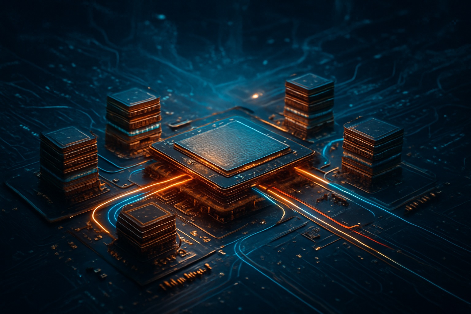
  • Beyond Moore’s Law: How Advanced Packaging is Unlocking the Next Era of AI Performance

    Beyond Moore’s Law: How Advanced Packaging is Unlocking the Next Era of AI Performance

    The relentless march of Artificial Intelligence demands ever-increasing computational power, blazing-fast data transfer, and unparalleled energy efficiency. As traditional silicon scaling, famously known as Moore's Law, approaches its physical and economic limits, the semiconductor industry is turning to a new frontier of innovation: advanced packaging technologies. These groundbreaking techniques are no longer just a back-end process; they are now at the forefront of hardware design, proving crucial for enhancing the performance and efficiency of chips that power the most sophisticated AI and machine learning applications, from large language models to autonomous systems.

    This shift represents an immediate and critical evolution in microelectronics. Without these innovations, the escalating demands of modern AI workloads—which are inherently data-intensive and latency-sensitive—would quickly outstrip the capabilities of conventional chip designs. Advanced packaging solutions are enabling the close integration of processing units and memory, dramatically boosting bandwidth, reducing latency, and overcoming the persistent "memory wall" bottleneck that has historically constrained AI performance. By allowing for higher computational density and more efficient power delivery, these technologies are directly fueling the ongoing AI revolution, making more powerful, energy-efficient, and compact AI hardware a reality.

    Technical Marvels: The Core of AI's Hardware Revolution

    The advancements in chip packaging are fundamentally redefining what's possible in AI hardware. These technologies move beyond the limitations of monolithic 2D designs to achieve unprecedented levels of performance, efficiency, and flexibility.

    2.5D Packaging represents an ingenious intermediate step, where multiple bare dies—such as a Graphics Processing Unit (GPU) and High-Bandwidth Memory (HBM) stacks—are placed side-by-side on a shared silicon or organic interposer. This interposer is a sophisticated substrate etched with fine wiring patterns (Redistribution Layers, or RDLs) and often incorporates Through-Silicon Vias (TSVs) to route signals and power between the dies. Companies like Taiwan Semiconductor Manufacturing Company (TSMC) (NYSE: TSM) with its CoWoS (Chip-on-Wafer-on-Substrate) and Intel (NASDAQ: INTC) with its EMIB (Embedded Multi-die Interconnect Bridge) are pioneers here. This approach drastically shortens signal paths between logic and memory, providing a massive, ultra-wide communication bus critical for data-intensive AI. This directly addresses the "memory wall" problem and significantly improves power efficiency by reducing electrical resistance.

    3D Stacking takes integration a step further, vertically integrating multiple active dies or wafers directly on top of each other. This is achieved through TSVs, which are vertical electrical connections passing through the silicon die, allowing signals to travel directly between stacked layers. The extreme proximity of components via TSVs drastically reduces interconnect lengths, leading to superior system design with improved thermal, electrical, and structural advantages. This translates to maximized integration density, ultra-fast data transfer, and significantly higher bandwidth, all crucial for AI applications that require rapid access to massive datasets.

    Chiplets are small, specialized integrated circuits, each performing a specific function (e.g., CPU, GPU, NPU, specialized memory, I/O). Instead of a single, large monolithic chip, manufacturers assemble these smaller, optimized chiplets into a single multi-chiplet module (MCM) or System-in-Package (SiP) using 2.5D or 3D packaging. High-speed interconnects like Universal Chiplet Interconnect Express (UCIe) enable ultra-fast data exchange. This modular approach allows for unparalleled scalability, flexibility, and optimized performance/power efficiency, as each chiplet can be fabricated with the most suitable process technology. It also improves manufacturing yield and lowers costs by allowing individual components to be tested before integration.

    Hybrid Bonding is a cutting-edge technique that enables direct copper-to-copper and oxide-to-oxide connections between wafers or dies, eliminating traditional solder bumps. This achieves ultra-high interconnect density with pitches below 10 µm, even down to sub-micron levels. This bumpless connection results in vastly expanded I/O and heightened bandwidth (exceeding 1000 GB/s), superior electrical performance, and a reduced form factor. Hybrid bonding is a key enabler for advanced 3D stacking of logic and memory, facilitating unprecedented integration for technologies like TSMC’s SoIC and Intel’s Foveros Direct.

    The AI research community and industry experts have universally hailed these advancements as "critical," "essential," and "transformative." They emphasize that these packaging innovations directly tackle the "memory wall," enable next-generation AI by extending performance scaling beyond transistor miniaturization, and are fundamentally reshaping the industry landscape. While acknowledging challenges like increased design complexity and thermal management, the consensus is that these technologies are indispensable for the future of AI.

    Reshaping the AI Battleground: Impact on Tech Giants and Startups

    Advanced packaging technologies are not just technical marvels; they are strategic assets that are profoundly reshaping the competitive landscape across the AI industry. The ability to effectively integrate and package chips is becoming as vital as the chip design itself, creating new winners and posing significant challenges for those unable to adapt.

    Leading semiconductor players are heavily invested and stand to benefit immensely. TSMC (NYSE: TSM), as the world’s largest contract chipmaker, is a primary beneficiary, investing billions in its CoWoS and SoIC advanced packaging solutions to meet "very strong" demand from HPC and AI clients. Intel (NASDAQ: INTC), through its IDM 2.0 strategy, is pushing its Foveros (3D stacking) and EMIB (2.5D) technologies, offering these services to external customers via Intel Foundry Services. Samsung (KRX: 005930) is aggressively expanding its foundry business, aiming to be a "one-stop shop" for AI chip development, leveraging its SAINT (Samsung Advanced Interconnection Technology) 3D packaging and expertise across memory and advanced logic. AMD (NASDAQ: AMD) extensively uses chiplets in its Ryzen and EPYC processors, and its Instinct MI300A/X series accelerators integrate GPU, CPU, and memory chiplets using 2.5D and 3D packaging for energy-efficient AI. NVIDIA (NASDAQ: NVDA)'s H100 and A100 GPUs, and its newer Blackwell chips, are prime examples leveraging 2.5D CoWoS technology for unparalleled AI performance, demonstrating the critical role of packaging in its market dominance.

    Beyond the chipmakers, tech giants and hyperscalers like Google (NASDAQ: GOOGL), Meta (NASDAQ: META), Amazon (NASDAQ: AMZN), and Tesla (NASDAQ: TSLA) are either developing custom AI chips (e.g., Google's TPUs, Amazon's Trainium and Inferentia) or heavily utilizing third-party accelerators. They directly benefit from the performance and efficiency gains, which are essential for powering their massive data centers and AI services. Amazon, for instance, is increasingly pursuing vertical integration in chip design and manufacturing to gain greater control and optimize for its specific AI workloads, reducing reliance on external suppliers.

    The competitive implications are significant. The battleground is shifting from solely designing the best transistor to effectively integrating and packaging it, making packaging prowess a critical differentiator. Companies with strong foundry ties and early access to advanced packaging capacity gain substantial strategic advantages. This also leads to potential disruption: older technologies relying solely on traditional 2D scaling will struggle to compete, potentially rendering some existing products less competitive. Faster innovation cycles driven by modularity will accelerate hardware turnover. Furthermore, advanced packaging enables entirely new categories of AI products requiring extreme computational density, such as advanced autonomous systems and specialized medical devices. For startups, chiplet technology could lower barriers to entry, allowing them to innovate faster in specialized AI hardware by leveraging pre-designed components rather than designing entire monolithic chips from scratch.

    A New Foundation for AI's Future: Wider Significance

    Advanced packaging is not merely a technical upgrade; it's a foundational shift that underpins the broader AI landscape and its future trends. Its significance extends far beyond individual chip performance, impacting everything from the economic viability of AI deployments to the very types of AI models we can develop.

    At its core, advanced packaging is about extending the trajectory of AI progress beyond the physical limitations of traditional silicon manufacturing. It provides an alternative pathway to continue performance scaling, ensuring that hardware infrastructure can keep pace with the escalating computational demands of complex AI models. This is particularly crucial for the development and deployment of ever-larger large language models and increasingly sophisticated generative AI applications. By enabling heterogeneous integration and specialized chiplets, it fosters a new era of purpose-built AI hardware, where processors are precisely optimized for specific tasks, leading to unprecedented efficiency and performance gains. This contrasts sharply with the general-purpose computing paradigm that often characterized earlier AI development.

    The impact on AI's capabilities is profound. The ability to dramatically increase memory bandwidth and reduce latency, facilitated by 2.5D and 3D stacking with HBM, directly translates to faster AI training times and more responsive inference. This not only accelerates research and development but also makes real-time AI applications more feasible and widespread. For instance, advanced packaging is essential for enabling complex multi-agent AI workflow orchestration, as offered by TokenRing AI, which requires seamless, high-speed communication between various processing units.

    However, this transformative shift is not without its potential concerns. The cost of initial mass production for advanced packaging can be high due to complex processes and significant capital investment. The complexity of designing, manufacturing, and testing multi-chiplet, 3D-stacked systems introduces new engineering challenges, including managing increased variation, achieving precision in bonding, and ensuring effective thermal management for densely packed components. The supply chain also faces new vulnerabilities, requiring unprecedented collaboration and standardization across multiple designers, foundries, and material suppliers. Recent "capacity crunches" in advanced packaging, particularly for high-end AI chips, underscore these challenges, though major industry investments aim to stabilize supply into late 2025 and 2026.

    Comparing its importance to previous AI milestones, advanced packaging stands as a hardware-centric breakthrough akin to the advent of GPUs (e.g., NVIDIA's CUDA in 2006) for deep learning. While GPUs provided the parallel processing power that unlocked the deep learning revolution, advanced packaging provides the essential physical infrastructure to realize and deploy today's and tomorrow's sophisticated AI models at scale, pushing past the fundamental limits of traditional silicon. It's not merely an incremental improvement but a new paradigm shift, moving from monolithic scaling to modular optimization, securing the hardware foundation for AI's continued exponential growth.

    The Horizon: Future Developments and Predictions

    The trajectory of advanced packaging technologies promises an even more integrated, modular, and specialized future for AI hardware. The innovations currently in research and development will continue to push the boundaries of what AI systems can achieve.

    In the near-term (1-5 years), we can expect broader adoption of chiplet-based designs, supported by the maturation of standards like the Universal Chiplet Interconnect Express (UCIe), fostering a more robust and interoperable ecosystem. Heterogeneous integration, particularly 2.5D and 3D hybrid bonding, will become standard for high-performance AI and HPC systems, with hybrid bonding proving vital for next-generation High-Bandwidth Memory (HBM4), anticipated for full commercialization in late 2025. Innovations in novel substrates, such as glass-core technology and fan-out panel-level packaging (FOPLP), will also continue to shape the industry.

    Looking further into the long-term (beyond 5 years), the semiconductor industry is poised for a transition to fully modular designs dominated by custom chiplets, specifically optimized for diverse AI workloads. Widespread 3D heterogeneous computing, including the vertical stacking of GPU tiers, DRAM, and other integrated components using TSVs, will become commonplace. We will also see the integration of emerging technologies like quantum computing and photonics, including co-packaged optics (CPO) for ultra-high bandwidth communication, pushing technological boundaries. Intriguingly, AI itself will play an increasingly critical role in optimizing chiplet-based semiconductor design, leveraging machine learning for power, performance, and thermal efficiency layouts.

    These developments will unlock a plethora of potential applications and use cases. High-Performance Computing (HPC) and data centers will achieve unparalleled speed and energy efficiency, crucial for the escalating demands of generative AI and LLMs. Modularity and power efficiency will significantly benefit edge AI devices, enabling real-time processing in autonomous systems, industrial IoT, and portable devices. Specialized AI accelerators will become even more powerful and energy-efficient, driving advancements across transformative industries like healthcare, quantum computing, and neuromorphic computing.

    Despite this promising outlook, remaining challenges need addressing. Thermal management remains a critical hurdle due to increased power density in 3D ICs, necessitating innovative cooling solutions like advanced thermal interface materials, lidless chip designs, and liquid cooling. Standardization across the chiplet ecosystem is crucial, as the lack of universal standards for interconnects and the complex coordination required for integrating multiple dies from different vendors pose significant barriers. While UCIe is a step forward, greater industry collaboration is essential. The cost of initial mass production for advanced packaging can also be high, and manufacturing complexities, including ensuring high yields and a shortage of specialized packaging engineers, are ongoing concerns.

    Experts predict that advanced packaging will be a critical front-end innovation driver, fundamentally powering the AI revolution and extending performance scaling. The package itself is becoming a crucial point of innovation and a differentiator for system performance. The market for advanced packaging, especially high-end 2.5D/3D approaches, is projected for significant growth, estimated to reach approximately $75 billion by 2033 from about $15 billion in 2025, with AI applications accounting for a substantial and growing portion. Chiplet-based designs are expected to be found in almost all high-performance computing systems and will become the new standard for complex AI systems.

    The Unsung Hero: A Comprehensive Wrap-Up

    Advanced packaging technologies have emerged as the unsung hero of the AI revolution, providing the essential hardware infrastructure that allows algorithmic and software breakthroughs to flourish. This fundamental shift in microelectronics is not merely an incremental improvement; it is a pivotal moment in AI history, redefining how computational power is delivered and ensuring that the relentless march of AI innovation can continue beyond the limits of traditional silicon scaling.

    The key takeaways are clear: advanced packaging is indispensable for sustaining AI innovation, effectively overcoming the "memory wall" by boosting memory bandwidth, enabling the creation of highly specialized and energy-efficient AI hardware, and representing a foundational shift from monolithic chip design to modular optimization. These technologies, including 2.5D/3D stacking, chiplets, and hybrid bonding, are collectively driving unparalleled performance enhancements, significantly lower power consumption, and reduced latency—all critical for the demanding workloads of modern AI.

    Assessing its significance in AI history, advanced packaging stands as a hardware milestone comparable to the advent of GPUs for deep learning. Just as GPUs provided the parallel processing power needed for deep neural networks, advanced packaging provides the necessary physical infrastructure to realize and deploy today's and tomorrow's sophisticated AI models at scale. Without these innovations, the escalating computational, memory bandwidth, and ultra-low latency demands of complex AI models like LLMs would be increasingly difficult to meet. It is the critical enabler that has allowed hardware innovation to keep pace with the exponential growth of AI software and applications.

    The long-term impact will be transformative. We can anticipate the dominance of chiplet-based designs, fostering a robust and interoperable ecosystem that could lower barriers to entry for AI startups. This will lead to sustained acceleration in AI capabilities, enabling more powerful AI models and broader application across various industries. The widespread integration of co-packaged optics will become commonplace, addressing ever-growing bandwidth requirements, and AI itself will play a crucial role in optimizing chiplet-based semiconductor design. The industry is moving towards full 3D heterogeneous computing, integrating emerging technologies like quantum computing and advanced photonics, further pushing the boundaries of AI hardware.

    In the coming weeks and months, watch for the accelerated adoption of 2.5D and 3D hybrid bonding as standard practice for high-performance AI. Monitor the maturation of the chiplet ecosystem and interconnect standards like UCIe, which will be vital for interoperability. Keep an eye on the impact of significant investments by industry giants like TSMC, Intel, and Samsung, which are aimed at easing the current advanced packaging capacity crunch and improving supply chain stability into late 2025 and 2026. Furthermore, innovations in thermal management solutions and novel substrates like glass-core technology will be crucial areas of development. Finally, observe the progress in co-packaged optics (CPO), which will be essential for addressing the ever-growing bandwidth requirements of future AI systems.

    These developments underscore advanced packaging's central role in the AI revolution, positioning it as a key battlefront in semiconductor innovation that will continue to redefine the capabilities of AI hardware and, by extension, the future of artificial intelligence itself.

    This content is intended for informational purposes only and represents analysis of current AI developments.

    TokenRing AI delivers enterprise-grade solutions for multi-agent AI workflow orchestration, AI-powered development tools, and seamless remote collaboration platforms. For more information, visit https://www.tokenring.ai/.

  • Advanced Packaging: Unlocking the Next Era of Chip Performance for AI

    Advanced Packaging: Unlocking the Next Era of Chip Performance for AI

    The artificial intelligence landscape is undergoing a profound transformation, driven not just by algorithmic breakthroughs but by a quiet revolution in semiconductor manufacturing: advanced packaging. Innovations such as 3D stacking and heterogeneous integration are fundamentally reshaping how AI chips are designed and built, delivering unprecedented gains in performance, power efficiency, and form factor. These advancements are critical for overcoming the physical limitations of traditional silicon scaling, often referred to as "Moore's Law limits," and are enabling the development of the next generation of AI models, from colossal large language models (LLMs) to sophisticated generative AI.

    This shift is immediately significant because modern AI workloads demand insatiable computational power, vast memory bandwidth, and ultra-low latency, requirements that conventional 2D chip designs are increasingly struggling to meet. By allowing for the vertical integration of components and the modular assembly of specialized chiplets, advanced packaging is breaking through these bottlenecks, ensuring that hardware innovation continues to keep pace with the rapid evolution of AI software and applications.

    The Engineering Marvels: 3D Stacking and Heterogeneous Integration

    At the heart of this revolution are two interconnected yet distinct advanced packaging techniques: 3D stacking and heterogeneous integration. These methods represent a significant departure from the traditional 2D monolithic chip designs, where all components are laid out side-by-side on a single silicon die.

    3D Stacking, also known as 3D Integrated Circuits (3D ICs) or 3D packaging, involves vertically stacking multiple semiconductor dies or wafers on top of each other. The magic lies in Through-Silicon Vias (TSVs), which are vertical electrical connections passing directly through the silicon dies, allowing for direct communication and power transfer between layers. These TSVs drastically shorten interconnect distances, leading to faster data transfer speeds, reduced signal propagation delays, and significantly lower latency. For instance, TSVs can have diameters around 10µm and depths of 50µm, with pitches around 50µm. Cutting-edge techniques like hybrid bonding, which enables direct copper-to-copper (Cu-Cu) connections at the wafer level, push interconnect pitches into the single-digit micrometer range, supporting bandwidths up to 1000 GB/s. This vertical integration is crucial for High-Bandwidth Memory (HBM), where multiple DRAM dies are stacked and connected to a logic base die, providing unparalleled memory bandwidth to AI processors.

    Heterogeneous Integration, on the other hand, is the process of combining diverse semiconductor technologies, often from different manufacturers and even different process nodes, into a single, closely interconnected package. This is primarily achieved through the use of "chiplets" – smaller, specialized chips each performing a specific function (e.g., CPU, GPU, NPU, specialized memory, I/O). These chiplets are then assembled into a multi-chiplet module (MCM) or System-in-Package (SiP) using advanced packaging technologies such as 2.5D packaging. In 2.5D packaging, multiple bare dies (like a GPU and HBM stacks) are placed side-by-side on a common interposer (silicon, organic, or glass) that routes signals between them. This modular approach allows for the optimal technology to be selected for each function, balancing performance, power, and cost. For example, a high-performance logic chiplet might use a cutting-edge 3nm process, while an I/O chiplet could use a more mature, cost-effective 28nm node.

    The difference from traditional 2D monolithic designs is stark. While 2D designs rely on shrinking transistors (CMOS scaling) on a single plane, advanced packaging extends scaling by increasing functional density vertically and enabling modularity. This not only improves yield (smaller chiplets mean fewer defects impact the whole system) but also allows for greater flexibility and customization. Initial reactions from the AI research community and industry experts have been overwhelmingly positive, recognizing these advancements as "critical" and "essential for sustaining the rapid pace of AI development." They emphasize that 3D stacking and heterogeneous integration directly address the "memory wall" problem and are key to enabling specialized, energy-efficient AI hardware.

    Reshaping the AI Industry: Competitive Implications and Strategic Advantages

    The advent of advanced packaging is profoundly reshaping the competitive landscape for AI companies, tech giants, and startups alike. It is no longer just about who can design the best chip, but who can effectively integrate and package it.

    Leading foundries and advanced packaging providers like Taiwan Semiconductor Manufacturing Company (TSMC) (NYSE: TSM), Intel Corporation (NASDAQ: INTC), and Samsung Electronics Co., Ltd. (KRX: 005930) are at the forefront, making massive investments. TSMC, with its dominant CoWoS (Chip-on-Wafer-on-Substrate) and SoIC (System on Integrated Chips) technologies, is expanding capacity rapidly, aiming to become a "System Fab" offering comprehensive AI chip manufacturing. Intel, through its IDM 2.0 strategy and advanced packaging solutions like Foveros (3D stacking) and EMIB (Embedded Multi-die Interconnect Bridge, a 2.5D solution), is aggressively pursuing leadership and offering these services to external customers via Intel Foundry Services (IFS). Samsung is also restructuring its chip packaging processes for a "one-stop shop" approach, integrating memory, foundry, and advanced packaging to reduce production time and offer differentiated capabilities, as seen in its strategic partnership with OpenAI.

    AI hardware developers such as NVIDIA Corporation (NASDAQ: NVDA) and Advanced Micro Devices, Inc. (NASDAQ: AMD) are primary beneficiaries and drivers of this demand. NVIDIA's H100 and A100 series GPUs, and its newer Blackwell chips, are prime examples leveraging 2.5D CoWoS technology for unparalleled AI performance. AMD extensively employs chiplets in its Ryzen and EPYC processors, and its Instinct MI300A/X series accelerators integrate GPU, CPU, and memory chiplets using advanced 2.5D and 3D packaging techniques, including hybrid bonding for 3D V-Cache. Tech giants and hyperscalers like Alphabet Inc. (NASDAQ: GOOGL) (Google), Amazon.com, Inc. (NASDAQ: AMZN), and Microsoft Corporation (NASDAQ: MSFT) are leveraging advanced packaging for their custom AI chips (e.g., Google's Tensor Processing Units or TPUs, Microsoft's Azure Maia 100), gaining significant strategic advantages through vertical integration.

    This shift is creating a new competitive battleground where packaging prowess is a key differentiator. Companies with strong ties to leading foundries and early access to advanced packaging capacities hold a significant strategic advantage. The industry is moving from monolithic to modular designs, fundamentally altering the semiconductor value chain and redefining performance limits. This also means existing products relying solely on older 2D scaling methods will struggle to compete. For AI startups, chiplet technology lowers the barrier to entry, enabling faster innovation in specialized AI hardware by leveraging pre-designed components.

    Wider Significance: Powering the AI Revolution

    Advanced packaging innovations are not just incremental improvements; they represent a foundational shift that underpins the entire AI landscape. Their wider significance lies in their ability to address fundamental physical limitations, thereby enabling the continued rapid evolution and deployment of AI.

    Firstly, these technologies are crucial for extending Moore's Law, which has historically driven exponential growth in computing power by shrinking transistors. As transistor scaling faces increasing physical and economic limits, advanced packaging provides an alternative pathway for performance gains by increasing functional density vertically and enabling modular optimization. This ensures that the hardware infrastructure can keep pace with the escalating computational demands of increasingly complex AI models like LLMs and generative AI.

    Secondly, the ability to overcome the "memory wall" through 2.5D and 3D stacking with HBM is paramount. AI workloads are inherently memory-intensive, and the speed at which data can be moved between processors and memory often bottlenecks performance. Advanced packaging dramatically boosts memory bandwidth and reduces latency, directly translating to faster AI training and inference.

    Thirdly, heterogeneous integration fosters specialized and energy-efficient AI hardware. By allowing the combination of diverse, purpose-built processing units, manufacturers can create highly optimized chips tailored for specific AI tasks. This flexibility enables the development of energy-efficient solutions, which is critical given the massive power consumption of modern AI data centers. Chiplet-based designs can offer 30-40% lower energy consumption for the same workload compared to monolithic designs.

    However, this paradigm shift also brings potential concerns. The increased complexity of designing and manufacturing multi-chiplet, 3D-stacked systems introduces challenges in supply chain coordination, yield management, and thermal dissipation. Integrating multiple dies from different vendors requires unprecedented collaboration and standardization. While long-term costs may be reduced, initial mass-production costs for advanced packaging can be high. Furthermore, thermal management becomes a significant hurdle, as increased component density generates more heat, requiring innovative cooling solutions.

    Comparing its importance to previous AI milestones, advanced packaging stands as a hardware-centric breakthrough that complements and enables algorithmic advancements. Just as the development of GPUs (like NVIDIA's CUDA in 2006) provided the parallel processing power necessary for the deep learning revolution, advanced packaging provides the necessary physical infrastructure to realize and deploy today's sophisticated AI models at scale. It's the "unsung hero" powering the next-generation AI revolution, allowing AI to move from theoretical breakthroughs to widespread practical applications across industries.

    The Horizon: Future Developments and Uncharted Territory

    The trajectory of advanced packaging innovations points towards a future of even greater integration, modularity, and specialization, profoundly impacting the future of AI.

    In the near-term (1-5 years), we can expect broader adoption of chiplet-based designs across a wider range of processors, driven by the maturation of standards like Universal Chiplet Interconnect Express (UCIe), which will foster a more robust and interoperable chiplet ecosystem. Sophisticated heterogeneous integration, particularly 2.5D and 3D hybrid bonding, will become standard for high-performance AI and HPC systems. Hybrid bonding, with its ultra-dense, sub-10-micrometer interconnect pitches, is critical for next-generation HBM and 3D ICs. We will also see continued evolution in interposer technology, with active interposers (containing transistors) gradually replacing passive ones.

    Long-term (beyond 5 years), the industry is poised for fully modular semiconductor designs, dominated by custom chiplets optimized for specific AI workloads. A full transition to widespread 3D heterogeneous computing, including vertical stacking of GPU tiers, DRAM, and integrated components using TSVs, will become commonplace. The integration of emerging technologies like quantum computing and photonics, including co-packaged optics (CPO) for ultra-high bandwidth communication, will further push the boundaries. AI itself will play an increasingly crucial role in optimizing chiplet-based semiconductor design, leveraging machine learning for power, performance, and thermal efficiency layouts.

    These advancements will unlock new potential applications and use cases for AI. High-Performance Computing (HPC) and data centers will see unparalleled speed and energy efficiency, crucial for the ever-growing demands of generative AI and LLMs. Edge AI devices will benefit from the modularity and power efficiency, enabling real-time processing in autonomous systems, industrial IoT, and portable devices. Specialized AI accelerators will become even more powerful and energy-efficient, while healthcare, quantum computing, and neuromorphic computing will leverage these chips for transformative applications.

    However, significant challenges still need to be addressed. Thermal management remains a critical hurdle, as increased power density in 3D ICs creates hotspots, necessitating innovative cooling solutions and integrated thermal design workflows. Power delivery to multiple stacked dies is also complex. Manufacturing complexities, ensuring high yields in bonding processes, and the need for advanced Electronic Design Automation (EDA) tools capable of handling multi-dimensional optimization are ongoing concerns. The lack of universal standards for interconnects and a shortage of specialized packaging engineers also pose barriers.

    Experts are overwhelmingly positive, predicting that advanced packaging will be a critical front-end innovation driver, fundamentally powering the AI revolution and extending performance scaling beyond traditional transistor miniaturization. The package itself will become a crucial point of innovation and a differentiator for system performance. The market for advanced packaging, especially high-end 2.5D/3D approaches, is projected for significant growth, reaching approximately $75 billion by 2033 from an estimated $15 billion in 2025.

    A New Era of AI Hardware: The Path Forward

    The revolution in advanced semiconductor packaging, encompassing 3D stacking and heterogeneous integration, marks a pivotal moment in the history of Artificial Intelligence. It is the essential hardware enabler that ensures the relentless march of AI innovation can continue, pushing past the physical constraints that once seemed insurmountable.

    The key takeaways are clear: advanced packaging is critical for sustaining AI innovation beyond Moore's Law, overcoming the "memory wall," enabling specialized and efficient AI hardware, and driving unprecedented gains in performance, power, and cost efficiency. This isn't just an incremental improvement; it's a foundational shift that redefines how computational power is delivered, moving from monolithic scaling to modular optimization.

    The long-term impact will see chiplet-based designs become the new standard for complex AI systems, leading to sustained acceleration in AI capabilities, widespread integration of co-packaged optics, and an increasing reliance on AI-driven design automation. This will unlock more powerful AI models, broader application across industries, and the realization of truly intelligent systems.

    In the coming weeks and months, watch for accelerated adoption of 2.5D and 3D hybrid bonding as standard practice, particularly for high-performance AI and HPC. Keep an eye on the maturation of the chiplet ecosystem and interconnect standards like UCIe, which will foster greater interoperability and flexibility. Significant investments from industry giants like TSMC, Intel, and Samsung are aimed at easing the advanced packaging capacity crunch, which is expected to gradually improve supply chain stability for AI hardware manufacturers into late 2025 and 2026. Furthermore, innovations in thermal management, panel-level packaging, and novel substrates like glass-core technology will continue to shape the future. The convergence of these innovations promises a new era of AI hardware, one that is more powerful, efficient, and adaptable than ever before.


    This content is intended for informational purposes only and represents analysis of current AI developments.

    TokenRing AI delivers enterprise-grade solutions for multi-agent AI workflow orchestration, AI-powered development tools, and seamless remote collaboration platforms. For more information, visit https://www.tokenring.ai/.