Tag: 5G

  • India’s Tech Renaissance: Academic-Industry Partnerships Propel Nation to Global Innovation Forefront

    India’s Tech Renaissance: Academic-Industry Partnerships Propel Nation to Global Innovation Forefront

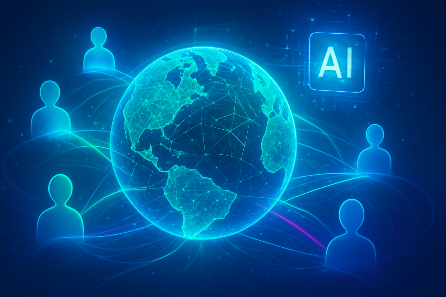
    India is rapidly asserting its position as a global powerhouse in technological innovation, transcending its traditional role as an IT services hub to become a formidable force in cutting-edge research and development. This transformation is fueled by a dynamic ecosystem of academic institutions, government bodies, and industry players forging strategic collaborations that are pushing the boundaries of what's possible. At the forefront of this burgeoning landscape is the Indian Institute of Information Technology, Allahabad (IIIT-A), a beacon of regional tech innovation whose multifaceted partnerships are yielding significant advancements across critical sectors.

    The immediate significance of these developments lies in their dual impact: fostering a new generation of skilled talent and translating theoretical research into practical, impactful solutions. From pioneering digital public infrastructure to making strides in artificial intelligence, space technology, and advanced communication systems, India's concerted efforts are not only addressing domestic challenges but also setting new benchmarks on the global stage. The collaborative model championed by institutions like IIIT-A is proving instrumental in accelerating this progress, bridging the gap between academia and industry to create an environment ripe for disruptive innovation.

    Deep Dive into India's R&D Prowess: The IIIT-A Blueprint

    India's technological leap is characterized by focused research and development initiatives across a spectrum of high-impact areas. Beyond the widely recognized success of its Digital Public Infrastructure (DPI) like the Unified Payments Interface (UPI) and Aadhaar, the nation is making substantial inroads in Artificial Intelligence (AI) and Machine Learning (ML), Space Technology, 5G/6G communications, Healthcare Technology, and Cybersecurity. Institutions like IIIT-A are pivotal in this evolution, engaging in diverse collaborations that underscore a commitment to both foundational research and applied innovation.

    IIIT-A's technical contributions are particularly noteworthy in AI and Deep Learning, Robotics, and Cybersecurity. For instance, its partnership with the Naval Science and Technological Laboratory (NSTL), Vishakhapatnam (a Defence Research and Development Organisation (DRDO) lab), is developing advanced Deep Learning and AI solutions for identifying marine life, objects, and underwater structures—a critical advancement for defense and marine research. This initiative, supported by the Naval Research Board (NRB), showcases a direct application of AI to strategic national security interests. Furthermore, IIIT-A has established an AI-STEM Innovation Center in collaboration with STEMLearn.AI (Teevra EduTech Pvt. Ltd.), focusing on joint R&D, curriculum design, and capacity building in robotics, AI, ML, and data science. This approach differs significantly from previous models by embedding industry needs directly into academic research and training, ensuring that graduates are "industry-ready" and research is directly applicable. Initial reactions from the AI research community highlight the strategic importance of such partnerships in accelerating practical AI deployment and fostering a robust talent pipeline, particularly in specialized domains like defense and industrial automation.

    The institute's Center for Intelligent Robotics, established in 2001, has consistently worked on world-class research and product development, with a special emphasis on Healthcare Automation, equipped with advanced infrastructure including humanoid robots. In cybersecurity, the Network Security & Cryptography (NSC) Lab at IIIT-A focuses on developing techniques and algorithms to protect network infrastructure, with research areas spanning cryptanalysis, blockchain, and novel security solutions, including IoT Security. These initiatives demonstrate a holistic approach to technological advancement, combining theoretical rigor with practical application, distinguishing India's current R&D thrust from earlier, more fragmented efforts. The emphasis on indigenous development, particularly in strategic sectors like defense and space, also marks a significant departure, aiming for greater self-reliance and global competitiveness.

    Competitive Landscape: Shifting Tides for Tech Giants and Startups

    The proliferation of advanced technological research and development originating from India, exemplified by institutions like IIIT-A, is poised to significantly impact both established AI companies and a new wave of startups. Indian tech giants, particularly those with a strong R&D focus, stand to benefit immensely from the pool of highly skilled talent emerging from these academic-industry collaborations. Companies like Tata Consultancy Services (TCS) (NSE: TCS, BSE: 532540), already collaborating with IIIT-A on Machine Learning electives, will find a ready workforce capable of driving their next-generation AI and software development projects. Similarly, Infosys (NSE: INFY, BSE: 500209), which has endowed the Infosys Center for Artificial Intelligence at IIIT-Delhi, is strategically investing in the very source of future AI innovation.

    The competitive implications for major AI labs and global tech companies are multifaceted. While many have established their own research centers in India, the rise of indigenous R&D, particularly in areas like ethical AI, local language processing (e.g., BHASHINI), and domain-specific applications (like AgriTech and rural healthcare), could foster a unique competitive advantage for Indian firms. This focus on "AI for India" can lead to solutions that are more tailored to local contexts and scalable across emerging markets, potentially disrupting existing products or services offered by global players that may not fully address these specific needs. Startups emerging from this ecosystem, often with faculty involvement, are uniquely positioned to leverage cutting-edge research to solve real-world problems, creating niche markets and offering specialized solutions that could challenge established incumbents.

    Furthermore, the emphasis on Digital Public Infrastructure (DPI) and open-source contributions, such as those related to UPI, positions India as a leader in creating scalable, inclusive digital ecosystems. This could influence global standards and provide a blueprint for other developing nations, giving Indian companies a strategic advantage in exporting their expertise and technology. The involvement of defense organizations like DRDO and ISRO in collaborations with IIIT-A also points to a strengthening of national capabilities in strategic technologies, potentially reducing reliance on foreign imports and fostering a robust domestic defense-tech industry. This market positioning highlights India's ambition not just to consume technology but to innovate and lead in its creation.

    Broader Significance: Shaping the Global AI Narrative

    The technological innovations stemming from India, particularly those driven by academic-industry collaborations like IIIT-A's, are deeply embedded within and significantly shaping the broader global AI landscape. India's unique approach, often characterized by a focus on "AI for social good" and scalable, inclusive solutions, positions it as a critical voice in the ongoing discourse about AI's ethical development and deployment. The nation's leadership in digital public goods, exemplified by UPI and Aadhaar, serves as a powerful model for how technology can be leveraged for widespread public benefit, influencing global trends towards digital inclusion and accessible services.

    The impacts of these developments are far-reaching. On one hand, they promise to uplift vast segments of India's population through AI-powered healthcare, AgriTech, and language translation tools, addressing critical societal challenges with innovative, cost-effective solutions. On the other hand, potential concerns around data privacy, algorithmic bias, and the equitable distribution of AI's benefits remain pertinent, necessitating robust ethical frameworks—an area where India is actively contributing to global discussions, planning to host a Global AI Summit in February 2026. This proactive stance on ethical AI is crucial in preventing the pitfalls observed in earlier technological revolutions.

    Comparing this to previous AI milestones, India's current trajectory marks a shift from being primarily a consumer or implementer of AI to a significant contributor to its foundational research and application. While past breakthroughs often originated from a few dominant tech hubs, India's distributed innovation model, leveraging institutions across the country, democratizes AI development. This decentralized approach, combined with a focus on indigenous solutions and open standards, could lead to a more diverse and resilient global AI ecosystem, less susceptible to monopolistic control. The development of platforms like BHASHINI for language translation directly addresses a critical gap for multilingual societies, setting a precedent for inclusive AI development that goes beyond dominant global languages.

    The Road Ahead: Anticipating Future Breakthroughs and Challenges

    Looking ahead, the trajectory of technological innovation in India, particularly from hubs like IIIT-A, promises exciting near-term and long-term developments. In the immediate future, we can expect to see further maturation and deployment of AI solutions in critical sectors. The ongoing collaborations in AI for rural healthcare, for instance, are likely to lead to more sophisticated diagnostic tools, personalized treatment plans, and widespread adoption of telemedicine platforms, significantly improving access to quality healthcare in underserved areas. Similarly, advancements in AgriTech, driven by AI and satellite imagery, will offer more precise crop management, weather forecasting, and market insights, bolstering food security and farmer livelihoods.

    On the horizon, potential applications and use cases are vast. The research in advanced communication systems, particularly 6G technology, supported by initiatives like the Bharat 6G Mission, suggests India will play a leading role in defining the next generation of global connectivity, enabling ultra-low latency applications for autonomous vehicles, smart cities, and immersive digital experiences. Furthermore, IIIT-A's work in robotics, especially in healthcare automation, points towards a future with more intelligent assistive devices and automated surgical systems. The deep collaboration with defense organizations also indicates a continuous push for indigenous capabilities in areas like drone technology, cyber warfare, and advanced surveillance systems, enhancing national security.

    However, challenges remain. Scaling these innovations across a diverse and geographically vast nation requires significant investment in infrastructure, digital literacy, and equitable access to technology. Addressing ethical considerations, ensuring data privacy, and mitigating algorithmic bias will be ongoing tasks, requiring continuous policy development and public engagement. Experts predict that India's "innovation by necessity" approach, focused on solving unique domestic challenges with cost-effective solutions, will increasingly position it as a global leader in inclusive and sustainable technology. The next phase will likely involve deeper integration of AI across all sectors, the emergence of more specialized AI startups, and India's growing influence in shaping global technology standards and governance frameworks.

    Conclusion: India's Enduring Impact on the AI Frontier

    India's current wave of technological innovation, spearheaded by institutions like the Indian Institute of Information Technology, Allahabad (IIIT-A) and its strategic collaborations, marks a pivotal moment in the nation's journey towards becoming a global technology leader. The key takeaways from this transformation are clear: a robust emphasis on indigenous research and development, a concerted effort to bridge the academia-industry gap, and a commitment to leveraging advanced technologies like AI for both national security and societal good. The success of Digital Public Infrastructure and the burgeoning ecosystem of AI-driven solutions underscore India's capability to innovate at scale and with significant impact.

    This development holds profound significance in the annals of AI history. It demonstrates a powerful model for how emerging economies can not only adopt but also actively shape the future of artificial intelligence, offering a counter-narrative to the traditionally concentrated hubs of innovation. India's focus on ethical AI and inclusive technology development provides a crucial blueprint for ensuring that the benefits of AI are widely shared and responsibly managed globally. The collaborative spirit, particularly evident in IIIT-A's partnerships with government, industry, and international academia, is a testament to the power of collective effort in driving technological progress.

    In the coming weeks and months, the world should watch for continued advancements from India in AI-powered public services, further breakthroughs in defense and space technologies, and the increasing global adoption of India's digital public goods model. The nation's strategic investments in 6G and emerging technologies signal an ambitious vision to remain at the forefront of the technological revolution. India is not just participating in the global tech race; it is actively defining new lanes and setting new paces, promising a future where innovation is more distributed, inclusive, and impactful for humanity.


    This content is intended for informational purposes only and represents analysis of current AI developments.

    TokenRing AI delivers enterprise-grade solutions for multi-agent AI workflow orchestration, AI-powered development tools, and seamless remote collaboration platforms.
    For more information, visit https://www.tokenring.ai/.

  • Jio’s Global 5G Revolution: Low-Cost Connectivity Meets AI for All

    Jio’s Global 5G Revolution: Low-Cost Connectivity Meets AI for All

    Reliance Jio Platforms, a subsidiary of Reliance Industries Limited (NSE: RELIANCE, BSE: 500325), is spearheading a transformative global expansion with its indigenously developed, low-cost 5G technology, profoundly impacting telecommunications accessibility and infrastructure worldwide. This aggressive strategy, built on a foundation of disruptive pricing and widespread digital adoption in India, is now poised to democratize advanced connectivity and artificial intelligence on a global scale, particularly in underserved regions.

    The company's approach involves exporting its battle-tested, homegrown 5G technology stack, promising significant cost reductions for global operators and challenging the long-standing dominance of traditional telecom equipment vendors. Coupled with an ambitious "AI Everywhere for Everyone" vision, Jio is not merely deploying 5G but integrating cutting-edge AI capabilities, from network optimization to consumer-facing generative AI, creating a powerful synergy that could redefine the future of digital services.

    Technical Prowess: Jio's Homegrown 5G and AI-Native Architecture

    Jio's 5G advancement is distinguished by its Standalone (SA) 5G architecture, a "True-5G" approach that operates independently of its 4G infrastructure, offering superior capabilities like ultra-low latency and massive machine-to-machine communication. This is a significant departure from many initial global 5G deployments that adopted Non-Standalone (NSA) architecture, which relies on existing 4G core networks. Jio's network promises speeds up to 10 Gbps and latency under 1 millisecond, leveraging a multi-band spectrum strategy across low-band (700 MHz), mid-band (3.5 GHz), and mmWave (26 GHz) frequencies for optimal coverage and capacity.

    A hallmark of Jio's strategy is its homegrown, end-to-end 5G technology stack, developed "from scratch." This comprehensive suite includes 5G radio, core network solutions, Operational Support Systems (OSS), Business Support Systems (BSS), small cells, and cloud platforms. This indigenous development significantly reduces reliance on multinational vendors like Ericsson (NASDAQ: ERIC) and Nokia (NYSE: NOK), mitigating vendor lock-in and slashing costs by avoiding import duties and IP royalties. The stack is designed to be cloud-native, software-defined, replicable, and modular, making it highly attractive for global operators seeking economical 5G deployment. The company's Fixed Wireless Access (FWA) service, JioAirFiber, further exemplifies this, delivering gigabit-speed broadband wirelessly and serving over 1 million homes per month without extensive fiber optic cabling.

    AI-powered optimization is deeply embedded in Jio's 5G network. The "JioBrain" platform, an advanced AI system, seamlessly integrates with 5G networks to drive operational excellence. It utilizes AI/ML for network planning, resource optimization, predictive maintenance, and real-time decision-making. JioBrain also enhances customer experience through intelligent insights, personalized service recommendations, and robust fraud detection. The company employs a 5G Network Data Analytics Function (NWDAF) and a RAN Intelligent Controller (RIC) with AI/ML algorithms to customize radio access network functionality. This extensive use of AI, including generative AI across various operations, positions Jio at the forefront of intelligent network management. Initial reactions from industry experts, including a Jefferies report on November 7, 2025, commend Jio's cost-effective, homegrown solutions as a "global sensation" with substantial export potential, particularly in developing markets.

    Competitive Ripples: Reshaping the Telecom and Tech Landscape

    Jio's global low-cost 5G expansion is set to send significant competitive ripples across the telecommunications and technology industries. Its disruptive pricing model, previously witnessed in the Indian 4G market, is expected to intensify competition for incumbent telecom operators worldwide. Jio's integrated digital ecosystem, including offerings like Jio Smart Home and JioTV+, combined with its aggressive FWA deployment, could disrupt traditional home broadband and digital service markets. The company's strategic advantages lie in its end-to-end homegrown 5G stack, promising 50-60% cost savings, and its proven ability to rapidly deploy 5G at scale.

    For tech giants, the impact is bifurcated. Companies like Qualcomm (NASDAQ: QCOM) stand to benefit from partnerships with Jio in developing affordable 5G devices. Strategic investors like Alphabet (NASDAQ: GOOGL), through Google, and Meta Platforms (NASDAQ: META) in Jio Platforms, indicate opportunities in cloud services, AI development, and digital ecosystems. Google's partnership to offer Gemini AI assistant free for 18 months to Jio 5G subscribers, announced around October/November 2025, represents the largest AI rollout in a single market. However, traditional telecom vendors such as Ericsson (NASDAQ: ERIC) and Nokia (NYSE: NOK), and Huawei face significant competitive pressure. Jio's move to domestically manufacture its own 5G network products directly reduces its dependence on these global players and positions its in-house solutions as a direct competitor in the global market, potentially shifting market share, especially in markets embracing open architectures.

    Startups will find both opportunities and challenges. Jio's commitment to "AI Everywhere for Everyone" and its plans to digitize Indian businesses with scalable platforms will likely open new avenues for startups focusing on AI, IoT, smart cities, and other digital services. However, they may also face intense competition if Jio expands its direct service offerings into their niches. A Jefferies report on November 7, 2025, highlighted Jio Platforms' potential for robust growth, forecasting an 18-21% CAGR in revenues and EBITDA for FY26-28, driven by tariff increases, FWA growth, and the monetization of its tech stack, signaling a strong market position ahead of its anticipated IPO in H1 2026.

    Broader Horizons: Connectivity, AI, and Global Implications

    Jio's strategy of low-cost 5G expansion coupled with deep AI integration carries profound significance for global connectivity and the broader AI landscape. By offering an affordable and scalable 5G technology stack, Jio can significantly accelerate 5G adoption in developing nations, bridging the digital divide and fostering economic growth where traditional deployments have been cost-prohibitive. Its emphasis on Fixed Wireless Access (FWA) further expands broadband penetration, particularly in regions lacking extensive fiber infrastructure. Jio is also actively contributing to 3GPP standards for 5G and 6G, aiming to shape future global connectivity standards.

    The AI-powered aspects, particularly the "JioBrain" platform and the "AI Everywhere for Everyone" vision, position Jio at the forefront of integrating AI into core infrastructure and services. By offering AI as a service at low costs, Jio aims to dramatically lower the barrier to entry for AI adoption, mirroring its success in democratizing internet access. The partnership with Google to provide free access to Gemini AI Pro to eligible Jio 5G users is a monumental step in bringing cutting-edge generative AI to a massive, previously underserved population. This broad integration of AI, from network optimization to consumer tools, is set to spark a new wave of localized AI applications and services across sectors like education, agriculture, and healthcare.

    However, this rapid expansion and data-intensive strategy also raise potential concerns. Data privacy becomes paramount with vast data collection from 5G networks and AI-powered services. Robust privacy frameworks and transparent data governance will be critical to manage the extensive profiling potential. Furthermore, Jio's established market dominance in India, with over 500 million subscribers and leadership in 5G adoption (234 million 5G subscribers by September 2025), could raise concerns about stifling smaller innovators and competitors as it expands globally, despite its initial pro-competition impact. Jio's current trajectory echoes its 2016 4G revolution, which triggered a data boom and market consolidation in India. Its "AI Everywhere for Everyone" vision, aiming for the "world's lowest AI inferencing cost," could similarly democratize AI access and foster an unprecedented ecosystem of innovation.

    Future Trajectories: Scaling Innovation and Addressing Challenges

    Jio's future developments are geared towards solidifying its position as a global leader in cost-effective 5G and AI. In the near-term, the company plans to export its 5G stack, IoT solutions, and telecom radios to international markets, leveraging its proven model from India. The aggressive expansion of JioAirFiber, targeting 100 million homes in India, will also explore international opportunities as a managed-service provider. JioBrain is slated for expansion beyond telecom within India and globally, aiming for the world's lowest AI operating costs. The rollout of free Google Gemini AI Pro access to all eligible 5G users will continue, fostering widespread AI adoption.

    Long-term, Jio is heavily invested in 6G research and development, aspiring to be a global leader in future communication technologies. Potential applications and use cases on the horizon include advanced AI for network optimization and "Green 5G" solutions, over 5,000 industry-specific AI use cases across various sectors (retail, agriculture, healthcare, education), and consumer AI services like JioTranslate and cloud gaming. The company is also building a satellite communication platform (JioSpaceFiber) and partnering with SpaceX to bring Starlink broadband to India, further extending connectivity to remote areas.

    However, several challenges need addressing for successful global expansion. Ensuring affordability for diverse user segments in new markets will be crucial, as 5G plans are generally more expensive than 4G. Device compatibility with low-cost 5G phones and the need for significant device upgrades in developing markets remain hurdles. Infrastructure gaps and navigating complex regulatory hurdles in different countries will also demand substantial investment and strategic maneuvering. Intense competition from established global players and the challenge of effectively monetizing 5G services with compelling use cases are ongoing concerns.

    Experts, as reflected in the November 7, 2025, Jefferies report, predict strong growth for Jio, with an 18-21% CAGR in revenues and EBITDA for FY26-28, driven by its cost-effective solutions and global sales potential. The partnership with Google for AI Pro access, the launch and expansion of JioBrain, and the aggressive FWA growth underscore Jio's immediate strategic priorities. Discussions around potential tariff hikes in India, possibly led by Jio between December 2025 and June 2026, could also impact ARPU and overall financial performance.

    A Transformative Era: The Convergence of Connectivity and Intelligence

    Jio's bold strategy of converging extensive, affordable 5G connectivity with accessible, advanced AI tools marks a pivotal moment in both AI and telecommunications history. It echoes its 4G revolution, which dramatically increased data consumption and democratized digital access in India. Now, by offering free access to cutting-edge AI like Google Gemini Pro on its 5G network, Jio is poised to democratize artificial intelligence on an unprecedented scale, potentially sparking a new wave of innovation and digital empowerment globally.

    The long-term impact is profound: Jio's cost-effective 5G stack could disrupt the global telecom infrastructure market, fostering greater competition and accelerating 5G adoption, particularly in developing nations. Societally, the vision of an "AI-native digital economy" with AI-powered diagnostics, automation, and education tools promises to further bridge the digital divide and cultivate an ecosystem of innovation. The synergy between high-speed, low-latency 5G and sophisticated AI is crucial for enabling advanced IoT applications and real-time data processing, driving the next wave of technological advancement.

    In the coming weeks and months, key indicators to watch include the uptake and utilization of the free Google Gemini AI Pro access among Jio 5G users, particularly the nature of new applications and services that emerge. Any announcements regarding international partnerships or initial commercial deals for Jio's indigenous 5G technology stack will validate its global ambitions. Observers should also monitor potential telecom tariff adjustments in India, the progress of the Jio Platforms IPO in H1 2026, and the continued growth of JioAirFiber. Further updates on AI infrastructure (like the GW-scale AI data center in Jamnagar) and new AI services will also be critical in assessing Jio's trajectory towards an AI-powered future.


    This content is intended for informational purposes only and represents analysis of current AI developments.

    TokenRing AI delivers enterprise-grade solutions for multi-agent AI workflow orchestration, AI-powered development tools, and seamless remote collaboration platforms.
    For more information, visit https://www.tokenring.ai/.

  • Skyworks Solutions Unveils Groundbreaking Low Jitter Clocks, Revolutionizing Advanced Connectivity

    Skyworks Solutions Unveils Groundbreaking Low Jitter Clocks, Revolutionizing Advanced Connectivity

    [November 6, 2025] Skyworks Solutions (NASDAQ: SWKS) today announced a significant leap forward in high-performance timing solutions with the unveiling of a new family of ultra-low jitter programmable clocks. These innovative devices, leveraging the company's proprietary DSPLL®, MultiSynth™ timing architectures, and advanced Bulk Acoustic Wave (BAW) technology, are poised to redefine performance benchmarks for wireline, wireless, and data center applications. The introduction of these clocks addresses the escalating demands of next-generation connectivity, promising enhanced signal integrity, higher data rates, and simplified system designs across critical infrastructure.

    Low jitter clocks are the unsung heroes of modern high-performance communication systems, acting as the precise heartbeat that synchronizes every digital operation. Jitter, an undesired deviation in a clock's timing, can severely degrade signal integrity and lead to increased bit error rates in high-speed data transmission. Skyworks' new offerings directly tackle this challenge, delivering unprecedented timing accuracy crucial for the intricate demands of 5G/6G networks, 800G/1.2T/1.6T optical networking, and advanced AI data centers. By minimizing timing inaccuracies at the fundamental level, these clocks enable more reliable data recovery, support complex architectures, and pave the way for future advancements in data-intensive applications.

    Unpacking the Technical Marvel: Precision Timing Redefined

    Skyworks' new portfolio, comprising the SKY63101/02/03 Jitter Attenuating Clocks and the SKY69001/02/101 NetSync™ Clocks, represents a monumental leap in timing technology. The SKY63101/02/03 series, tailored for demanding wireline and data center applications like 800G, 1.2T, and 1.6T optical networking, delivers an industry-leading Synchronous Ethernet clock jitter of an astonishing 17 femtoseconds (fs) for 224G PAM4 SerDes. This ultra-low jitter performance is critical for maintaining signal integrity at the highest data rates. Concurrently, the SKY69001/02/101 NetSync™ clocks are engineered for wireless infrastructure, boasting a best-in-class CPRI clock phase noise of -142 dBc/Hz at a 100 kHz offset, and robust support for IEEE 1588 Class C/D synchronization, essential for 5G and future 6G massive MIMO radios.

    A cornerstone of this innovation is the seamless integration of Skyworks' DSPLL® and MultiSynth™ timing architectures with their advanced Bulk Acoustic Wave (BAW) technology. Unlike traditional timing solutions that rely on external quartz crystals, XOs, or VCXOs, these new clocks incorporate an on-chip BAW resonator. This integration significantly reduces the Bill of Materials (BOM) complexity, shrinks board space, and enhances overall system reliability and jitter performance. The devices are also factory and field-programmable via integrated flash memory, offering unparalleled flexibility for designers to configure frequency plans and adapt to diverse system requirements in-field. This level of integration and programmability marks a substantial departure from previous generations, which often involved more discrete components and less adaptability.

    Furthermore, these advanced clocks boast remarkable power efficiency, consuming approximately 1.2 watts – a figure Skyworks claims is over 60% lower than conventional solutions. This reduction in power consumption is vital for the increasingly dense and power-sensitive environments of modern data centers and wireless base stations. Both product families share a common footprint and Application Programming Interface (API), simplifying the design process and allowing for easy transitions between jitter attenuating and network synchronizer functionalities. With support for a wide frequency output range from 8kHz to 3.2GHz and various differential digital logic output levels, Skyworks has engineered a versatile solution poised to become a staple in high-performance communication systems.

    Initial reactions from the industry have been overwhelmingly positive, with experts hailing these new offerings as "breakthrough timing solutions" that "redefine the benchmark." While broader market dynamics might influence Skyworks' stock performance, the technical community views this launch as a strong strategic move, positioning Skyworks (NASDAQ: SWKS) at the forefront of timing technology for AI, cloud computing, and advanced 5G/6G networks. This development solidifies Skyworks' product roadmap and is expected to drive significant design wins in critical infrastructure.

    Reshaping the Competitive Landscape: Beneficiaries and Disruptors

    The introduction of Skyworks' ultra-low jitter clocks is poised to send ripples across the technology industry, creating clear beneficiaries and potentially disrupting established product lines. At the forefront of those who stand to gain are AI companies and major AI labs developing and deploying advanced artificial intelligence, machine learning, and generative AI applications. The stringent timing precision offered by these clocks is crucial for minimizing signal deviation, latency, and errors within AI accelerators, SmartNICs, and high-speed data center switches. This directly translates to more efficient processing, faster training times for large language models, and overall improved performance of AI workloads.

    Tech giants heavily invested in cloud computing, expansive data centers, and the build-out of 5G/6G infrastructure will also reap substantial benefits. Companies like Google (NASDAQ: GOOGL), Microsoft (NASDAQ: MSFT), and Amazon (NASDAQ: AMZN), with their insatiable demand for high-speed Ethernet, PCIe Gen 7 capabilities, and robust wireless communication, will find Skyworks' solutions indispensable. The ability to support increasing lane speeds up to 224 Gbps and PCIe 6.0's 64 GT/s is vital for the scalability and performance of their vast digital ecosystems. Even consumer electronics giants like Samsung (KRX: 005930) and Apple (NASDAQ: AAPL), through their integration into advanced smartphones and other connected devices, will indirectly benefit from the improved underlying network infrastructure.

    For startups in emerging fields like edge computing, specialized networking, and IoT, these advanced timing solutions offer a critical advantage. By simplifying complex clock tree designs and reducing the need for external components, Skyworks' integrated offerings enable smaller companies to develop cutting-edge products with superior performance more rapidly and cost-effectively, accelerating their time to market. This could level the playing field, allowing innovative startups to compete more effectively with established players.

    The competitive implications are significant. Companies that swiftly integrate these superior timing solutions into their offerings will gain a distinct performance edge, particularly in the fiercely competitive AI sector where every millisecond counts. This move also solidifies Skyworks' (NASDAQ: SWKS) strategic position as a "hidden infrastructure winner" in the burgeoning AI and data center markets, potentially intensifying competition for rivals like Broadcom (NASDAQ: AVGO) and other timing semiconductor manufacturers who will now be pressured to match Skyworks' innovation. The potential for disruption lies in the accelerated obsolescence of traditional, less integrated, and higher-jitter timing solutions, shifting design paradigms towards more integrated, software-defined architectures.

    Broader Implications: Fueling the AI Revolution's Infrastructure

    Skyworks' introduction of ultra-low jitter clocks arrives at a pivotal moment in the broader AI landscape, aligning perfectly with trends demanding unprecedented data throughput and computational efficiency. These precision timing solutions are not merely incremental improvements; they are foundational enablers for the scaling and efficiency of modern AI systems, particularly large language models (LLMs) and generative AI applications. They provide the critical synchronization needed for next-generation Ethernet networks (800G, 1.2T, 1.6T, and beyond) and PCIe Gen 7, which serve as the high-bandwidth arteries within and between AI compute nodes in hyperscale data centers.

    The impact extends to every facet of the AI ecosystem. By ensuring ultra-precise timing, these clocks minimize signal deviation, leading to higher data integrity and significantly reducing errors and latency in AI workloads, thereby facilitating faster and more accurate AI model training and inference. This directly translates to increased bandwidth capabilities, unlocking the full potential of network speeds required by data-hungry AI. Furthermore, the simplified system design, achieved through the integration of multiple clock functions and the elimination of external timing components, reduces board space and design complexity, accelerating time-to-market for original equipment manufacturers (OEMs) and fostering innovation.

    Despite the profound benefits, potential concerns exist. The precision timing market for AI is intensely competitive, with other key players like SiTime and Texas Instruments (NASDAQ: TXN) also actively developing high-performance timing solutions. Skyworks (NASDAQ: SWKS) also faces the ongoing challenge of diversifying its revenue streams beyond its historical reliance on a single major customer in the mobile segment. Moreover, while these clocks address source jitter effectively, network jitter can still be amplified by complex data flows and virtualization overhead in distributed AI workloads, indicating that while Skyworks solves a critical component-level issue, broader system-level challenges remain.

    In terms of historical context, Skyworks' low jitter clocks can be seen as analogous to foundational hardware enablers that paved the way for previous AI breakthroughs. Much like how advancements in CPU and GPU processing power (e.g., Intel's x86 architecture and NVIDIA's CUDA platform) provided the bedrock for earlier AI and machine learning advancements, precision timing solutions are now becoming a critical foundational layer for the next era of AI. They enable the underlying infrastructure to keep pace with algorithmic innovations, facilitate the efficient scaling of increasingly complex and distributed models, and highlight a critical industry shift where hardware optimization, especially for interconnect and timing, is becoming a key enabler for further AI progress. This marks a transition where "invisible infrastructure" is becoming increasingly visible and vital for the intelligence of tomorrow.

    The Road Ahead: Paving the Way for Tomorrow's Connectivity

    The unveiling of Skyworks' (NASDAQ: SWKS) innovative low jitter clocks is not merely a snapshot of current technological prowess but a clear indicator of the trajectory for future developments in high-performance connectivity. In the near term, spanning 2025 and 2026, we can expect continued refinement and expansion of these product families. Skyworks has already demonstrated this proactive approach with the recent introduction of the SKY53510/80/40 family of clock fanout buffers in August 2025, offering ultra-low additive RMS phase jitter of 35 fs at 156.25 MHz and a remarkable 3 fs for PCIe Gen 7 applications. This was preceded by the June 2025 launch of the SKY63104/5/6 jitter attenuating clocks and the SKY62101 ultra-low jitter clock generator, capable of simultaneously generating Ethernet and PCIe spread spectrum clocks with 18 fs RMS phase jitter. These ongoing releases underscore a relentless pursuit of performance and integration.

    Looking further ahead, the long-term developments will likely center on pushing the boundaries of jitter reduction even further, potentially into the sub-femtosecond realm, to meet the insatiable demands of future communication standards. Deeper integration, building on the success of on-chip BAW resonators to eliminate more external components, will lead to even more compact and reliable timing solutions. As data rates continue their exponential climb, Skyworks' clocks will evolve to support standards beyond current PCIe Gen 7 and 224G PAM4 SerDes, enabling 400G, 800G Ethernet, and even higher rates. Advanced synchronization protocols like IEEE 1588 Class C/D will also see continued development, becoming indispensable for the highly synchronized networks anticipated with 6G.

    The potential applications and use cases for these advanced timing solutions are vast and diverse. Beyond their immediate impact on data centers, cloud computing, and 5G/6G wireless networks, they are critical enablers for industrial applications such as medical imaging, factory automation, and advanced robotics. The automotive sector will benefit from enhanced in-vehicle infotainment systems and digital data receivers, while aerospace and defense applications will leverage their high precision and reliability. The pervasive nature of IoT and smart city initiatives will also rely heavily on these enhanced connectivity platforms.

    However, challenges persist. The quest for sub-femtosecond jitter performance introduces inherent design complexities and power consumption concerns. Managing power supply noise in high-speed integrated circuits and effectively distributing multi-GHz clocks across intricate systems remain significant engineering hurdles. Furthermore, the semiconductor industry's cyclical nature and intense competition, coupled with macroeconomic uncertainties, demand continuous innovation and strategic agility. Experts, however, remain optimistic, predicting that Skyworks' advancements in ultra-low jitter clocks, particularly when viewed in the context of its announced merger with Qorvo (NASDAQ: QRVO) expected to close in early 2027, will solidify its position as an "RF powerhouse" and accelerate its penetration into high-growth markets like AI, cloud computing, automotive, and IoT. This transformative deal is expected to create a formidable combined entity with an expanded portfolio and enhanced R&D capabilities, driving future advancements in critical high-speed communication and computing infrastructure.

    A New Era of Precision: Skyworks' Clocks Drive AI's Future

    Skyworks Solutions' latest unveiling of ultra-low jitter programmable clocks marks a pivotal moment in the ongoing quest for faster, more reliable, and more efficient digital communication. The key takeaways from this announcement are the unprecedented femtosecond-level jitter performance, the innovative integration of on-chip BAW resonators eliminating external components, and significantly reduced power consumption. These advancements are not mere technical feats; they are foundational elements that directly address the escalating demands of next-generation connectivity and the exponential growth of artificial intelligence.

    In the grand narrative of AI history, this development holds profound significance. Just as breakthroughs in processing power enabled earlier AI advancements, precision timing solutions are now critical enablers for the current era of large language models and generative AI. By ensuring the integrity of high-speed data transmission and minimizing latency, Skyworks' clocks empower AI accelerators and data centers to operate at peak efficiency, preventing costly idle times and maximizing computational throughput. This directly translates to faster AI model training, more responsive real-time AI applications, and a lower total cost of ownership for the massive infrastructure supporting the AI revolution.

    The long-term impact is expected to be transformative. As AI algorithms continue to grow in complexity and data centers scale to unprecedented sizes, the demand for even higher bandwidth and greater synchronization will intensify. Skyworks' integrated and power-efficient solutions offer a scalable pathway to meet these future requirements, contributing to more sustainable and cost-effective digital infrastructure. The ability to program and reconfigure these clocks in the field also provides crucial future-proofing, allowing systems to adapt to evolving standards and application needs without extensive hardware overhauls. Precision timing will remain the hidden, yet fundamental, backbone for the continued acceleration and democratization of AI across all industries.

    In the coming weeks and months, several key indicators will reveal the immediate impact and future trajectory of this development. We will be closely watching for design wins and deployment announcements in next-generation 800G/1.6T Ethernet switches and AI accelerators, as these are critical areas for Skyworks' market penetration. Furthermore, Skyworks' engagement in early-stage 6G wireless development will signal its role in shaping future communication standards. Analysts will also scrutinize whether these new timing products contribute to Skyworks' revenue diversification and margin expansion goals, especially in the context of its anticipated merger with Qorvo. Finally, observing how competitors respond to Skyworks' advancements in femtosecond-level jitter performance and BAW integration will paint a clearer picture of the evolving competitive landscape in the precision timing market.


    This content is intended for informational purposes only and represents analysis of current AI developments.

    TokenRing AI delivers enterprise-grade solutions for multi-agent AI workflow orchestration, AI-powered development tools, and seamless remote collaboration platforms.
    For more information, visit https://www.tokenring.ai/.

  • Skyworks Solutions Soars Past Q4 Estimates, Forges New Horizon with Qorvo Merger

    Skyworks Solutions Soars Past Q4 Estimates, Forges New Horizon with Qorvo Merger

    Woburn, MA – November 4, 2025 – Skyworks Solutions Inc. (NASDAQ: SWKS), a leading innovator of high-performance analog semiconductors, has not only delivered a robust fourth fiscal quarter for 2025, significantly exceeding analyst expectations, but has also unveiled a monumental strategic move that promises to redefine its future: a $22 billion cash-and-stock merger with fellow RF giant Qorvo (NASDAQ: QRVO). This dual announcement—strong financial performance coupled with a transformative industry consolidation—has positioned Skyworks at the forefront of the evolving connectivity landscape, signaling a decisive shift towards diversification and market leadership in an increasingly complex technological world.

    The impressive Q4 earnings underscore Skyworks' resilience and operational efficiency amidst a challenging semiconductor market. However, it is the audacious merger with Qorvo, announced just days prior on October 28, 2025, that truly captures the industry's attention. This strategic consolidation is poised to create a diversified powerhouse, aiming to capitalize on high-growth segments such as AI data centers, 5G infrastructure, defense, automotive, and edge IoT, fundamentally reshaping the competitive dynamics of the RF and analog semiconductor sector.

    Financial Strength and a Strategic Reorientation: The Q4 Beat and Qorvo Catalyst

    Skyworks Solutions reported a strong close to its fiscal year 2025, with Q4 results surpassing consensus estimates across key metrics. The company posted revenue of $1.10 billion, comfortably exceeding analyst projections of approximately $1.00867 billion. Non-GAAP diluted earnings per share (EPS) reached $1.76, significantly outperforming the estimated $1.39 per share, while GAAP diluted EPS of $1.07 also beat expectations. These figures highlight Skyworks' ability to navigate market headwinds, driven by its advanced RF and analog solutions. The company also demonstrated strong cash generation, with $200 million in operating cash flow and $144 million in free cash flow for the quarter, contributing to annual figures of $1.30 billion and $1.11 billion, respectively.

    The financial strength provides a solid foundation for the newly announced merger with Qorvo. This $22 billion transaction is not merely an acquisition but a strategic realignment designed to create a more scaled and diversified connectivity business. The combined entity aims to leverage complementary product portfolios and R&D capabilities to accelerate innovation in critical high-growth sectors. Unlike previous strategies that might have focused on incremental improvements within existing market segments, this merger represents a bold leap towards establishing a dominant presence across a broader spectrum of advanced connectivity solutions, significantly reducing Skyworks' historical reliance on the mobile segment and particularly on a single major customer.

    Initial reactions from the AI research community and industry experts, while still coalescing, suggest a cautious optimism. Analysts generally maintain a "Hold" or "Neutral" rating for Skyworks, with an average price target ranging from $70.66 to $90.96. However, the merger introduces a new dimension to these valuations. Piper Sandler, for instance, set a high price target of $140.00 shortly before the merger announcement, indicating a belief in Skyworks' long-term potential. The anticipation of approximately $500 million in cost synergies within 24-36 months post-merger further underpins the strategic rationale, promising enhanced profitability and operational efficiency for the combined enterprise.

    Reshaping the Semiconductor Landscape: Competitive Implications and Market Dynamics

    The merger of Skyworks Solutions and Qorvo has profound implications for the semiconductor industry, particularly for companies operating in the RF, analog, and mixed-signal domains. The newly formed entity stands to benefit immensely from an expanded product portfolio, diversified customer base, and enhanced R&D capabilities. This consolidation creates a formidable competitor, challenging the market positioning of other major players such as Broadcom (NASDAQ: AVGO) and Qualcomm (NASDAQ: QCOM) in specific connectivity segments, and potentially disrupting smaller, specialized component providers.

    The strategic advantage lies in the combined company's ability to offer comprehensive, end-to-end solutions across a wider array of applications. This includes advanced 5G front-end modules, Wi-Fi 7 solutions, automotive infotainment and ADAS components, and specialized chips for AI data centers and edge IoT. By integrating their respective strengths, Skyworks and Qorvo can present a more compelling value proposition to OEMs, reducing the need for multiple suppliers and potentially streamlining design cycles. This could lead to significant market share gains in high-growth areas, further cementing their strategic advantages.

    The move also represents a proactive response to evolving market dynamics. With major customers like Apple (NASDAQ: AAPL) exploring in-house RF chip development, diversification becomes paramount. The merger significantly mitigates concentration risk by broadening the customer base and expanding into new, less consolidated markets. This strategic pivot allows the combined entity to better withstand potential shifts in demand from any single customer or market segment, fostering greater stability and long-term growth potential.

    Broader Significance: Industry Consolidation and the AI-Driven Future

    This merger fits squarely into the broader trend of consolidation within the semiconductor industry, driven by escalating R&D costs, the need for scale to compete globally, and the imperative to capture growth in emerging technologies like AI, 5G, and IoT. The creation of a larger, more diversified RF and analog powerhouse underscores the increasing complexity and integration required for next-generation connectivity solutions. It reflects an industry-wide recognition that specialized expertise across multiple domains is essential to power the pervasive intelligence demanded by an AI-driven world.

    The impacts of this consolidation are wide-ranging. It could lead to more integrated solutions for customers, potentially accelerating the development and deployment of new technologies. However, concerns might arise regarding market concentration, which could affect pricing and innovation in the long run if competition diminishes. Nevertheless, the strategic focus on AI data centers, 5G infrastructure, and edge IoT aligns with the most significant technological trends shaping the decade. This move is comparable to other major semiconductor mergers in recent history, where companies sought to gain critical mass and expand their technological footprint to address complex market demands and achieve economies of scale.

    The combined entity's enhanced R&D capabilities are particularly significant for the AI landscape. As AI processing moves increasingly to the edge, and as data centers demand higher bandwidth and lower latency, the need for advanced RF and analog components becomes critical. This merger positions the new company to be a key enabler of AI innovation, providing the foundational hardware for everything from sophisticated ADAS systems in autonomous vehicles to ultra-reliable communication for industrial IoT and high-speed data transfer within AI compute clusters.

    Charting the Course Ahead: Expected Developments and Expert Outlook

    In the near term, the focus for the combined Skyworks-Qorvo entity will undoubtedly be on the seamless integration of operations, product portfolios, and corporate cultures. Realizing the projected $500 million in cost synergies within the anticipated 24-36 month timeframe will be a key performance indicator. Investors and analysts will closely watch for updates on integration progress, as well as the initial performance of the newly combined segments, particularly in areas like Wi-Fi 7, automotive, and infrastructure.

    Looking further ahead, the potential applications and use cases are vast. The enhanced R&D capabilities are expected to drive innovation in next-generation 5G and 6G technologies, advanced Wi-Fi standards, and highly integrated solutions for the automotive sector, including ADAS and vehicle-to-everything (V2X) communication. The company is well-positioned to capitalize on the proliferation of edge IoT devices and the increasing demand for high-performance analog components in AI-powered data centers. Experts predict that the strategic diversification will lead to more stable revenue streams and a stronger competitive stance in the long run.

    However, challenges remain. The highly competitive nature of the semiconductor industry, ongoing macroeconomic uncertainties, and potential pricing pressures will continue to test the new entity. Furthermore, the persistent threat of key customers developing in-house chip designs, as seen with Apple, necessitates continuous innovation and diversification. The ability to effectively leverage AI-driven smartphone upgrade cycles and capitalize on the growing demand for complex RF solutions in premium Android devices (such as Google Pixel 9, Samsung Galaxy, and Oppo OnePlus) will be crucial for sustained growth.

    A New Era for Connectivity: Key Takeaways and Future Watchpoints

    Skyworks Solutions' Q4 2025 earnings report, exceeding analyst estimates, serves as a testament to its operational strength. However, the true significance of this period lies in its transformative merger with Qorvo. This strategic consolidation marks a pivotal moment in the semiconductor industry, creating a more diversified, scaled, and technologically capable entity poised to lead in the age of pervasive connectivity and artificial intelligence.

    This development is not just another corporate merger; it represents a strategic reorientation for two major players in the RF and analog space, aiming to build a future less dependent on cyclical smartphone markets and more focused on the secular growth drivers of 5G, IoT, automotive, and AI. The combined company's ability to offer a broader range of advanced solutions positions it as a critical enabler of the digital transformation across numerous industries.

    In the coming weeks and months, industry observers will be closely watching for updates on the merger's completion, the progress of integration efforts, and early indications of synergy realization. The market will also be keen to see how the new entity leverages its expanded R&D and product portfolio to capture market share in high-growth areas and navigate the ongoing challenges of the global semiconductor landscape. The Skyworks-Qorvo merger is undoubtedly a landmark event, setting the stage for a new era of innovation and competition in the critical realm of connectivity.


    This content is intended for informational purposes only and represents analysis of current AI developments.

    TokenRing AI delivers enterprise-grade solutions for multi-agent AI workflow orchestration, AI-powered development tools, and seamless remote collaboration platforms.
    For more information, visit https://www.tokenring.ai/.

  • Skyworks Solutions Defies Headwinds with Stellar Q4 2025 Earnings, Signaling Robust Market Position

    Skyworks Solutions Defies Headwinds with Stellar Q4 2025 Earnings, Signaling Robust Market Position

    Irvine, CA – In a testament to its strategic resilience and strong market positioning, Skyworks Solutions Inc. (NASDAQ: SWKS) has announced better-than-expected financial results for its fourth fiscal quarter ended October 3, 2025. The semiconductor giant not only surpassed analyst estimates for both revenue and non-GAAP earnings per share (EPS) but also demonstrated solid growth drivers across its key segments, reinforcing its critical role in the evolving landscape of mobile, broad markets, and emerging AI-driven connectivity. This strong performance, revealed on November 4, 2025, provides a significant boost of confidence amidst a dynamic global tech environment and sets an optimistic tone for the company's trajectory into the next fiscal year.

    The positive earnings report underscores Skyworks' ability to navigate complex supply chain dynamics and shifting consumer demands, particularly within the fiercely competitive smartphone market and the rapidly expanding segments of automotive and industrial IoT. The consistent outperformance for the third consecutive quarter highlights effective operational management and a robust product portfolio that continues to capture design wins in high-growth areas. Investors and industry watchers are now keenly observing how Skyworks will leverage this momentum, especially in light of the recently announced merger with Qorvo, which promises to reshape the RF semiconductor industry.

    Financial Fortitude: A Deep Dive into Skyworks' Q4 2025 Performance

    Skyworks Solutions delivered an impressive financial showing in Q4 fiscal 2025, significantly outstripping market expectations. The company reported a total revenue of $1.10 billion, comfortably exceeding the analyst consensus, which had projected figures ranging between $1.01 billion and $1.04 billion. This revenue beat underscores strong demand for Skyworks' integrated solutions across its diverse customer base.

    Equally compelling was the company's profitability. Skyworks achieved a non-GAAP operating income of $264 million, translating into a non-GAAP diluted EPS of $1.76. This figure represents a substantial beat against analyst estimates, which were generally positioned between $1.38 and $1.53 per share, with some reports indicating a 15.3% beat over the higher end of these estimates. On a GAAP basis, diluted EPS for the quarter stood at $0.94, with GAAP operating income reported as $111 million. These robust numbers reflect efficient cost management and healthy product margins.

    Several key drivers propelled Skyworks' strong Q4 performance. The mobile segment demonstrated solid underlying demand, benefiting from healthy sell-through and crucial content wins in new product launches, including premium Android smartphones like the Google Pixel 10 and Samsung Galaxy S25. Concurrently, the Broad Markets segment experienced notable growth, fueled by the accelerating adoption of Wi-Fi 7, resilient automotive sales, and strategic product ramps in data center and cloud infrastructure applications. The company's expanded in-vehicle infotainment programs with major automotive manufacturers such as BYD, Stellantis, and a leading Korean OEM, alongside its broadened Wi-Fi 7 programs across enterprise, networking, and home connectivity, further solidified its diversified revenue streams. Furthermore, Skyworks' introduction of ultra-low jitter clock buffers for high-speed Ethernet and PCIe Gen 7 connectivity positions it favorably for future growth in AI, cloud computing, and advanced 5G/6G networks, anticipating increased radio frequency (RF) complexity driven by AI.

    Reshaping the Landscape: Market Impact and Competitive Dynamics

    Skyworks' exceptional Q4 performance has significant implications for the broader semiconductor industry and the competitive landscape. Its robust mobile segment performance, driven by content gains in flagship smartphones, highlights the continued importance of advanced RF solutions in the 5G era and beyond. This success positions Skyworks as a critical enabler for leading smartphone manufacturers, underscoring its technological leadership in a highly competitive market against rivals like Qorvo (NASDAQ: QRVO) and Broadcom (NASDAQ: AVGO).

    The growth in the Broad Markets segment, particularly in Wi-Fi 7, automotive, and data center applications, signals a successful diversification strategy. As AI and IoT proliferate, the demand for high-performance, low-latency connectivity components will only intensify. Skyworks' early wins and expanded programs in these areas provide a strategic advantage, allowing it to tap into new revenue streams that are less susceptible to the cyclical nature of the smartphone market. This diversification strengthens its market positioning and reduces reliance on any single end-market.

    A pivotal development that will profoundly reshape the competitive landscape is the definitive agreement announced on October 28, 2025, for Skyworks Solutions and Qorvo to merge in a cash-and-stock transaction. Valued at approximately $22 billion, this merger is anticipated to close in early calendar year 2027, subject to regulatory and shareholder approvals. The combined entity would create an RF powerhouse with an expanded portfolio, greater scale, and enhanced R&D capabilities, posing a formidable challenge to other players in the RF and connectivity space. This strategic consolidation aims to drive efficiencies, broaden market reach, and accelerate innovation in areas critical for the next generation of wireless communication and AI-driven applications.

    Broader Significance: AI, Connectivity, and the Future of Semiconductors

    Skyworks' strong Q4 results and its strategic direction fit squarely into the broader AI landscape and ongoing technological trends. The company's emphasis on "AI-driven RF complexity" is a critical indicator of how foundational hardware components are evolving to support the massive data processing and communication demands of artificial intelligence. As AI models become more sophisticated and deployed across edge devices, cloud infrastructure, and autonomous systems, the need for efficient, high-performance RF solutions that can handle increased data traffic and diverse frequency bands will become paramount. Skyworks is actively positioning itself at the forefront of this trend.

    The continued rollout of 5G and the impending arrival of 6G, coupled with the rapid adoption of Wi-Fi 7, underscore a global push for ubiquitous, high-speed, and reliable connectivity. Skyworks' advancements in these areas are not merely incremental improvements but foundational elements for a more connected and intelligent world. The ability to deliver robust solutions for complex RF environments directly impacts the performance and efficiency of AI applications, from real-time data analytics in industrial settings to advanced driver-assistance systems in autonomous vehicles.

    This performance, particularly in the context of the anticipated merger with Qorvo, marks a significant milestone in the semiconductor industry. It reflects a strategic response to market consolidation pressures and the increasing demand for integrated, end-to-end solutions. The combined entity will likely accelerate innovation, potentially setting new industry standards for RF technology and challenging existing approaches by offering a more comprehensive suite of products. While the merger promises significant synergies and market power, potential concerns might include regulatory hurdles and the complexities of integrating two large organizations, which could impact short-term operational focus.

    Charting the Course: Future Developments and Market Outlook

    Looking ahead, Skyworks Solutions has provided optimistic guidance for the first fiscal quarter of 2026, projecting revenue between $975 million and $1.025 billion, with non-GAAP diluted EPS expected to be $1.40 at the midpoint. While the Mobile segment is anticipated to see a low- to mid-teens sequential decline, reflecting typical seasonal patterns, the Broad Markets segment is forecast to increase slightly, representing 39% of sales, and grow mid- to high-single digits year-over-year. This guidance reinforces the company's confidence in its diversified strategy and the continued strength of its non-mobile businesses.

    The successful integration of Qorvo will be a key determinant of Skyworks' long-term trajectory. Experts predict that the combined entity will be better equipped to address the escalating complexity of RF front-ends, particularly in premium smartphones, and accelerate penetration into high-growth markets like automotive, IoT, and infrastructure. Potential applications on the horizon include highly integrated modules for advanced 6G communication, sophisticated RF solutions for AI accelerators at the edge, and enhanced connectivity platforms for smart cities and industrial automation.

    However, challenges remain. The semiconductor industry is inherently cyclical, and macroeconomic uncertainties could impact consumer spending and enterprise investments. Furthermore, geopolitical tensions and ongoing supply chain considerations will require vigilant management. What experts predict will happen next is a continued focus on R&D to maintain technological leadership, strategic capital allocation to capitalize on emerging opportunities, and a meticulous execution of the Qorvo merger to unlock its full synergistic potential. The company's recent dividend increase to $0.71 per share, payable on December 9, 2025, also signals financial health and a commitment to shareholder returns.

    A New Chapter for RF Innovation: Wrap-up

    Skyworks Solutions' better-than-expected Q4 2025 earnings mark a significant achievement, highlighting the company's robust financial health, strategic diversification, and technological prowess in the critical field of radio frequency semiconductors. Key takeaways include strong revenue and EPS beats, driven by solid performance in both mobile and broad markets, with particular emphasis on Wi-Fi 7, automotive, and AI-driven RF complexity. This performance is a testament to effective operational management and a forward-looking product strategy.

    The impending merger with Qorvo represents a transformative moment, poised to create a dominant force in the RF industry. This consolidation is not merely about scale but about combining complementary strengths to accelerate innovation and address the increasingly complex demands of 5G, 6G, and the AI era. This development's significance in AI history lies in its recognition of the fundamental role of advanced RF hardware in enabling the next generation of intelligent systems and connected experiences.

    In the coming weeks and months, investors and industry observers will be watching several key areas: the detailed progress and regulatory approvals of the Skyworks-Qorvo merger, the company's performance against its Q1 2026 guidance, and any further announcements regarding new design wins or technological breakthroughs in AI-centric applications. Skyworks Solutions is not just riding the wave of technological advancement; it is actively shaping it, setting the stage for a new era of connectivity and intelligent systems.


    This content is intended for informational purposes only and represents analysis of current AI developments.

    TokenRing AI delivers enterprise-grade solutions for multi-agent AI workflow orchestration, AI-powered development tools, and seamless remote collaboration platforms.
    For more information, visit https://www.tokenring.ai/.

  • SOI Technology: Powering the Next Wave of AI and Advanced Computing with Unprecedented Efficiency

    SOI Technology: Powering the Next Wave of AI and Advanced Computing with Unprecedented Efficiency

    The semiconductor industry is on the cusp of a major transformation, with Silicon On Insulator (SOI) technology emerging as a critical enabler for the next generation of high-performance, energy-efficient, and reliable electronic devices. As of late 2025, the SOI market is experiencing robust growth, driven by the insatiable demand for advanced computing, 5G/6G communications, automotive electronics, and the burgeoning field of Artificial Intelligence (AI). This innovative substrate technology, which places a thin layer of silicon atop an insulating layer, promises to redefine chip design and manufacturing, offering significant advantages over traditional bulk silicon and addressing the ever-increasing power and performance demands of modern AI workloads.

    The immediate significance of SOI lies in its ability to deliver superior performance with dramatically reduced power consumption, making it an indispensable foundation for the chips powering everything from edge AI devices to sophisticated data center infrastructure. Forecasts project the global SOI market to reach an estimated USD 1.9 billion in 2025, with a compound annual growth rate (CAGR) of over 14% through 2035, underscoring its pivotal role in the future of advanced semiconductor manufacturing. This growth is a testament to SOI's unique ability to facilitate miniaturization, enhance reliability, and unlock new possibilities for AI and machine learning applications across a multitude of industries.

    The Technical Edge: How SOI Redefines Semiconductor Performance

    SOI technology fundamentally differs from conventional bulk silicon by introducing a buried insulating layer, typically silicon dioxide (BOX), between the active silicon device layer and the underlying silicon substrate. This three-layered structure—thin silicon device layer, insulating BOX layer, and silicon handle layer—is the key to its superior performance. In bulk silicon, active device regions are directly connected to the substrate, leading to parasitic capacitances that hinder speed and increase power consumption. The dielectric isolation provided by SOI effectively eliminates these parasitic effects, paving the way for significantly improved chip characteristics.

    This structural innovation translates into several profound performance benefits. Firstly, SOI drastically reduces parasitic capacitance, allowing transistors to switch on and off much faster. Circuits built on SOI wafers can operate 20-35% faster than equivalent bulk silicon designs. Secondly, this reduction in capacitance, coupled with suppressed leakage currents to the substrate, leads to substantially lower power consumption—often 15-20% less power at the same performance level. Fully Depleted SOI (FD-SOI), a specific variant where the silicon film is thin enough to be fully depleted of charge carriers, further enhances electrostatic control, enabling operation at lower supply voltages and providing dynamic power management through body biasing. This is crucial for extending battery life in portable AI devices and reducing energy expenditure in data centers.

    Moreover, SOI inherently eliminates latch-up, a common reliability issue in CMOS circuits, and offers enhanced radiation tolerance, making it ideal for automotive, aerospace, and defense applications that often incorporate AI. It also provides better control over short-channel effects, which become increasingly problematic as transistors shrink, thereby facilitating continued miniaturization. The semiconductor research community and industry experts have long recognized SOI's potential. While early adoption was slow due to manufacturing complexities, breakthroughs like Smart-Cut technology in the 1990s provided the necessary industrial momentum. Today, SOI is considered vital for producing high-speed and energy-efficient microelectronic devices, with its commercial success solidified across specialized applications since the turn of the millennium.

    Reshaping the AI Landscape: Implications for Tech Giants and Startups

    The adoption of SOI technology carries significant competitive implications for semiconductor manufacturers, AI hardware developers, and tech giants. Companies specializing in SOI wafer production, such as SOITEC (EPA: SOIT) and Shin-Etsu Chemical Co., Ltd. (TYO: 4063), are at the foundation of this growth, expanding their offerings for mobile, automotive, industrial, and smart devices. Foundry players and integrated device manufacturers (IDMs) are also strategically leveraging SOI. GlobalFoundries (NASDAQ: GFS) is a major proponent of FD-SOI, offering advanced processes like 22FDX and 12FDX, and has significantly expanded its SOI wafer production for high-performance computing and RF applications, securing a leading position in the RF market for 5G technologies.

    Samsung (KRX: 005930) has also embraced FD-SOI, with its 28nm and upcoming 18nm processes targeting IoT and potentially AI chips for companies like Tesla. STMicroelectronics (NYSE: STM) is set to launch 18nm FD-SOI microcontrollers with embedded phase-change memory by late 2025, enhancing embedded processing capabilities for AI. Other key players like Renesas Electronics (TYO: 6723) and SkyWater Technology (NASDAQ: SKYT) are introducing SOI-based solutions for automotive and IoT, highlighting the technology's broad applicability. Historically, IBM (NYSE: IBM) and AMD (NASDAQ: AMD) were early adopters, demonstrating SOI's benefits in their high-performance processors.

    For AI hardware developers and tech giants like NVIDIA (NASDAQ: NVDA), Google (NASDAQ: GOOGL), Amazon (NASDAQ: AMZN), and Microsoft (NASDAQ: MSFT), SOI offers strategic advantages, particularly for edge AI and specialized accelerators. While NVIDIA's high-end GPUs for data center training primarily use advanced FinFETs, the push for energy efficiency in AI means that SOI's low power consumption and high-speed capabilities are invaluable for miniaturized, battery-powered AI devices. Companies designing custom AI silicon, such as Google's TPUs and Amazon's Trainium/Inferentia, could leverage SOI for specific workloads where power efficiency is paramount. This enables a shift of intelligence from the cloud to the edge, potentially disrupting market segments heavily reliant on cloud-based AI processing. SOI's enhanced hardware security against physical attacks also positions FD-SOI as a leading platform for secure automotive and industrial IoT applications, creating new competitive fronts.

    Broader Significance: SOI in the Evolving AI Landscape

    SOI technology's impact extends far beyond incremental improvements, positioning it as a fundamental enabler within the broader semiconductor and AI hardware landscape. Its inherent advantages in power efficiency, performance, and miniaturization are directly addressing some of the most pressing challenges in AI development today: the demand for more powerful yet energy-conscious computing. The ability to significantly reduce power consumption (by 20-30%) while boosting speed (by 20-35%) makes SOI a cornerstone for the proliferation of AI into ubiquitous, always-on devices.

    In the context of the current AI landscape (October 2025), SOI is particularly crucial for:

    • Edge AI and IoT Devices: Enabling complex machine learning tasks on low-power, battery-operated devices, extending battery life by up to tenfold. This facilitates the decentralization of AI, moving intelligence closer to the data source.
    • AI Accelerators and HPC: While FinFETs dominate the cutting edge for ultimate performance, FD-SOI offers a compelling alternative for applications prioritizing power efficiency and cost-effectiveness, especially for inference workloads in data centers and specialized accelerators.
    • Silicon Photonics for AI/ML Acceleration: Photonics-SOI is an advanced platform integrating optical components, vital for high-speed, low-power data center interconnects, and even for novel AI accelerator architectures that vastly outperform traditional GPUs in energy efficiency.
    • Quantum Computing: SOI is emerging as a promising platform for quantum processors, with its buried oxide layer reducing charge noise and enhancing spin coherence times for silicon-based qubits.

    While SOI offers immense benefits, concerns remain, primarily regarding its higher manufacturing costs (estimated 10-15% more than bulk silicon) and thermal management challenges due to the insulating BOX layer. However, the industry largely views FinFET and FD-SOI as complementary, rather than competing, technologies. FinFETs excel in ultimate performance and density scaling for high-end digital chips, while FD-SOI is optimized for applications where power efficiency, cost-effectiveness, and superior analog/RF integration are paramount—precisely the characteristics needed for the widespread deployment of AI. This "two-pronged approach" ensures that both technologies play vital roles in extending Moore's Law and advancing computing capabilities.

    Future Horizons: What's Next for SOI in AI and Beyond

    The trajectory for SOI technology in the coming years is one of sustained innovation and expanding application. In the near term (2025-2028), we anticipate further advancements in FD-SOI, with Samsung (KRX: 005930) targeting mass production of its 18nm FD-SOI process in 2025, promising significant performance and power efficiency gains. RF-SOI will continue its strong growth, driven by 5G rollout and the advent of 6G, with innovations like Atomera's MST solution enhancing wafer substrates for future wireless communication. The shift towards 300mm wafers and improved "Smart Cut" technology will boost fabrication efficiency and cost-effectiveness. Power SOI is also set to see increased demand from the burgeoning electric vehicle market.

    Looking further ahead (2029 onwards), SOI is expected to be at the forefront of transformative developments. 3D integration and advanced packaging will become increasingly prevalent, with FD-SOI being particularly well-suited for vertical stacking of multiple device layers, enabling more compact and powerful systems for AI and HPC. Research will continue into advanced SOI substrates like Silicon-on-Sapphire (SOS) and Silicon-on-Diamond (SOD) for superior thermal management in high-power applications. Crucially, SOI is emerging as a scalable and cost-effective platform for quantum computing, with companies like Quobly demonstrating its potential for quantum processors leveraging traditional CMOS manufacturing. On-chip optical communication through silicon photonics on SOI will be vital for high-speed, low-power interconnects in AI-driven data centers and novel computing architectures.

    The potential applications are vast: SOI will be critical for Advanced Driver-Assistance Systems (ADAS) and power management in electric vehicles, ensuring reliable operation in harsh environments. It will underpin 5G/6G infrastructure and RF front-end modules, enabling high-frequency data processing with reduced power. For IoT and Edge AI, FD-SOI's ultra-low power consumption will facilitate billions of battery-powered, always-on devices. Experts predict the global SOI market to reach USD 4.85 billion by 2032, with the FD-SOI segment alone potentially reaching USD 24.4 billion by 2033, driven by a substantial CAGR of approximately 34.5%. Samsung predicts a doubling of FD-SOI chip shipments in the next 3-5 years, with China being a key driver. While challenges like high production costs and thermal management persist, continuous innovation and the increasing demand for energy-efficient, high-performance solutions ensure SOI's pivotal role in the future of advanced semiconductor manufacturing.

    A New Era of AI-Powered Efficiency

    The forecasted growth of the Silicon On Insulator (SOI) market signals a new era for advanced semiconductor manufacturing, one where unprecedented power efficiency and performance are paramount. SOI technology, with its distinct advantages over traditional bulk silicon, is not merely an incremental improvement but a fundamental enabler for the pervasive deployment of Artificial Intelligence. From ultra-low-power edge AI devices to high-speed 5G/6G communication systems and even nascent quantum computing platforms, SOI is providing the foundational silicon that empowers intelligence across diverse applications.

    Its ability to drastically reduce parasitic capacitance, lower power consumption, boost operational speed, and enhance reliability makes it a game-changer for AI hardware developers and tech giants alike. Companies like SOITEC (EPA: SOIT), GlobalFoundries (NASDAQ: GFS), and Samsung (KRX: 005930) are at the forefront of this revolution, strategically investing in and expanding SOI capabilities to meet the escalating demands of the AI-driven world. While challenges such as manufacturing costs and thermal management require ongoing innovation, the industry's commitment to overcoming these hurdles underscores SOI's long-term significance.

    As we move forward, the integration of SOI into advanced packaging, 3D stacking, and silicon photonics will unlock even greater potential, pushing the boundaries of what's possible in computing. The next few years will see SOI solidify its position as an indispensable technology, driving the miniaturization and energy efficiency critical for the widespread adoption of AI. Keep an eye on advancements in FD-SOI and RF-SOI, as these variants are set to power the next wave of intelligent devices and infrastructure, shaping the future of technology in profound ways.


    This content is intended for informational purposes only and represents analysis of current AI developments.

    TokenRing AI delivers enterprise-grade solutions for multi-agent AI workflow orchestration, AI-powered development tools, and seamless remote collaboration platforms.
    For more information, visit https://www.tokenring.ai/.

  • Semiconductor’s New Frontier: Fan-Out Wafer Level Packaging Market Explodes, Driven by AI and 5G

    Semiconductor’s New Frontier: Fan-Out Wafer Level Packaging Market Explodes, Driven by AI and 5G

    The global semiconductor industry is undergoing a profound transformation, with advanced packaging technologies emerging as a pivotal enabler for next-generation electronic devices. At the forefront of this evolution is Fan-Out Wafer Level Packaging (FOWLP), a technology experiencing explosive growth and projected to dominate the advanced chip packaging market by 2025. This surge is fueled by an insatiable demand for miniaturization, enhanced performance, and cost-efficiency across a myriad of applications, from cutting-edge smartphones to the burgeoning fields of Artificial Intelligence (AI) and 5G communication.

    FOWLP's immediate significance lies in its ability to transcend the limitations of traditional packaging methods, offering a pathway to higher integration levels and superior electrical and thermal characteristics. As Moore's Law, which predicted the doubling of transistors on a microchip every two years, faces physical constraints, FOWLP provides a critical solution to pack more functionality into ever-smaller form factors. With market valuations expected to reach approximately USD 2.73 billion in 2025 and continue a robust growth trajectory, FOWLP is not just an incremental improvement but a foundational shift shaping the future of semiconductor innovation.

    The Technical Edge: How FOWLP Redefines Chip Integration

    Fan-Out Wafer Level Packaging (FOWLP) represents a significant leap forward from conventional packaging techniques, addressing critical bottlenecks in performance, size, and integration. Unlike traditional wafer-level packages (WLP) or flip-chip methods, FOWLP "fans out" the electrical connections beyond the dimensions of the semiconductor die itself. This crucial distinction allows for a greater number of input/output (I/O) connections without increasing the die size, facilitating higher integration density and improved signal integrity.

    The core technical advantage of FOWLP lies in its ability to create a larger redistribution layer (RDL) on a reconstructed wafer, extending the I/O pads beyond the perimeter of the chip. This enables finer line/space routing and shorter electrical paths, leading to superior electrical performance, reduced power consumption, and improved thermal dissipation. For instance, high-density FOWLP, specifically designed for applications requiring over 200 external I/Os and line/space less than 8µm, is witnessing substantial growth, particularly in application processor engines (APEs) for mid-to-high-end mobile devices. This contrasts sharply with older flip-chip ball grid array (FCBGA) packages, which often require larger substrates and can suffer from longer interconnects and higher parasitic losses. The direct processing on the wafer level also eliminates the need for expensive substrates used in traditional packaging, contributing to potential cost efficiencies at scale.

    Initial reactions from the semiconductor research community and industry experts have been overwhelmingly positive, recognizing FOWLP as a key enabler for heterogeneous integration. This allows for the seamless stacking and integration of diverse chip types—such as logic, memory, and analog components—onto a single, compact package. This capability is paramount for complex System-on-Chip (SoC) designs and multi-chip modules, which are becoming standard in advanced computing. Major players like Taiwan Semiconductor Manufacturing Company (TSMC) (TPE: 2330) have been instrumental in pioneering and popularizing FOWLP, particularly with their InFO (Integrated Fan-Out) technology, demonstrating its viability and performance benefits in high-volume production for leading-edge consumer electronics. The shift towards FOWLP signifies a broader industry consensus that advanced packaging is as critical as process node scaling for future performance gains.

    Corporate Battlegrounds: FOWLP's Impact on Tech Giants and Startups

    The rapid ascent of Fan-Out Wafer Level Packaging is reshaping the competitive landscape across the semiconductor industry, creating significant beneficiaries among established tech giants and opening new avenues for specialized startups. Companies deeply invested in advanced packaging and foundry services stand to gain immensely from this development.

    Taiwan Semiconductor Manufacturing Company (TSMC) (TPE: 2330) has been a trailblazer, with its InFO (Integrated Fan-Out) technology widely adopted for high-profile applications, particularly in mobile processors. This strategic foresight has solidified its position as a dominant force in advanced packaging, allowing it to offer highly integrated, performance-driven solutions that differentiate its foundry services. Similarly, Samsung Electronics Co., Ltd. (KRX: 005930) is aggressively expanding its FOWLP capabilities, aiming to capture a larger share of the advanced packaging market, especially for its own Exynos processors and external foundry customers. Intel Corporation (NASDAQ: INTC), traditionally known for its in-house manufacturing, is also heavily investing in advanced packaging techniques, including FOWLP variants, as part of its IDM 2.0 strategy to regain technological leadership and diversify its manufacturing offerings.

    The competitive implications are profound. For major AI labs and tech companies developing custom silicon, FOWLP offers a critical advantage in achieving higher performance and smaller form factors for AI accelerators, graphics processing units (GPUs), and high-performance computing (HPC) chips. Companies like NVIDIA Corporation (NASDAQ: NVDA) and Advanced Micro Devices, Inc. (NASDAQ: AMD), while not direct FOWLP manufacturers, are significant consumers of these advanced packaging services, as it enables them to integrate their high-performance dies more efficiently. Furthermore, Outsourced Semiconductor Assembly and Test (OSAT) providers such as Amkor Technology, Inc. (NASDAQ: AMKR) and ASE Technology Holding Co., Ltd. (TPE: 3711) are pivotal beneficiaries, as they provide the manufacturing expertise and capacity for FOWLP. Their strategic investments in FOWLP infrastructure and R&D are crucial for meeting the surging demand from fabless design houses and integrated device manufacturers (IDMs).

    This technological shift also presents potential disruption to existing products and services that rely on older, less efficient packaging methods. Companies that fail to adapt to FOWLP or similar advanced packaging techniques may find their products lagging in performance, power efficiency, and form factor, thereby losing market share. For startups specializing in novel materials, equipment, or design automation tools for advanced packaging, FOWLP creates a fertile ground for innovation and strategic partnerships. The market positioning and strategic advantages are clear: companies that master FOWLP can offer superior products, command premium pricing, and secure long-term contracts with leading-edge customers, reinforcing their competitive edge in a fiercely competitive industry.

    Wider Significance: FOWLP in the Broader AI and Tech Landscape

    The rise of Fan-Out Wafer Level Packaging (FOWLP) is not merely a technical advancement; it's a foundational shift that resonates deeply within the broader AI and technology landscape, aligning perfectly with prevailing trends and addressing critical industry needs. Its impact extends beyond individual chips, influencing system-level design, power efficiency, and the economic viability of next-generation devices.

    FOWLP fits seamlessly into the overarching trend of "More than Moore," where performance gains are increasingly derived from innovative packaging and heterogeneous integration rather than solely from shrinking transistor sizes. As AI models become more complex and data-intensive, the demand for high-bandwidth memory (HBM), faster interconnects, and efficient power delivery within a compact footprint has skyrocketed. FOWLP directly addresses these requirements by enabling tighter integration of logic, memory, and specialized accelerators, which is crucial for AI processors, neural processing units (NPUs), and high-performance computing (HPC) applications. This allows for significantly reduced latency and increased throughput, directly translating to faster AI inference and training.

    The impacts are multi-faceted. On one hand, FOWLP facilitates greater miniaturization, leading to sleeker and more powerful consumer electronics, wearables, and IoT devices. On the other, it enhances the performance and power efficiency of data center components, critical for the massive computational demands of cloud AI and big data analytics. For 5G infrastructure and devices, FOWLP's improved RF performance and signal integrity are essential for achieving higher data rates and reliable connectivity. However, potential concerns include the initial capital expenditure required for advanced FOWLP manufacturing lines, the complexity of the manufacturing process, and ensuring high yields, which can impact cost-effectiveness for certain applications.

    Compared to previous AI milestones, such as the initial breakthroughs in deep learning or the development of specialized AI accelerators, FOWLP represents an enabling technology that underpins these advancements. While AI algorithms and architectures define what can be done, advanced packaging like FOWLP dictates how efficiently and compactly it can be implemented. It's a critical piece of the puzzle, analogous to the development of advanced lithography tools for silicon fabrication. Without such packaging innovations, the physical realization of increasingly powerful AI hardware would be significantly hampered, limiting the practical deployment of cutting-edge AI research into real-world applications.

    The Road Ahead: Future Developments and Expert Predictions for FOWLP

    The trajectory of Fan-Out Wafer Level Packaging (FOWLP) indicates a future characterized by continuous innovation, broader adoption, and increasing sophistication. Experts predict that FOWLP will evolve significantly in the near-term and long-term, driven by the relentless pursuit of higher performance, greater integration, and improved cost-efficiency in semiconductor manufacturing.

    In the near term, we can expect further advancements in high-density FOWLP, with a focus on even finer line/space routing to accommodate more I/Os and enable ultra-high-bandwidth interconnects. This will be crucial for next-generation AI accelerators and high-performance computing (HPC) modules that demand unprecedented levels of data throughput. Research and development will also concentrate on enhancing thermal management capabilities within FOWLP, as increased integration leads to higher power densities and heat generation. Materials science will play a vital role, with new dielectric and molding compounds being developed to improve reliability and performance. Furthermore, the integration of passive components directly into the FOWLP substrate is an area of active development, aiming to further reduce overall package size and improve electrical characteristics.

    Looking further ahead, potential applications and use cases for FOWLP are vast and expanding. Beyond its current strongholds in mobile application processors and network communication, FOWLP is poised for deeper penetration into the automotive sector, particularly for advanced driver-assistance systems (ADAS), infotainment, and electric vehicle power management, where reliability and compact size are paramount. The Internet of Things (IoT) will also benefit significantly from FOWLP's ability to create small, low-power, and highly integrated sensor and communication modules. The burgeoning field of quantum computing and neuromorphic chips, which require highly specialized and dense interconnections, could also leverage advanced FOWLP techniques.

    However, several challenges need to be addressed for FOWLP to reach its full potential. These include managing the increasing complexity of multi-die integration, ensuring high manufacturing yields at scale, and developing standardized test methodologies for these intricate packages. Cost-effectiveness, particularly for mid-range applications, remains a key consideration, necessitating further process optimization and material innovation. Experts predict a future where FOWLP will increasingly converge with other advanced packaging technologies, such as 2.5D and 3D integration, forming hybrid solutions that combine the best aspects of each. This heterogeneous integration will be key to unlocking new levels of system performance and functionality, solidifying FOWLP's role as an indispensable technology in the semiconductor roadmap for the next decade and beyond.

    FOWLP's Enduring Legacy: A New Era in Semiconductor Design

    The rapid growth and technological evolution of Fan-Out Wafer Level Packaging (FOWLP) mark a pivotal moment in the history of semiconductor manufacturing. It represents a fundamental shift from a singular focus on transistor scaling to a more holistic approach where advanced packaging plays an equally critical role in unlocking performance, miniaturization, and power efficiency. FOWLP is not merely an incremental improvement; it is an enabler that is redefining what is possible in chip design and integration.

    The key takeaways from this transformative period are clear: FOWLP's ability to offer higher I/O density, superior electrical and thermal performance, and a smaller form factor has made it indispensable for the demands of modern electronics. Its adoption is being driven by powerful macro trends such as the proliferation of AI and high-performance computing, the global rollout of 5G infrastructure, the burgeoning IoT ecosystem, and the increasing sophistication of automotive electronics. Companies like TSMC (TPE: 2330), Samsung (KRX: 005930), and Intel (NASDAQ: INTC), alongside key OSAT players such as Amkor (NASDAQ: AMKR) and ASE (TPE: 3711), are at the forefront of this revolution, strategically investing to capitalize on its immense potential.

    This development's significance in semiconductor history cannot be overstated. It underscores the industry's continuous innovation in the face of physical limits, demonstrating that ingenuity in packaging can extend the performance curve even as traditional scaling slows. FOWLP ensures that the pace of technological advancement, particularly in AI, can continue unabated, translating groundbreaking algorithms into tangible, high-performance hardware. Its long-term impact will be felt across every sector touched by electronics, from consumer devices that are more powerful and compact to data centers that are more efficient and capable, and autonomous systems that are safer and smarter.

    In the coming weeks and months, industry observers should closely watch for further announcements regarding FOWLP capacity expansions from major foundries and OSAT providers. Keep an eye on new product launches from leading chip designers that leverage advanced FOWLP techniques, particularly in the AI accelerator and mobile processor segments. Furthermore, advancements in hybrid packaging solutions that combine FOWLP with other 2.5D and 3D integration methods will be a strong indicator of the industry's future direction. The FOWLP market is not just growing; it's maturing into a cornerstone technology that will shape the next generation of intelligent, connected devices.


    This content is intended for informational purposes only and represents analysis of current AI developments.

    TokenRing AI delivers enterprise-grade solutions for multi-agent AI workflow orchestration, AI-powered development tools, and seamless remote collaboration platforms.
    For more information, visit https://www.tokenring.ai/.

  • T-Mobile Dominates as Wireless Internet Sign-ups Soar, Reshaping the Broadband Landscape

    T-Mobile Dominates as Wireless Internet Sign-ups Soar, Reshaping the Broadband Landscape

    A new report from J.D. Power, released on October 9, 2025, has sent ripples through the telecommunications industry, revealing a dramatic surge in residential wireless internet sign-ups and crowning T-Mobile (NASDAQ: TMUS) as the national leader in customer satisfaction. The "2025 U.S. Residential Internet Service Provider Satisfaction Study" highlights a significant shift in consumer preference, with wireless internet providers experiencing a 15% increase in new subscriptions over the past six months—more than double the growth seen by traditional wired providers. This pivotal moment underscores the growing appeal of Fixed Wireless Access (FWA) as a viable and often superior alternative to conventional broadband.

    The findings from J.D. Power's comprehensive study, which surveyed nearly 28,000 internet service customers between August 2024 and August 2025, paint a clear picture: wireless internet is not just a niche offering but a rapidly expanding segment of the market. T-Mobile's impressive score of 663 on a 1,000-point scale, significantly above the wireless segment average of 647, marks its second consecutive year at the top. This consistent leadership points to a successful strategy in delivering high-quality, affordable, and user-friendly internet solutions, fundamentally altering the competitive dynamics of the broadband sector.

    The Technical Edge: How Fixed Wireless Access is Redefining Connectivity

    The surge in wireless internet adoption is primarily driven by advancements in Fixed Wireless Access (FWA) technology, which leverages existing 5G and, to a lesser extent, 4G LTE cellular networks to deliver broadband directly to homes and businesses. Unlike traditional wired internet services—such as DSL, cable, or fiber optics, which require physical lines laid to each premise—FWA utilizes a wireless modem or gateway that receives signals from nearby cellular towers. This eliminates the need for extensive infrastructure deployment to individual homes, making setup significantly faster and often more affordable.

    Technically, FWA's appeal stems from several key capabilities. Modern 5G networks, particularly those utilizing mid-band and millimeter-wave (mmWave) spectrum, offer robust speeds comparable to, and in some cases exceeding, traditional cable broadband. The ease of installation is a major differentiator: customers can often self-install by simply plugging in a device, bypassing the need for technician visits and complex wiring. This "plug-and-play" simplicity, combined with transparent pricing models and flexible plans, stands in stark contrast to the often cumbersome installation processes and hidden fees associated with conventional internet service providers. The J.D. Power report specifically cited internet speed, availability, ease of starting service, and lower price points as key drivers of satisfaction for wireless internet customers.

    This approach fundamentally differs from previous wireless internet attempts, which often relied on slower 4G LTE networks or satellite connections that struggled with latency and data caps. The maturation of 5G, with its enhanced bandwidth and lower latency, has transformed FWA into a truly competitive broadband solution. Initial reactions from the AI research community and industry experts suggest that FWA's growing footprint provides a critical foundation for broader AI adoption, particularly in areas where high-speed wired internet is scarce. The proliferation of accessible, high-speed wireless internet can accelerate the deployment of edge AI applications, smart home technologies, and remote work solutions, democratizing access to the digital tools essential for AI-driven innovation.

    Competitive Ripples: Shifting Dynamics for Tech Giants and Startups

    The rapid ascent of Fixed Wireless Access and T-Mobile's leadership position are sending significant competitive ripples through the telecommunications and broader tech industries. T-Mobile (NASDAQ: TMUS) stands to benefit immensely from this development, solidifying its position not just as a mobile carrier but as a formidable broadband provider. Its strategy of leveraging its extensive 5G network for home internet has clearly resonated with consumers, giving it a strong strategic advantage in capturing market share from traditional internet service providers (ISPs).

    Competitors like Verizon (NYSE: VZ), which also offers 5G Home Internet, and AT&T (NYSE: T), which is expanding its own FWA offerings, are under pressure to accelerate their deployments and enhance their customer experience to match T-Mobile's performance. The J.D. Power report serves as a benchmark, highlighting areas where these tech giants need to improve to compete effectively in the burgeoning FWA market. For traditional wired ISPs such as Comcast (NASDAQ: CMCSA) and Charter Communications (NASDAQ: CHTR), the rise of FWA represents a significant disruption. They face the challenge of retaining customers who are increasingly drawn to the flexibility, ease of use, and competitive pricing of wireless alternatives. This could lead to increased price competition and a renewed focus on improving customer service and upgrading infrastructure (e.g., fiber expansion) to differentiate their offerings.

    Furthermore, this trend opens doors for innovative startups in areas like network optimization, customer premise equipment (CPE) development for FWA, and AI-driven service management. Companies specializing in efficient spectrum utilization, dynamic network slicing for FWA, or AI-powered predictive maintenance for wireless networks could find fertile ground. The market positioning of FWA providers is increasingly strong, as they offer a compelling alternative to incumbent wired services, especially in underserved rural areas and competitive urban markets where consumers seek more choices and better value. This shift is compelling major AI labs and tech companies to consider how ubiquitous wireless broadband impacts their cloud service delivery, edge computing strategies, and the deployment of AI-powered applications that rely on reliable home connectivity.

    Broader Significance: Reshaping the AI Landscape and Digital Equity

    The soaring adoption of wireless internet, spearheaded by FWA, signifies a profound shift in the broader AI landscape and global connectivity trends. This development directly contributes to closing the digital divide, offering high-speed internet access to millions of households, particularly in rural and underserved areas where laying fiber optic cables is economically unfeasible. By providing a more accessible and affordable pathway to broadband, FWA acts as a critical enabler for AI adoption across wider demographics, allowing more individuals and small businesses to leverage cloud-based AI services, participate in online learning, and access AI-powered productivity tools.

    The impacts extend to the very infrastructure supporting AI. As more data is generated and consumed at the edge of the network via FWA connections, there's a growing need for distributed AI processing capabilities. This trend accelerates the development of edge AI technologies, pushing computational power closer to the data source and reducing reliance on centralized cloud data centers for every operation. Potential concerns, however, include the strain on existing wireless spectrum and network capacity. While 5G offers significant bandwidth, a massive increase in FWA subscribers could lead to congestion in certain areas, potentially impacting service quality for both mobile and fixed wireless users. Regulatory bodies will need to carefully consider spectrum allocation and network infrastructure investments to sustain this growth.

    Compared to previous AI milestones, such as the rise of cloud computing or the breakthrough in deep learning, the widespread adoption of FWA represents a foundational shift in access. It democratizes the ability to participate in the AI-driven economy, moving beyond geographical and economic barriers that previously limited broadband availability. This widespread connectivity is essential for the next wave of AI applications, from smart cities and autonomous systems to advanced telemedicine and remote education, all of which rely on robust, pervasive internet access.

    The Horizon Ahead: Future Developments and AI Integration

    Looking ahead, the trajectory of wireless internet, particularly FWA, is poised for significant evolution, with profound implications for AI. In the near term, we can expect continued expansion of 5G FWA coverage as carriers densify their networks and optimize their spectrum utilization. This will likely lead to even faster speeds and greater reliability, making FWA an even more compelling alternative to traditional broadband. We'll also see further innovation in customer premise equipment (CPE), with more sophisticated AI-powered routers that can intelligently manage network traffic, optimize Wi-Fi performance, and integrate seamlessly with smart home ecosystems.

    Longer term, the advent of 6G technology promises to unlock unprecedented capabilities for wireless internet. While still in its nascent stages of research and development, 6G is envisioned to deliver terabit-per-second speeds, ultra-low latency, and pervasive connectivity, creating a truly intelligent and connected environment. These advancements will enable a new generation of AI applications, including holographic communication, real-time AI-powered digital twins, and highly distributed AI systems operating across vast sensor networks. Potential applications on the horizon include enhanced augmented and virtual reality experiences powered by edge AI, intelligent transportation systems relying on real-time FWA data, and advanced remote healthcare solutions.

    However, challenges remain. Addressing potential network congestion, ensuring equitable access to advanced spectrum, and developing robust cybersecurity measures for a vastly expanded wireless internet footprint are critical. Experts predict that the next phase will involve tighter integration of AI directly into network management and optimization, using machine learning to predict traffic patterns, allocate resources dynamically, and proactively identify and resolve issues. This intelligent network infrastructure will be essential to support the ever-increasing demands of AI-driven services.

    A New Era of Connectivity: Wrapping Up the Wireless Revolution

    J.D. Power's latest report unequivocally signals a new era in home internet connectivity, with wireless internet, particularly Fixed Wireless Access, emerging as a dominant force. The key takeaway is the dramatic shift in consumer preference towards FWA, driven by its ease of use, competitive pricing, and increasingly robust performance. T-Mobile's consistent top ranking underscores the importance of customer satisfaction and effective network deployment in this rapidly evolving market. This development is not merely a change in internet service providers; it represents a fundamental recalibration of the broadband landscape, with significant implications for how individuals and businesses access and leverage digital resources.

    The significance of this development in AI history cannot be overstated. Widespread, affordable, and easy-to-deploy wireless internet is a foundational layer for the ubiquitous adoption of AI. It accelerates the growth of edge computing, democratizes access to AI tools, and creates the necessary infrastructure for future AI innovations that rely on pervasive, high-speed connectivity. The long-term impact will likely see FWA becoming a primary broadband option for millions, fostering greater competition, and driving further technological advancements in both wireless communication and AI.

    In the coming weeks and months, watch for other carriers to intensify their FWA offerings, increased investment in 5G network expansion, and potential regulatory discussions around spectrum allocation to support this growing demand. This wireless revolution is far from over; it's just beginning to show its true potential in shaping a more connected and AI-powered future.


    This content is intended for informational purposes only and represents analysis of current AI developments.

    TokenRing AI delivers enterprise-grade solutions for multi-agent AI workflow orchestration, AI-powered development tools, and seamless remote collaboration platforms.
    For more information, visit https://www.tokenring.ai/.

  • Renesas Eyes $2 Billion Timing Unit Sale: A Strategic Pivot Reshaping AI Hardware Supply Chains

    Renesas Eyes $2 Billion Timing Unit Sale: A Strategic Pivot Reshaping AI Hardware Supply Chains

    Tokyo, Japan – October 14, 2025 – Renesas Electronics Corp. (TYO: 6723), a global leader in semiconductor solutions, is reportedly exploring the divestment of its timing unit in a deal that could fetch approximately $2 billion. This significant strategic move, confirmed on October 14, 2025, signals a potential realignment within the critical semiconductor industry, with profound implications for the burgeoning artificial intelligence (AI) hardware supply chain and the broader digital infrastructure. The proposed sale, advised by investment bankers at JPMorgan (NYSE: JPM), is already attracting interest from other semiconductor giants, including Texas Instruments (NASDAQ: TXN) and Infineon Technologies AG (XTRA: IFX).

    The potential sale underscores a growing trend of specialization within the chipmaking landscape, as companies seek to optimize their portfolios and sharpen their focus on core competencies. For Renesas, this divestment could generate substantial capital for reinvestment into strategic areas like automotive and industrial microcontrollers, where it holds a dominant market position. For the acquiring entity, it represents an opportunity to secure a vital asset in the high-growth segments of data centers, 5G infrastructure, and advanced AI computing, all of which rely heavily on precise timing and synchronization components.

    The Precision Engine: Decoding the Role of Timing Units in AI Infrastructure

    The timing unit at the heart of this potential transaction specializes in the development and production of integrated circuits that manage clock, timing, and synchronization functions. These components are the unsung heroes of modern electronics, acting as the "heartbeat" that ensures the orderly and precise flow of data across complex systems. In the context of AI, 5G, and data center infrastructure, their role is nothing short of critical. High-speed data communication, crucial for transmitting vast datasets to AI models and for real-time inference, depends on perfectly synchronized signals. Without these precise timing mechanisms, data integrity would be compromised, leading to errors, performance degradation, and system instability.

    Renesas's timing products are integral to advanced networking equipment, high-performance computing (HPC) systems, and specialized AI accelerators. They provide the stable frequency references and clock distribution networks necessary for processors, memory, and high-speed interfaces to operate harmoniously at ever-increasing speeds. This technical capability differentiates itself from simpler clock generators by offering sophisticated phase-locked loops (PLLs), voltage-controlled oscillators (VCOs), and clock buffers that can generate, filter, and distribute highly accurate and low-jitter clock signals across complex PCBs and SoCs. This level of precision is paramount for technologies like PCIe Gen5/6, DDR5/6 memory, and 100/400/800G Ethernet, all of which are foundational to modern AI data centers.

    Initial reactions from the AI research community and industry experts emphasize the critical nature of these components. "Timing is everything, especially when you're pushing petabytes of data through a neural network," noted Dr. Evelyn Reed, a leading AI hardware architect. "A disruption or even a slight performance dip in timing solutions can have cascading effects throughout an entire AI compute cluster." The potential for a new owner to inject more focused R&D and capital into this specialized area is viewed positively, potentially leading to even more advanced timing solutions tailored for future AI demands. Conversely, any uncertainty during the transition period could raise concerns about supply chain continuity, albeit temporarily.

    Reshaping the AI Hardware Landscape: Beneficiaries and Competitive Shifts

    The potential sale of Renesas's timing unit is poised to send ripples across the AI hardware landscape, creating both opportunities and competitive shifts for major tech giants, specialized AI companies, and startups alike. Companies like Texas Instruments (NASDAQ: TXN) and Infineon Technologies AG (XTRA: IFX), both reportedly interested, stand to gain significantly. Acquiring Renesas's timing portfolio would immediately bolster their existing offerings in power management, analog, and mixed-signal semiconductors, critical areas that often complement timing solutions in data centers and communication infrastructure. For the acquirer, it means gaining a substantial market share in a highly specialized, high-growth segment, enhancing their ability to offer more comprehensive solutions to AI hardware developers.

    This strategic move could intensify competition among major chipmakers vying for dominance in the AI infrastructure market. Companies that can provide a complete suite of components—from power delivery and analog front-ends to high-speed timing and data conversion—will hold a distinct advantage. An acquisition would allow the buyer to deepen their integration with key customers building AI servers, network switches, and specialized accelerators, potentially disrupting existing supplier relationships and creating new strategic alliances. Startups developing novel AI hardware, particularly those focused on edge AI or specialized AI processing units (APUs), will also be closely watching, as their ability to innovate often depends on the availability of robust, high-performance, and reliably sourced foundational components like timing ICs.

    The market positioning of Renesas itself will also evolve. By divesting a non-core asset, Renesas (TYO: 6723) can allocate more resources to its automotive and industrial segments, which are increasingly integrating AI capabilities at the edge. This sharpened focus could lead to accelerated innovation in areas such as advanced driver-assistance systems (ADAS), industrial automation, and IoT devices, where Renesas's microcontrollers and power management solutions are already prominent. While the timing unit is vital for AI infrastructure, Renesas's strategic pivot suggests a belief that its long-term growth and competitive advantage lie in these embedded AI applications, rather than in the general-purpose data center timing market.

    Broader Significance: A Glimpse into Semiconductor Specialization

    The potential sale of Renesas's timing unit is more than just a corporate transaction; it's a microcosm of broader trends shaping the global semiconductor industry and, by extension, the future of AI. This move highlights an accelerating drive towards specialization and consolidation, where chipmakers are increasingly focusing on niche, high-value segments rather than attempting to be a "one-stop shop." As the complexity and cost of semiconductor R&D escalate, companies find strategic advantage in dominating specific technological domains, whether it's automotive MCUs, power management, or, in this case, precision timing.

    The impacts of such a divestment are far-reaching. For the semiconductor supply chain, it could mean a stronger, more focused entity managing a critical component category, potentially leading to accelerated innovation and improved supply stability for timing solutions. However, any transition period could introduce short-term uncertainties for customers, necessitating careful management to avoid disruptions to AI hardware development and deployment schedules. Potential concerns include whether a new owner might alter product roadmaps, pricing strategies, or customer support, although major players like Texas Instruments or Infineon have robust infrastructures to manage such transitions.

    This event draws comparisons to previous strategic realignments in the semiconductor sector, where companies have divested non-core assets to focus on areas with higher growth potential or better alignment with their long-term vision. For instance, Intel's (NASDAQ: INTC) divestment of its NAND memory business to SK Hynix (KRX: 000660) was a similar move to sharpen its focus on its core CPU and foundry businesses. Such strategic pruning allows companies to allocate capital and engineering talent more effectively, ultimately aiming to enhance their competitive edge in an intensely competitive global market. This move by Renesas suggests a calculated decision to double down on its strengths in embedded processing and power, while allowing another specialist to nurture the critical timing segment essential for the AI revolution.

    The Road Ahead: Future Developments and Expert Predictions

    The immediate future following the potential sale of Renesas's timing unit will likely involve a period of integration and strategic alignment for the acquiring company. We can expect significant investments in research and development to further advance timing technologies, particularly those optimized for the demanding requirements of next-generation AI accelerators, high-speed interconnects (e.g., CXL, UCIe), and terabit-scale data center networks. Potential applications on the horizon include ultra-low-jitter clocking for quantum computing systems, highly integrated timing solutions for advanced robotics and autonomous vehicles (where precise sensor synchronization is paramount), and energy-efficient timing components for sustainable AI data centers.

    Challenges that need to be addressed include ensuring a seamless transition for existing customers, maintaining product quality and supply continuity, and navigating the complexities of integrating a new business unit into an existing corporate structure. Furthermore, the relentless pace of innovation in AI hardware demands that timing solution providers continually push the boundaries of performance, power efficiency, and integration. Miniaturization, higher frequency operation, and enhanced noise immunity will be critical areas of focus.

    Experts predict that this divestment could catalyze further consolidation and specialization within the semiconductor industry. "We're seeing a bifurcation," stated Dr. Kenji Tanaka, a semiconductor industry analyst. "Some companies are becoming highly focused specialists, while others are building broader platforms through strategic acquisitions. Renesas's move is a clear signal of the former." He anticipates that the acquirer will leverage the timing unit to strengthen its position in the data center and networking segments, potentially leading to new product synergies and integrated solutions that simplify design for AI hardware developers. In the long term, this could foster a more robust and specialized ecosystem for foundational semiconductor components, ultimately benefiting the rapid evolution of AI.

    Wrapping Up: A Strategic Reorientation for the AI Era

    The exploration of a $2 billion sale of Renesas's timing unit marks a pivotal moment in the semiconductor industry, reflecting a strategic reorientation driven by the relentless demands of the AI era. This move by Renesas (TYO: 6723) highlights a clear intent to streamline its operations and concentrate resources on its core strengths in automotive and industrial semiconductors, areas where AI integration is also rapidly accelerating. Simultaneously, it offers a prime opportunity for another major chipmaker to solidify its position in the critical market for timing components, which are the fundamental enablers of high-speed data flow in AI data centers and 5G networks.

    The significance of this development in AI history lies in its illustration of how foundational hardware components, often overlooked in the excitement surrounding AI algorithms, are undergoing their own strategic evolution. The precision and reliability of timing solutions are non-negotiable for the efficient operation of complex AI infrastructure, making the stewardship of such assets crucial. This transaction underscores the intricate interdependencies within the AI supply chain and the strategic importance of every link, from advanced processors to the humble, yet vital, timing circuit.

    In the coming weeks and months, industry watchers will be keenly observing the progress of this potential sale. Key indicators to watch include the identification of a definitive buyer, the proposed integration plans, and any subsequent announcements regarding product roadmaps or strategic partnerships. This event is a clear signal that even as AI software advances at breakneck speed, the underlying hardware ecosystem is undergoing a profound transformation, driven by strategic divestments and focused investments aimed at building a more specialized and resilient foundation for the intelligence age.


    This content is intended for informational purposes only and represents analysis of current AI developments.

    TokenRing AI delivers enterprise-grade solutions for multi-agent AI workflow orchestration, AI-powered development tools, and seamless remote collaboration platforms.
    For more information, visit https://www.tokenring.ai/.

  • LEO Satellite IoT Breakthrough: Unmodified Devices Go Global with Nordic Semiconductor, Sateliot, and Gatehouse Satcom

    LEO Satellite IoT Breakthrough: Unmodified Devices Go Global with Nordic Semiconductor, Sateliot, and Gatehouse Satcom

    Oslo, Norway – October 9, 2025 – In a monumental leap for global connectivity, a groundbreaking collaboration between Nordic Semiconductor (OSL: NOD), Sateliot, and Gatehouse Satcom has successfully demonstrated the world's first-ever 5G IoT transmission between a standard commercial cellular IoT device and a Low Earth Orbit (LEO) satellite. This achievement, announced on October 8th and 9th, 2025, heralds a new era of ubiquitous, reliable, and affordable connectivity for the Internet of Things (IoT), promising to extend coverage to the approximately 80% of the Earth's surface currently unreached by terrestrial networks. The breakthrough means that millions of existing and future IoT devices can now seamlessly connect to space-based networks without any hardware modifications, transforming Sateliot's LEO satellites into "cell towers in space" and unlocking unprecedented potential for remote monitoring and data collection across industries.

    This pivotal development is set to democratize access to IoT connectivity, enabling a vast array of applications from smart agriculture and asset tracking to environmental monitoring and critical infrastructure management in the most remote and hard-to-reach areas. By leveraging standard cellular IoT technology, the partnership has eliminated the need for specialized satellite hardware, significantly lowering the cost and complexity of deploying global IoT solutions and reinforcing Europe's leadership in satellite-based telecommunications.

    Unpacking the Technical Marvel: 5G IoT from Orbit

    The core of this unprecedented achievement lies in the successful demonstration of a 5G Narrowband IoT (NB-IoT) system operating over an S-band Non-Geostationary Orbit (NGSO) satellite. This end-to-end solution was rigorously validated in full compliance with the 3GPP 5G NB-IoT Release 17 standard, a critical benchmark that extends terrestrial mobile standards into space. This ensures that satellites are no longer isolated communication silos but integral parts of the broader 5G ecosystem, allowing for unified global networks and seamless interoperability.

    At the heart of this technical marvel is Nordic Semiconductor's (OSL: NOD) nRF9151 module. This low-power cellular IoT System-in-Package (SiP) module is optimized for satellite communication and boasts industry-leading battery life. Crucially, devices equipped with the nRF9151 module can transmit and receive data over Sateliot's LEO constellation without requiring any hardware alterations. This "unmodified cellular device" capability is a game-changer, as it means the same device designed for a terrestrial cellular network can now automatically roam and connect to a satellite network when out of ground-based coverage, mirroring the familiar roaming experience of mobile phones.

    Gatehouse Satcom played an indispensable role by providing its specialized 5G satellite communications software, the "5G NTN NB-IoT NodeB." This software is purpose-built for Non-Terrestrial Network (NTN) environments, rather than being an adaptation of terrestrial solutions. It is engineered to manage the complex dynamics inherent in LEO satellite communications, including real-time Doppler compensation, precise timing synchronization, mobility management, and intelligent beam management. Gatehouse Satcom's software ensures strict adherence to 3GPP standards, allowing satellites to function as base stations within the 5G framework and supporting connectivity across various orbits and payload modes.

    This breakthrough fundamentally differentiates itself from previous satellite IoT solutions in two key aspects: device modification and standardization. Historically, satellite IoT often relied on proprietary, specialized, and often expensive hardware, creating fragmented networks. The new solution, however, leverages standard commercial cellular IoT devices and is fully compliant with 3GPP 5G NB-IoT Release 17 for NTN. This adherence to an open standard ensures interoperability, future-proofing, and significantly lowers the entry barriers and costs for IoT deployments, effectively merging the ubiquitous reach of satellite networks with the cost-efficiency and widespread adoption of cellular IoT.

    Reshaping the AI and Tech Landscape

    The advent of ubiquitous LEO satellite IoT connectivity is poised to profoundly impact AI companies, tech giants, and startups, ushering in a new era of global data accessibility and intelligent automation. For AI companies, this means an unprecedented influx of real-time data from virtually any location on Earth. Low latency and higher bandwidth from LEO constellations will feed richer, more continuous data streams to AI models, significantly improving their accuracy and predictive capabilities. This will also enable the expansion of Edge AI, allowing for faster decision-making for AI-powered devices in remote environments crucial for applications like autonomous vehicles and industrial automation.

    Tech giants, particularly those investing heavily in LEO constellations like SpaceX's (Starlink) and Amazon's (NASDAQ: AMZN) Project Kuiper, stand to solidify their positions as foundational infrastructure providers. These companies are building massive LEO networks, aiming for global coverage and directly competing with traditional internet service providers in remote areas. Through vertical integration, companies like Amazon can seamlessly merge LEO connectivity with their existing cloud services (AWS), offering end-to-end solutions from satellite hardware to data processing and AI analytics. This control over the connectivity layer further enhances their data collection capabilities and subsequent AI development, leveraging vast datasets for advanced analytics and machine learning.

    For startups, the LEO satellite IoT landscape presents a dual scenario of immense opportunity and significant challenge. While building and launching LEO constellations remains capital-intensive, startups can thrive by focusing on niche innovation. This includes developing specialized IoT devices, advanced AI algorithms, and vertical-specific solutions that leverage LEO connectivity. Partnerships with established LEO operators will be crucial for accessing infrastructure and market reach. Startups that innovate in edge AI and data analytics, processing LEO IoT data onboard satellites or at the network edge to reduce bandwidth and accelerate insights, will find significant opportunities. This development also disrupts existing products and services, as LEO satellite IoT offers a cost-effective alternative to terrestrial networks in remote areas and superior performance compared to older GEO/MEO satellite services for many real-time IoT applications.

    Industries set to benefit immensely from this development include agriculture (Agritech), where AI can optimize farming with real-time data from remote sensors; maritime and logistics, enabling global tracking and predictive maintenance for supply chains; mining and oil & gas, for remote monitoring of operations in isolated locations; and environmental monitoring, providing crucial data for climate change research and disaster response. Companies like John Deere (NYSE: DE), for instance, are already integrating satellite communications for remote diagnostics and machine-to-machine communication in their farming machinery, showcasing the tangible benefits.

    A New Frontier in Global Connectivity and AI

    This LEO satellite IoT connectivity breakthrough signifies a profound shift in the broader technological landscape, deeply intertwining with current global connectivity and AI trends. It represents a critical step towards truly ubiquitous connectivity, ensuring that devices can communicate regardless of geographical barriers. As a core component of 5G Non-Terrestrial Networks (NTN), it integrates seamlessly into the evolving 5G architecture, enhancing coverage, improving reliability, and offering resilient services in previously unserved regions. This development accelerates the trend towards hybrid networks, combining LEO, MEO, GEO, and terrestrial cellular networks to optimize cost, performance, and coverage for diverse IoT use cases.

    The most significant impact on the AI landscape is the enablement of massive data collection. LEO satellite IoT unlocks unprecedented volumes of real-time data from a global footprint of IoT devices, including vast geographical areas previously considered "connectivity deserts." This continuous stream of data from diverse, remote environments is invaluable for training and operating AI models, facilitating informed decision-making and process optimization across industries. It drives more comprehensive and accurate AI insights, accelerating progress in fields like environmental monitoring, logistics optimization, and disaster prediction. This milestone can be compared to the early days of widespread internet adoption, but with the added dimension of truly global, machine-to-machine communication fueling the next generation of AI.

    However, this transformative technology is not without its challenges and concerns. Regulatory aspects, particularly spectrum management, are becoming increasingly complex as demand for satellite communication intensifies, leading to potential scarcity and interference. Companies must navigate a labyrinth of national and international licensing and compliance frameworks. Security is another paramount concern; the proliferation of gateways and a massive number of terminals in LEO satellite communication systems expands the attack surface, making them vulnerable to cyber threats. Robust cybersecurity measures are essential to protect data privacy and system integrity.

    Environmentally, the exponential increase in LEO satellites, particularly mega-constellations, raises serious concerns about orbital debris. The risk of collisions, which generate more debris, poses a threat to operational satellites and future space missions. While regulations are emerging, such as the FCC's requirement for non-functional LEO satellites to deorbit within five years, global coordination and enforcement remain critical to ensure the sustainability of space.

    The Road Ahead: An Increasingly Connected World

    The near-term future of LEO satellite IoT connectivity is marked by rapid expansion and deeper integration. Forecasts predict a significant increase in LEO satellites, with some estimates suggesting a rise from 10,000 in 2024 to over 24,000 by 2029, with LEOs constituting 98% of new satellite launches. This proliferation will lead to enhanced global coverage, with LEO networks expected to provide 90% global IoT coverage by 2026. Cost reduction through miniaturization and CubeSat technology will make satellite IoT solutions increasingly economical for widespread deployment, while further integration of 5G with satellite networks will solidify direct-to-device (D2D) connectivity for unmodified cellular IoT devices.

    In the long term, the landscape will evolve towards multi-orbit and hybrid networks, combining LEOs with GEO satellites and terrestrial 5G/fiber networks to optimize for diverse IoT use cases. Artificial intelligence and machine learning will be increasingly embedded in satellite systems, both in orbit and in ground control, to optimize performance, manage traffic, and ensure efficient use of orbital resources. Experts also predict the rise of edge computing in space, moving processing power closer to devices to reduce transmission costs and enable remote control. Beyond 5G, satellite constellations will play a crucial role in supporting space-based 6G networks, managing data in space, and seamlessly integrating even more devices globally.

    New applications on the horizon are vast, ranging from hyper-precision agriculture and enhanced maritime logistics to real-time environmental monitoring and advanced disaster response systems. Remote healthcare will bridge gaps in underserved regions, while critical infrastructure monitoring will provide consistent data from isolated assets. Autonomous vehicles and drones will gain real-time, global communication capabilities, even enabling the exploration of "Deep Space IoT" for lunar or Martian missions.

    However, challenges remain, including managing massive connectivity with high signaling overhead, handling the high mobility and frequent handovers of LEO satellites, and designing ultra-low-power IoT devices. Addressing regulatory complexities, ensuring robust security and data privacy across global networks, and mitigating space congestion and debris are also critical. Experts are highly optimistic, predicting the global LEO satellite IoT market to grow significantly, reaching billions of dollars by the end of the decade, with hundreds of millions of IoT devices connected via satellite by 2030. This growth will likely drive a shift in business models, with strategic partnerships becoming crucial to bridge capabilities and attract enterprise users in "sovereign verticals" like public safety and defense.

    A Defining Moment in Connectivity

    The LEO satellite IoT connectivity breakthrough achieved by Nordic Semiconductor, Sateliot, and Gatehouse Satcom marks a defining moment in the history of global connectivity and its symbiotic relationship with artificial intelligence. The ability to connect standard commercial cellular IoT devices directly to LEO satellites without modification is a paradigm shift, eliminating previous barriers of cost, complexity, and geographical reach. This development ensures that the digital divide for IoT is rapidly closing, enabling a truly connected world where data can be collected and utilized from virtually anywhere.

    This milestone is not merely an incremental improvement; it is a foundational change that will fuel the next generation of AI innovation. By providing unprecedented access to real-time, global data, it will empower AI models to deliver more accurate insights, enable sophisticated automation in remote environments, and drive the creation of entirely new intelligent applications across every sector. The long-term impact will be a more efficient, responsive, and data-rich world, fostering economic growth and addressing critical global challenges from climate change to disaster management.

    As we move forward, the tech world will be watching closely for continued advancements in LEO constellation deployment, further standardization efforts, and the emergence of innovative AI-driven solutions that leverage this newfound global connectivity. The coming weeks and months will likely see accelerated adoption, new partnerships, and a clearer picture of the full transformative potential unleashed by this pivotal breakthrough.


    This content is intended for informational purposes only and represents analysis of current AI developments.

    TokenRing AI delivers enterprise-grade solutions for multi-agent AI workflow orchestration, AI-powered development tools, and seamless remote collaboration platforms. For more information, visit https://www.tokenring.ai/.