Tag: 6G

  • India’s Tech Renaissance: Academic-Industry Partnerships Propel Nation to Global Innovation Forefront

    India’s Tech Renaissance: Academic-Industry Partnerships Propel Nation to Global Innovation Forefront

    India is rapidly asserting its position as a global powerhouse in technological innovation, transcending its traditional role as an IT services hub to become a formidable force in cutting-edge research and development. This transformation is fueled by a dynamic ecosystem of academic institutions, government bodies, and industry players forging strategic collaborations that are pushing the boundaries of what's possible. At the forefront of this burgeoning landscape is the Indian Institute of Information Technology, Allahabad (IIIT-A), a beacon of regional tech innovation whose multifaceted partnerships are yielding significant advancements across critical sectors.

    The immediate significance of these developments lies in their dual impact: fostering a new generation of skilled talent and translating theoretical research into practical, impactful solutions. From pioneering digital public infrastructure to making strides in artificial intelligence, space technology, and advanced communication systems, India's concerted efforts are not only addressing domestic challenges but also setting new benchmarks on the global stage. The collaborative model championed by institutions like IIIT-A is proving instrumental in accelerating this progress, bridging the gap between academia and industry to create an environment ripe for disruptive innovation.

    Deep Dive into India's R&D Prowess: The IIIT-A Blueprint

    India's technological leap is characterized by focused research and development initiatives across a spectrum of high-impact areas. Beyond the widely recognized success of its Digital Public Infrastructure (DPI) like the Unified Payments Interface (UPI) and Aadhaar, the nation is making substantial inroads in Artificial Intelligence (AI) and Machine Learning (ML), Space Technology, 5G/6G communications, Healthcare Technology, and Cybersecurity. Institutions like IIIT-A are pivotal in this evolution, engaging in diverse collaborations that underscore a commitment to both foundational research and applied innovation.

    IIIT-A's technical contributions are particularly noteworthy in AI and Deep Learning, Robotics, and Cybersecurity. For instance, its partnership with the Naval Science and Technological Laboratory (NSTL), Vishakhapatnam (a Defence Research and Development Organisation (DRDO) lab), is developing advanced Deep Learning and AI solutions for identifying marine life, objects, and underwater structures—a critical advancement for defense and marine research. This initiative, supported by the Naval Research Board (NRB), showcases a direct application of AI to strategic national security interests. Furthermore, IIIT-A has established an AI-STEM Innovation Center in collaboration with STEMLearn.AI (Teevra EduTech Pvt. Ltd.), focusing on joint R&D, curriculum design, and capacity building in robotics, AI, ML, and data science. This approach differs significantly from previous models by embedding industry needs directly into academic research and training, ensuring that graduates are "industry-ready" and research is directly applicable. Initial reactions from the AI research community highlight the strategic importance of such partnerships in accelerating practical AI deployment and fostering a robust talent pipeline, particularly in specialized domains like defense and industrial automation.

    The institute's Center for Intelligent Robotics, established in 2001, has consistently worked on world-class research and product development, with a special emphasis on Healthcare Automation, equipped with advanced infrastructure including humanoid robots. In cybersecurity, the Network Security & Cryptography (NSC) Lab at IIIT-A focuses on developing techniques and algorithms to protect network infrastructure, with research areas spanning cryptanalysis, blockchain, and novel security solutions, including IoT Security. These initiatives demonstrate a holistic approach to technological advancement, combining theoretical rigor with practical application, distinguishing India's current R&D thrust from earlier, more fragmented efforts. The emphasis on indigenous development, particularly in strategic sectors like defense and space, also marks a significant departure, aiming for greater self-reliance and global competitiveness.

    Competitive Landscape: Shifting Tides for Tech Giants and Startups

    The proliferation of advanced technological research and development originating from India, exemplified by institutions like IIIT-A, is poised to significantly impact both established AI companies and a new wave of startups. Indian tech giants, particularly those with a strong R&D focus, stand to benefit immensely from the pool of highly skilled talent emerging from these academic-industry collaborations. Companies like Tata Consultancy Services (TCS) (NSE: TCS, BSE: 532540), already collaborating with IIIT-A on Machine Learning electives, will find a ready workforce capable of driving their next-generation AI and software development projects. Similarly, Infosys (NSE: INFY, BSE: 500209), which has endowed the Infosys Center for Artificial Intelligence at IIIT-Delhi, is strategically investing in the very source of future AI innovation.

    The competitive implications for major AI labs and global tech companies are multifaceted. While many have established their own research centers in India, the rise of indigenous R&D, particularly in areas like ethical AI, local language processing (e.g., BHASHINI), and domain-specific applications (like AgriTech and rural healthcare), could foster a unique competitive advantage for Indian firms. This focus on "AI for India" can lead to solutions that are more tailored to local contexts and scalable across emerging markets, potentially disrupting existing products or services offered by global players that may not fully address these specific needs. Startups emerging from this ecosystem, often with faculty involvement, are uniquely positioned to leverage cutting-edge research to solve real-world problems, creating niche markets and offering specialized solutions that could challenge established incumbents.

    Furthermore, the emphasis on Digital Public Infrastructure (DPI) and open-source contributions, such as those related to UPI, positions India as a leader in creating scalable, inclusive digital ecosystems. This could influence global standards and provide a blueprint for other developing nations, giving Indian companies a strategic advantage in exporting their expertise and technology. The involvement of defense organizations like DRDO and ISRO in collaborations with IIIT-A also points to a strengthening of national capabilities in strategic technologies, potentially reducing reliance on foreign imports and fostering a robust domestic defense-tech industry. This market positioning highlights India's ambition not just to consume technology but to innovate and lead in its creation.

    Broader Significance: Shaping the Global AI Narrative

    The technological innovations stemming from India, particularly those driven by academic-industry collaborations like IIIT-A's, are deeply embedded within and significantly shaping the broader global AI landscape. India's unique approach, often characterized by a focus on "AI for social good" and scalable, inclusive solutions, positions it as a critical voice in the ongoing discourse about AI's ethical development and deployment. The nation's leadership in digital public goods, exemplified by UPI and Aadhaar, serves as a powerful model for how technology can be leveraged for widespread public benefit, influencing global trends towards digital inclusion and accessible services.

    The impacts of these developments are far-reaching. On one hand, they promise to uplift vast segments of India's population through AI-powered healthcare, AgriTech, and language translation tools, addressing critical societal challenges with innovative, cost-effective solutions. On the other hand, potential concerns around data privacy, algorithmic bias, and the equitable distribution of AI's benefits remain pertinent, necessitating robust ethical frameworks—an area where India is actively contributing to global discussions, planning to host a Global AI Summit in February 2026. This proactive stance on ethical AI is crucial in preventing the pitfalls observed in earlier technological revolutions.

    Comparing this to previous AI milestones, India's current trajectory marks a shift from being primarily a consumer or implementer of AI to a significant contributor to its foundational research and application. While past breakthroughs often originated from a few dominant tech hubs, India's distributed innovation model, leveraging institutions across the country, democratizes AI development. This decentralized approach, combined with a focus on indigenous solutions and open standards, could lead to a more diverse and resilient global AI ecosystem, less susceptible to monopolistic control. The development of platforms like BHASHINI for language translation directly addresses a critical gap for multilingual societies, setting a precedent for inclusive AI development that goes beyond dominant global languages.

    The Road Ahead: Anticipating Future Breakthroughs and Challenges

    Looking ahead, the trajectory of technological innovation in India, particularly from hubs like IIIT-A, promises exciting near-term and long-term developments. In the immediate future, we can expect to see further maturation and deployment of AI solutions in critical sectors. The ongoing collaborations in AI for rural healthcare, for instance, are likely to lead to more sophisticated diagnostic tools, personalized treatment plans, and widespread adoption of telemedicine platforms, significantly improving access to quality healthcare in underserved areas. Similarly, advancements in AgriTech, driven by AI and satellite imagery, will offer more precise crop management, weather forecasting, and market insights, bolstering food security and farmer livelihoods.

    On the horizon, potential applications and use cases are vast. The research in advanced communication systems, particularly 6G technology, supported by initiatives like the Bharat 6G Mission, suggests India will play a leading role in defining the next generation of global connectivity, enabling ultra-low latency applications for autonomous vehicles, smart cities, and immersive digital experiences. Furthermore, IIIT-A's work in robotics, especially in healthcare automation, points towards a future with more intelligent assistive devices and automated surgical systems. The deep collaboration with defense organizations also indicates a continuous push for indigenous capabilities in areas like drone technology, cyber warfare, and advanced surveillance systems, enhancing national security.

    However, challenges remain. Scaling these innovations across a diverse and geographically vast nation requires significant investment in infrastructure, digital literacy, and equitable access to technology. Addressing ethical considerations, ensuring data privacy, and mitigating algorithmic bias will be ongoing tasks, requiring continuous policy development and public engagement. Experts predict that India's "innovation by necessity" approach, focused on solving unique domestic challenges with cost-effective solutions, will increasingly position it as a global leader in inclusive and sustainable technology. The next phase will likely involve deeper integration of AI across all sectors, the emergence of more specialized AI startups, and India's growing influence in shaping global technology standards and governance frameworks.

    Conclusion: India's Enduring Impact on the AI Frontier

    India's current wave of technological innovation, spearheaded by institutions like the Indian Institute of Information Technology, Allahabad (IIIT-A) and its strategic collaborations, marks a pivotal moment in the nation's journey towards becoming a global technology leader. The key takeaways from this transformation are clear: a robust emphasis on indigenous research and development, a concerted effort to bridge the academia-industry gap, and a commitment to leveraging advanced technologies like AI for both national security and societal good. The success of Digital Public Infrastructure and the burgeoning ecosystem of AI-driven solutions underscore India's capability to innovate at scale and with significant impact.

    This development holds profound significance in the annals of AI history. It demonstrates a powerful model for how emerging economies can not only adopt but also actively shape the future of artificial intelligence, offering a counter-narrative to the traditionally concentrated hubs of innovation. India's focus on ethical AI and inclusive technology development provides a crucial blueprint for ensuring that the benefits of AI are widely shared and responsibly managed globally. The collaborative spirit, particularly evident in IIIT-A's partnerships with government, industry, and international academia, is a testament to the power of collective effort in driving technological progress.

    In the coming weeks and months, the world should watch for continued advancements from India in AI-powered public services, further breakthroughs in defense and space technologies, and the increasing global adoption of India's digital public goods model. The nation's strategic investments in 6G and emerging technologies signal an ambitious vision to remain at the forefront of the technological revolution. India is not just participating in the global tech race; it is actively defining new lanes and setting new paces, promising a future where innovation is more distributed, inclusive, and impactful for humanity.


    This content is intended for informational purposes only and represents analysis of current AI developments.

    TokenRing AI delivers enterprise-grade solutions for multi-agent AI workflow orchestration, AI-powered development tools, and seamless remote collaboration platforms.
    For more information, visit https://www.tokenring.ai/.

  • Skyworks Solutions Unveils Groundbreaking Low Jitter Clocks, Revolutionizing Advanced Connectivity

    Skyworks Solutions Unveils Groundbreaking Low Jitter Clocks, Revolutionizing Advanced Connectivity

    [November 6, 2025] Skyworks Solutions (NASDAQ: SWKS) today announced a significant leap forward in high-performance timing solutions with the unveiling of a new family of ultra-low jitter programmable clocks. These innovative devices, leveraging the company's proprietary DSPLL®, MultiSynth™ timing architectures, and advanced Bulk Acoustic Wave (BAW) technology, are poised to redefine performance benchmarks for wireline, wireless, and data center applications. The introduction of these clocks addresses the escalating demands of next-generation connectivity, promising enhanced signal integrity, higher data rates, and simplified system designs across critical infrastructure.

    Low jitter clocks are the unsung heroes of modern high-performance communication systems, acting as the precise heartbeat that synchronizes every digital operation. Jitter, an undesired deviation in a clock's timing, can severely degrade signal integrity and lead to increased bit error rates in high-speed data transmission. Skyworks' new offerings directly tackle this challenge, delivering unprecedented timing accuracy crucial for the intricate demands of 5G/6G networks, 800G/1.2T/1.6T optical networking, and advanced AI data centers. By minimizing timing inaccuracies at the fundamental level, these clocks enable more reliable data recovery, support complex architectures, and pave the way for future advancements in data-intensive applications.

    Unpacking the Technical Marvel: Precision Timing Redefined

    Skyworks' new portfolio, comprising the SKY63101/02/03 Jitter Attenuating Clocks and the SKY69001/02/101 NetSync™ Clocks, represents a monumental leap in timing technology. The SKY63101/02/03 series, tailored for demanding wireline and data center applications like 800G, 1.2T, and 1.6T optical networking, delivers an industry-leading Synchronous Ethernet clock jitter of an astonishing 17 femtoseconds (fs) for 224G PAM4 SerDes. This ultra-low jitter performance is critical for maintaining signal integrity at the highest data rates. Concurrently, the SKY69001/02/101 NetSync™ clocks are engineered for wireless infrastructure, boasting a best-in-class CPRI clock phase noise of -142 dBc/Hz at a 100 kHz offset, and robust support for IEEE 1588 Class C/D synchronization, essential for 5G and future 6G massive MIMO radios.

    A cornerstone of this innovation is the seamless integration of Skyworks' DSPLL® and MultiSynth™ timing architectures with their advanced Bulk Acoustic Wave (BAW) technology. Unlike traditional timing solutions that rely on external quartz crystals, XOs, or VCXOs, these new clocks incorporate an on-chip BAW resonator. This integration significantly reduces the Bill of Materials (BOM) complexity, shrinks board space, and enhances overall system reliability and jitter performance. The devices are also factory and field-programmable via integrated flash memory, offering unparalleled flexibility for designers to configure frequency plans and adapt to diverse system requirements in-field. This level of integration and programmability marks a substantial departure from previous generations, which often involved more discrete components and less adaptability.

    Furthermore, these advanced clocks boast remarkable power efficiency, consuming approximately 1.2 watts – a figure Skyworks claims is over 60% lower than conventional solutions. This reduction in power consumption is vital for the increasingly dense and power-sensitive environments of modern data centers and wireless base stations. Both product families share a common footprint and Application Programming Interface (API), simplifying the design process and allowing for easy transitions between jitter attenuating and network synchronizer functionalities. With support for a wide frequency output range from 8kHz to 3.2GHz and various differential digital logic output levels, Skyworks has engineered a versatile solution poised to become a staple in high-performance communication systems.

    Initial reactions from the industry have been overwhelmingly positive, with experts hailing these new offerings as "breakthrough timing solutions" that "redefine the benchmark." While broader market dynamics might influence Skyworks' stock performance, the technical community views this launch as a strong strategic move, positioning Skyworks (NASDAQ: SWKS) at the forefront of timing technology for AI, cloud computing, and advanced 5G/6G networks. This development solidifies Skyworks' product roadmap and is expected to drive significant design wins in critical infrastructure.

    Reshaping the Competitive Landscape: Beneficiaries and Disruptors

    The introduction of Skyworks' ultra-low jitter clocks is poised to send ripples across the technology industry, creating clear beneficiaries and potentially disrupting established product lines. At the forefront of those who stand to gain are AI companies and major AI labs developing and deploying advanced artificial intelligence, machine learning, and generative AI applications. The stringent timing precision offered by these clocks is crucial for minimizing signal deviation, latency, and errors within AI accelerators, SmartNICs, and high-speed data center switches. This directly translates to more efficient processing, faster training times for large language models, and overall improved performance of AI workloads.

    Tech giants heavily invested in cloud computing, expansive data centers, and the build-out of 5G/6G infrastructure will also reap substantial benefits. Companies like Google (NASDAQ: GOOGL), Microsoft (NASDAQ: MSFT), and Amazon (NASDAQ: AMZN), with their insatiable demand for high-speed Ethernet, PCIe Gen 7 capabilities, and robust wireless communication, will find Skyworks' solutions indispensable. The ability to support increasing lane speeds up to 224 Gbps and PCIe 6.0's 64 GT/s is vital for the scalability and performance of their vast digital ecosystems. Even consumer electronics giants like Samsung (KRX: 005930) and Apple (NASDAQ: AAPL), through their integration into advanced smartphones and other connected devices, will indirectly benefit from the improved underlying network infrastructure.

    For startups in emerging fields like edge computing, specialized networking, and IoT, these advanced timing solutions offer a critical advantage. By simplifying complex clock tree designs and reducing the need for external components, Skyworks' integrated offerings enable smaller companies to develop cutting-edge products with superior performance more rapidly and cost-effectively, accelerating their time to market. This could level the playing field, allowing innovative startups to compete more effectively with established players.

    The competitive implications are significant. Companies that swiftly integrate these superior timing solutions into their offerings will gain a distinct performance edge, particularly in the fiercely competitive AI sector where every millisecond counts. This move also solidifies Skyworks' (NASDAQ: SWKS) strategic position as a "hidden infrastructure winner" in the burgeoning AI and data center markets, potentially intensifying competition for rivals like Broadcom (NASDAQ: AVGO) and other timing semiconductor manufacturers who will now be pressured to match Skyworks' innovation. The potential for disruption lies in the accelerated obsolescence of traditional, less integrated, and higher-jitter timing solutions, shifting design paradigms towards more integrated, software-defined architectures.

    Broader Implications: Fueling the AI Revolution's Infrastructure

    Skyworks' introduction of ultra-low jitter clocks arrives at a pivotal moment in the broader AI landscape, aligning perfectly with trends demanding unprecedented data throughput and computational efficiency. These precision timing solutions are not merely incremental improvements; they are foundational enablers for the scaling and efficiency of modern AI systems, particularly large language models (LLMs) and generative AI applications. They provide the critical synchronization needed for next-generation Ethernet networks (800G, 1.2T, 1.6T, and beyond) and PCIe Gen 7, which serve as the high-bandwidth arteries within and between AI compute nodes in hyperscale data centers.

    The impact extends to every facet of the AI ecosystem. By ensuring ultra-precise timing, these clocks minimize signal deviation, leading to higher data integrity and significantly reducing errors and latency in AI workloads, thereby facilitating faster and more accurate AI model training and inference. This directly translates to increased bandwidth capabilities, unlocking the full potential of network speeds required by data-hungry AI. Furthermore, the simplified system design, achieved through the integration of multiple clock functions and the elimination of external timing components, reduces board space and design complexity, accelerating time-to-market for original equipment manufacturers (OEMs) and fostering innovation.

    Despite the profound benefits, potential concerns exist. The precision timing market for AI is intensely competitive, with other key players like SiTime and Texas Instruments (NASDAQ: TXN) also actively developing high-performance timing solutions. Skyworks (NASDAQ: SWKS) also faces the ongoing challenge of diversifying its revenue streams beyond its historical reliance on a single major customer in the mobile segment. Moreover, while these clocks address source jitter effectively, network jitter can still be amplified by complex data flows and virtualization overhead in distributed AI workloads, indicating that while Skyworks solves a critical component-level issue, broader system-level challenges remain.

    In terms of historical context, Skyworks' low jitter clocks can be seen as analogous to foundational hardware enablers that paved the way for previous AI breakthroughs. Much like how advancements in CPU and GPU processing power (e.g., Intel's x86 architecture and NVIDIA's CUDA platform) provided the bedrock for earlier AI and machine learning advancements, precision timing solutions are now becoming a critical foundational layer for the next era of AI. They enable the underlying infrastructure to keep pace with algorithmic innovations, facilitate the efficient scaling of increasingly complex and distributed models, and highlight a critical industry shift where hardware optimization, especially for interconnect and timing, is becoming a key enabler for further AI progress. This marks a transition where "invisible infrastructure" is becoming increasingly visible and vital for the intelligence of tomorrow.

    The Road Ahead: Paving the Way for Tomorrow's Connectivity

    The unveiling of Skyworks' (NASDAQ: SWKS) innovative low jitter clocks is not merely a snapshot of current technological prowess but a clear indicator of the trajectory for future developments in high-performance connectivity. In the near term, spanning 2025 and 2026, we can expect continued refinement and expansion of these product families. Skyworks has already demonstrated this proactive approach with the recent introduction of the SKY53510/80/40 family of clock fanout buffers in August 2025, offering ultra-low additive RMS phase jitter of 35 fs at 156.25 MHz and a remarkable 3 fs for PCIe Gen 7 applications. This was preceded by the June 2025 launch of the SKY63104/5/6 jitter attenuating clocks and the SKY62101 ultra-low jitter clock generator, capable of simultaneously generating Ethernet and PCIe spread spectrum clocks with 18 fs RMS phase jitter. These ongoing releases underscore a relentless pursuit of performance and integration.

    Looking further ahead, the long-term developments will likely center on pushing the boundaries of jitter reduction even further, potentially into the sub-femtosecond realm, to meet the insatiable demands of future communication standards. Deeper integration, building on the success of on-chip BAW resonators to eliminate more external components, will lead to even more compact and reliable timing solutions. As data rates continue their exponential climb, Skyworks' clocks will evolve to support standards beyond current PCIe Gen 7 and 224G PAM4 SerDes, enabling 400G, 800G Ethernet, and even higher rates. Advanced synchronization protocols like IEEE 1588 Class C/D will also see continued development, becoming indispensable for the highly synchronized networks anticipated with 6G.

    The potential applications and use cases for these advanced timing solutions are vast and diverse. Beyond their immediate impact on data centers, cloud computing, and 5G/6G wireless networks, they are critical enablers for industrial applications such as medical imaging, factory automation, and advanced robotics. The automotive sector will benefit from enhanced in-vehicle infotainment systems and digital data receivers, while aerospace and defense applications will leverage their high precision and reliability. The pervasive nature of IoT and smart city initiatives will also rely heavily on these enhanced connectivity platforms.

    However, challenges persist. The quest for sub-femtosecond jitter performance introduces inherent design complexities and power consumption concerns. Managing power supply noise in high-speed integrated circuits and effectively distributing multi-GHz clocks across intricate systems remain significant engineering hurdles. Furthermore, the semiconductor industry's cyclical nature and intense competition, coupled with macroeconomic uncertainties, demand continuous innovation and strategic agility. Experts, however, remain optimistic, predicting that Skyworks' advancements in ultra-low jitter clocks, particularly when viewed in the context of its announced merger with Qorvo (NASDAQ: QRVO) expected to close in early 2027, will solidify its position as an "RF powerhouse" and accelerate its penetration into high-growth markets like AI, cloud computing, automotive, and IoT. This transformative deal is expected to create a formidable combined entity with an expanded portfolio and enhanced R&D capabilities, driving future advancements in critical high-speed communication and computing infrastructure.

    A New Era of Precision: Skyworks' Clocks Drive AI's Future

    Skyworks Solutions' latest unveiling of ultra-low jitter programmable clocks marks a pivotal moment in the ongoing quest for faster, more reliable, and more efficient digital communication. The key takeaways from this announcement are the unprecedented femtosecond-level jitter performance, the innovative integration of on-chip BAW resonators eliminating external components, and significantly reduced power consumption. These advancements are not mere technical feats; they are foundational elements that directly address the escalating demands of next-generation connectivity and the exponential growth of artificial intelligence.

    In the grand narrative of AI history, this development holds profound significance. Just as breakthroughs in processing power enabled earlier AI advancements, precision timing solutions are now critical enablers for the current era of large language models and generative AI. By ensuring the integrity of high-speed data transmission and minimizing latency, Skyworks' clocks empower AI accelerators and data centers to operate at peak efficiency, preventing costly idle times and maximizing computational throughput. This directly translates to faster AI model training, more responsive real-time AI applications, and a lower total cost of ownership for the massive infrastructure supporting the AI revolution.

    The long-term impact is expected to be transformative. As AI algorithms continue to grow in complexity and data centers scale to unprecedented sizes, the demand for even higher bandwidth and greater synchronization will intensify. Skyworks' integrated and power-efficient solutions offer a scalable pathway to meet these future requirements, contributing to more sustainable and cost-effective digital infrastructure. The ability to program and reconfigure these clocks in the field also provides crucial future-proofing, allowing systems to adapt to evolving standards and application needs without extensive hardware overhauls. Precision timing will remain the hidden, yet fundamental, backbone for the continued acceleration and democratization of AI across all industries.

    In the coming weeks and months, several key indicators will reveal the immediate impact and future trajectory of this development. We will be closely watching for design wins and deployment announcements in next-generation 800G/1.6T Ethernet switches and AI accelerators, as these are critical areas for Skyworks' market penetration. Furthermore, Skyworks' engagement in early-stage 6G wireless development will signal its role in shaping future communication standards. Analysts will also scrutinize whether these new timing products contribute to Skyworks' revenue diversification and margin expansion goals, especially in the context of its anticipated merger with Qorvo. Finally, observing how competitors respond to Skyworks' advancements in femtosecond-level jitter performance and BAW integration will paint a clearer picture of the evolving competitive landscape in the precision timing market.


    This content is intended for informational purposes only and represents analysis of current AI developments.

    TokenRing AI delivers enterprise-grade solutions for multi-agent AI workflow orchestration, AI-powered development tools, and seamless remote collaboration platforms.
    For more information, visit https://www.tokenring.ai/.

  • SOI Technology: Powering the Next Wave of AI and Advanced Computing with Unprecedented Efficiency

    SOI Technology: Powering the Next Wave of AI and Advanced Computing with Unprecedented Efficiency

    The semiconductor industry is on the cusp of a major transformation, with Silicon On Insulator (SOI) technology emerging as a critical enabler for the next generation of high-performance, energy-efficient, and reliable electronic devices. As of late 2025, the SOI market is experiencing robust growth, driven by the insatiable demand for advanced computing, 5G/6G communications, automotive electronics, and the burgeoning field of Artificial Intelligence (AI). This innovative substrate technology, which places a thin layer of silicon atop an insulating layer, promises to redefine chip design and manufacturing, offering significant advantages over traditional bulk silicon and addressing the ever-increasing power and performance demands of modern AI workloads.

    The immediate significance of SOI lies in its ability to deliver superior performance with dramatically reduced power consumption, making it an indispensable foundation for the chips powering everything from edge AI devices to sophisticated data center infrastructure. Forecasts project the global SOI market to reach an estimated USD 1.9 billion in 2025, with a compound annual growth rate (CAGR) of over 14% through 2035, underscoring its pivotal role in the future of advanced semiconductor manufacturing. This growth is a testament to SOI's unique ability to facilitate miniaturization, enhance reliability, and unlock new possibilities for AI and machine learning applications across a multitude of industries.

    The Technical Edge: How SOI Redefines Semiconductor Performance

    SOI technology fundamentally differs from conventional bulk silicon by introducing a buried insulating layer, typically silicon dioxide (BOX), between the active silicon device layer and the underlying silicon substrate. This three-layered structure—thin silicon device layer, insulating BOX layer, and silicon handle layer—is the key to its superior performance. In bulk silicon, active device regions are directly connected to the substrate, leading to parasitic capacitances that hinder speed and increase power consumption. The dielectric isolation provided by SOI effectively eliminates these parasitic effects, paving the way for significantly improved chip characteristics.

    This structural innovation translates into several profound performance benefits. Firstly, SOI drastically reduces parasitic capacitance, allowing transistors to switch on and off much faster. Circuits built on SOI wafers can operate 20-35% faster than equivalent bulk silicon designs. Secondly, this reduction in capacitance, coupled with suppressed leakage currents to the substrate, leads to substantially lower power consumption—often 15-20% less power at the same performance level. Fully Depleted SOI (FD-SOI), a specific variant where the silicon film is thin enough to be fully depleted of charge carriers, further enhances electrostatic control, enabling operation at lower supply voltages and providing dynamic power management through body biasing. This is crucial for extending battery life in portable AI devices and reducing energy expenditure in data centers.

    Moreover, SOI inherently eliminates latch-up, a common reliability issue in CMOS circuits, and offers enhanced radiation tolerance, making it ideal for automotive, aerospace, and defense applications that often incorporate AI. It also provides better control over short-channel effects, which become increasingly problematic as transistors shrink, thereby facilitating continued miniaturization. The semiconductor research community and industry experts have long recognized SOI's potential. While early adoption was slow due to manufacturing complexities, breakthroughs like Smart-Cut technology in the 1990s provided the necessary industrial momentum. Today, SOI is considered vital for producing high-speed and energy-efficient microelectronic devices, with its commercial success solidified across specialized applications since the turn of the millennium.

    Reshaping the AI Landscape: Implications for Tech Giants and Startups

    The adoption of SOI technology carries significant competitive implications for semiconductor manufacturers, AI hardware developers, and tech giants. Companies specializing in SOI wafer production, such as SOITEC (EPA: SOIT) and Shin-Etsu Chemical Co., Ltd. (TYO: 4063), are at the foundation of this growth, expanding their offerings for mobile, automotive, industrial, and smart devices. Foundry players and integrated device manufacturers (IDMs) are also strategically leveraging SOI. GlobalFoundries (NASDAQ: GFS) is a major proponent of FD-SOI, offering advanced processes like 22FDX and 12FDX, and has significantly expanded its SOI wafer production for high-performance computing and RF applications, securing a leading position in the RF market for 5G technologies.

    Samsung (KRX: 005930) has also embraced FD-SOI, with its 28nm and upcoming 18nm processes targeting IoT and potentially AI chips for companies like Tesla. STMicroelectronics (NYSE: STM) is set to launch 18nm FD-SOI microcontrollers with embedded phase-change memory by late 2025, enhancing embedded processing capabilities for AI. Other key players like Renesas Electronics (TYO: 6723) and SkyWater Technology (NASDAQ: SKYT) are introducing SOI-based solutions for automotive and IoT, highlighting the technology's broad applicability. Historically, IBM (NYSE: IBM) and AMD (NASDAQ: AMD) were early adopters, demonstrating SOI's benefits in their high-performance processors.

    For AI hardware developers and tech giants like NVIDIA (NASDAQ: NVDA), Google (NASDAQ: GOOGL), Amazon (NASDAQ: AMZN), and Microsoft (NASDAQ: MSFT), SOI offers strategic advantages, particularly for edge AI and specialized accelerators. While NVIDIA's high-end GPUs for data center training primarily use advanced FinFETs, the push for energy efficiency in AI means that SOI's low power consumption and high-speed capabilities are invaluable for miniaturized, battery-powered AI devices. Companies designing custom AI silicon, such as Google's TPUs and Amazon's Trainium/Inferentia, could leverage SOI for specific workloads where power efficiency is paramount. This enables a shift of intelligence from the cloud to the edge, potentially disrupting market segments heavily reliant on cloud-based AI processing. SOI's enhanced hardware security against physical attacks also positions FD-SOI as a leading platform for secure automotive and industrial IoT applications, creating new competitive fronts.

    Broader Significance: SOI in the Evolving AI Landscape

    SOI technology's impact extends far beyond incremental improvements, positioning it as a fundamental enabler within the broader semiconductor and AI hardware landscape. Its inherent advantages in power efficiency, performance, and miniaturization are directly addressing some of the most pressing challenges in AI development today: the demand for more powerful yet energy-conscious computing. The ability to significantly reduce power consumption (by 20-30%) while boosting speed (by 20-35%) makes SOI a cornerstone for the proliferation of AI into ubiquitous, always-on devices.

    In the context of the current AI landscape (October 2025), SOI is particularly crucial for:

    • Edge AI and IoT Devices: Enabling complex machine learning tasks on low-power, battery-operated devices, extending battery life by up to tenfold. This facilitates the decentralization of AI, moving intelligence closer to the data source.
    • AI Accelerators and HPC: While FinFETs dominate the cutting edge for ultimate performance, FD-SOI offers a compelling alternative for applications prioritizing power efficiency and cost-effectiveness, especially for inference workloads in data centers and specialized accelerators.
    • Silicon Photonics for AI/ML Acceleration: Photonics-SOI is an advanced platform integrating optical components, vital for high-speed, low-power data center interconnects, and even for novel AI accelerator architectures that vastly outperform traditional GPUs in energy efficiency.
    • Quantum Computing: SOI is emerging as a promising platform for quantum processors, with its buried oxide layer reducing charge noise and enhancing spin coherence times for silicon-based qubits.

    While SOI offers immense benefits, concerns remain, primarily regarding its higher manufacturing costs (estimated 10-15% more than bulk silicon) and thermal management challenges due to the insulating BOX layer. However, the industry largely views FinFET and FD-SOI as complementary, rather than competing, technologies. FinFETs excel in ultimate performance and density scaling for high-end digital chips, while FD-SOI is optimized for applications where power efficiency, cost-effectiveness, and superior analog/RF integration are paramount—precisely the characteristics needed for the widespread deployment of AI. This "two-pronged approach" ensures that both technologies play vital roles in extending Moore's Law and advancing computing capabilities.

    Future Horizons: What's Next for SOI in AI and Beyond

    The trajectory for SOI technology in the coming years is one of sustained innovation and expanding application. In the near term (2025-2028), we anticipate further advancements in FD-SOI, with Samsung (KRX: 005930) targeting mass production of its 18nm FD-SOI process in 2025, promising significant performance and power efficiency gains. RF-SOI will continue its strong growth, driven by 5G rollout and the advent of 6G, with innovations like Atomera's MST solution enhancing wafer substrates for future wireless communication. The shift towards 300mm wafers and improved "Smart Cut" technology will boost fabrication efficiency and cost-effectiveness. Power SOI is also set to see increased demand from the burgeoning electric vehicle market.

    Looking further ahead (2029 onwards), SOI is expected to be at the forefront of transformative developments. 3D integration and advanced packaging will become increasingly prevalent, with FD-SOI being particularly well-suited for vertical stacking of multiple device layers, enabling more compact and powerful systems for AI and HPC. Research will continue into advanced SOI substrates like Silicon-on-Sapphire (SOS) and Silicon-on-Diamond (SOD) for superior thermal management in high-power applications. Crucially, SOI is emerging as a scalable and cost-effective platform for quantum computing, with companies like Quobly demonstrating its potential for quantum processors leveraging traditional CMOS manufacturing. On-chip optical communication through silicon photonics on SOI will be vital for high-speed, low-power interconnects in AI-driven data centers and novel computing architectures.

    The potential applications are vast: SOI will be critical for Advanced Driver-Assistance Systems (ADAS) and power management in electric vehicles, ensuring reliable operation in harsh environments. It will underpin 5G/6G infrastructure and RF front-end modules, enabling high-frequency data processing with reduced power. For IoT and Edge AI, FD-SOI's ultra-low power consumption will facilitate billions of battery-powered, always-on devices. Experts predict the global SOI market to reach USD 4.85 billion by 2032, with the FD-SOI segment alone potentially reaching USD 24.4 billion by 2033, driven by a substantial CAGR of approximately 34.5%. Samsung predicts a doubling of FD-SOI chip shipments in the next 3-5 years, with China being a key driver. While challenges like high production costs and thermal management persist, continuous innovation and the increasing demand for energy-efficient, high-performance solutions ensure SOI's pivotal role in the future of advanced semiconductor manufacturing.

    A New Era of AI-Powered Efficiency

    The forecasted growth of the Silicon On Insulator (SOI) market signals a new era for advanced semiconductor manufacturing, one where unprecedented power efficiency and performance are paramount. SOI technology, with its distinct advantages over traditional bulk silicon, is not merely an incremental improvement but a fundamental enabler for the pervasive deployment of Artificial Intelligence. From ultra-low-power edge AI devices to high-speed 5G/6G communication systems and even nascent quantum computing platforms, SOI is providing the foundational silicon that empowers intelligence across diverse applications.

    Its ability to drastically reduce parasitic capacitance, lower power consumption, boost operational speed, and enhance reliability makes it a game-changer for AI hardware developers and tech giants alike. Companies like SOITEC (EPA: SOIT), GlobalFoundries (NASDAQ: GFS), and Samsung (KRX: 005930) are at the forefront of this revolution, strategically investing in and expanding SOI capabilities to meet the escalating demands of the AI-driven world. While challenges such as manufacturing costs and thermal management require ongoing innovation, the industry's commitment to overcoming these hurdles underscores SOI's long-term significance.

    As we move forward, the integration of SOI into advanced packaging, 3D stacking, and silicon photonics will unlock even greater potential, pushing the boundaries of what's possible in computing. The next few years will see SOI solidify its position as an indispensable technology, driving the miniaturization and energy efficiency critical for the widespread adoption of AI. Keep an eye on advancements in FD-SOI and RF-SOI, as these variants are set to power the next wave of intelligent devices and infrastructure, shaping the future of technology in profound ways.


    This content is intended for informational purposes only and represents analysis of current AI developments.

    TokenRing AI delivers enterprise-grade solutions for multi-agent AI workflow orchestration, AI-powered development tools, and seamless remote collaboration platforms.
    For more information, visit https://www.tokenring.ai/.

  • Transatlantic Tech Alliance Solidifies: US and EU Forge Deeper Cooperation on AI, 6G, and Semiconductors

    Transatlantic Tech Alliance Solidifies: US and EU Forge Deeper Cooperation on AI, 6G, and Semiconductors

    Brussels, Belgium – October 13, 2025 – In a strategic move to bolster economic security, foster innovation, and align democratic values in the digital age, the United States and the European Union have significantly intensified their collaboration across critical emerging technologies. This deepening partnership, primarily channeled through the US-EU Trade and Technology Council (TTC), encompasses pivotal sectors such as Artificial Intelligence (AI), 6G wireless technology, biotechnology, and semiconductors, signaling a united front in shaping the future of global tech governance and supply chain resilience.

    The concerted effort, which gained considerable momentum following the 6th TTC meeting in Leuven, Belgium, in April 2024, reflects a shared understanding of the geopolitical and economic imperative to lead in these foundational technologies. As nations worldwide grapple with supply chain vulnerabilities, rapid technological shifts, and the ethical implications of advanced AI, the transatlantic alliance aims to set global standards, mitigate risks, and accelerate innovation, ensuring that democratic principles underpin technological progress.

    A Unified Vision for Next-Generation Technologies

    The collaboration spans a detailed array of initiatives, showcasing a commitment to tangible outcomes across key technological domains. In Artificial Intelligence, the US and EU are working diligently to develop trustworthy AI systems. A significant step was the January 27, 2023, administrative arrangement, bringing together experts for collaborative research on AI, computing, and privacy-enhancing technologies. This agreement specifically targets leveraging AI for global challenges like extreme weather forecasting, emergency response, and healthcare improvements. Further, building on a December 2022 Joint Roadmap on Evaluation and Measurement Tools, the newly established EU AI Office and the US AI Safety Institute committed in April 2024 to joint efforts on AI model evaluation tools. This risk-based approach aligns with the EU’s landmark AI Act, while a new "AI for Public Good" research alliance and an updated "EU-U.S. Terminology and Taxonomy for Artificial Intelligence" further solidify a shared understanding and collaborative research environment.

    For 6G wireless technology, the focus is on establishing a common vision, influencing global standards, and mitigating security risks prevalent in previous generations. Following a "6G outlook" in May 2023 and an "industry roadmap" in December 2023, both sides intensified collaboration in October 2023 to avoid security vulnerabilities, notably launching the 6G-XCEL (6G Trans-Continental Edge Learning) project. This joint EU-US endeavor under Horizon Europe, supported by the US National Science Foundation (NSF) and the Smart Networks and Services Joint Undertaking (SNS JU), embeds AI into 6G networks and involves universities and companies like International Business Machines (IBM – NYSE: IBM). An administrative arrangement signed in April 2024 between the NSF and the European Commission’s DG CONNECT further cemented research collaboration on future network systems, including 6G, with an adopted common 6G vision identifying microelectronics, AI, cloud solutions, and security as key areas.

    In the semiconductor sector, both regions are making substantial domestic investments while coordinating to strengthen supply chain resilience. The US CHIPS and Science Act of 2022 and the European Chips Act (adopted July 25, 2023, and entered into force September 21, 2023) represent complementary efforts to boost domestic manufacturing and reduce reliance on foreign supply chains. The April 2024 TTC meeting extended cooperation on semiconductor supply chains, deepened information-sharing on legacy chips, and committed to consulting on actions to identify market distortions from government subsidies, particularly those from Chinese manufacturers. Research cooperation on alternatives to PFAS in chip manufacturing is also underway, with a long-standing goal to avoid a "subsidy race" and optimize incentives. This coordination is exemplified by Intel’s (NASDAQ: INTC) planned $88 billion investment in European chip manufacturing, backed by significant German government subsidies secured in 2023.

    Finally, biotechnology was explicitly added to the TTC framework in April 2024, recognizing its importance for mutual security and prosperity. This builds on earlier agreements from May 2000 and the renewal of the EC-US Task Force on Biotechnology Research in June 2006. The European Commission’s March 2024 communication, "Building the future with nature: Boosting Biotechnology and Biomanufacturing in the EU," aligns with US strategies, highlighting opportunities for joint solutions to challenges like technology transfer and regulatory complexities, further cemented by the Joint Consultative Group on Science and Technology Cooperation.

    Strategic Implications for Global Tech Players

    This transatlantic alignment carries profound implications for AI companies, tech giants, and startups across both continents. Companies specializing in trustworthy AI solutions, AI ethics, and explainable AI are poised to benefit significantly from the harmonized regulatory approaches and shared research initiatives. The joint development of evaluation tools and terminology could streamline product development and market entry for AI innovators on both sides of the Atlantic.

    In the 6G arena, telecommunications equipment manufacturers, chipmakers, and software developers focused on network virtualization and AI integration stand to gain from unified standards and collaborative research projects like 6G-XCEL. This cooperation could foster a more secure and interoperable 6G ecosystem, potentially reducing market fragmentation and offering clearer pathways for product development and deployment. Major players like International Business Machines (IBM – NYSE: IBM), involved in projects like 6G-XCEL, are already positioned to leverage these partnerships.

    The semiconductor collaboration directly benefits companies like Intel (NASDAQ: INTC), which is making massive investments in European manufacturing, supported by government incentives. This strategic coordination aims to create a more resilient and geographically diverse semiconductor supply chain, reducing reliance on single points of failure and fostering a more stable environment for chip producers and consumers alike. Smaller foundries and specialized component manufacturers could also see increased opportunities as supply chains diversify. Startups focusing on advanced materials for semiconductors or innovative chip designs might find enhanced access to transatlantic research funding and market opportunities. The avoidance of a "subsidy race" could lead to more rational and sustainable investment decisions across the industry.

    Overall, the competitive landscape is shifting towards a more collaborative, yet strategically competitive, environment. Tech giants will need to align their R&D and market strategies with these evolving transatlantic frameworks. For startups, the clear regulatory signals and shared research agendas could lower barriers to entry in certain critical tech sectors, while simultaneously raising the bar for ethical and secure development.

    A Broader Geopolitical and Ethical Imperative

    The deepening US-EU cooperation on critical technologies transcends mere economic benefits; it represents a significant geopolitical alignment. By pooling resources and coordinating strategies, the two blocs aim to counter the influence of authoritarian regimes in shaping global tech standards, particularly concerning data governance, human rights, and national security. This initiative fits into a broader trend of democratic nations seeking to establish a "tech alliance" to ensure that emerging technologies are developed and deployed in a manner consistent with shared values.

    The emphasis on "trustworthy AI" and a "risk-based approach" in AI regulation underscores a commitment to ethical AI development, contrasting with approaches that may prioritize speed over safety or societal impact. This collaborative stance aims to set a global precedent for responsible innovation, addressing potential concerns around algorithmic bias, privacy, and autonomous systems. The shared vision for 6G also seeks to avoid the security vulnerabilities and vendor lock-in issues that plagued earlier generations of wireless technology, particularly concerning certain non-allied vendors.

    Comparisons to previous tech milestones highlight the unprecedented scope of this collaboration. Unlike past periods where competition sometimes overshadowed cooperation, the current environment demands a unified front on issues like supply chain resilience and cybersecurity. The coordinated legislative efforts, such as the US CHIPS Act and the European Chips Act, represent a new level of strategic planning to secure critical industries. The inclusion of biotechnology further broadens the scope, acknowledging its pivotal role in future health, food security, and biodefense.

    Charting the Course for Future Innovation

    Looking ahead, the US-EU partnership is expected to yield substantial near-term and long-term developments. Continued high-level engagements through the TTC will likely refine and expand existing initiatives. We can anticipate further progress on specific projects like 6G-XCEL, leading to concrete prototypes and standards contributions. Regulatory convergence, particularly in AI, will remain a key focus, potentially leading to more harmonized transatlantic frameworks that facilitate cross-border innovation while maintaining high ethical standards.

    The focus on areas like sustainable 6G development, semiconductor research for wireless communication, disaggregated 6G cloud architectures, and open network solutions signals a long-term vision for a more efficient, secure, and resilient digital infrastructure. Biotechnology collaboration is expected to accelerate breakthroughs in areas like personalized medicine, sustainable agriculture, and biomanufacturing, with shared research priorities and funding opportunities on the horizon.

    However, challenges remain. Harmonizing diverse regulatory frameworks, ensuring sufficient funding for ambitious joint projects, and attracting top talent will be ongoing hurdles. Geopolitical tensions could also test the resilience of this alliance. Experts predict that the coming years will see a sustained effort to translate these strategic agreements into practical, impactful technologies that benefit citizens on both continents. The ability to effectively share intellectual property and foster joint ventures will be critical to the long-term success of this ambitious collaboration.

    A New Era of Transatlantic Technological Leadership

    The deepening cooperation between the US and the EU on AI, 6G, biotechnology, and semiconductors marks a pivotal moment in global technology policy. It underscores a shared recognition that strategic alignment is essential to navigate the complexities of rapid technological advancement, secure critical supply chains, and uphold democratic values in the digital sphere. The US-EU Trade and Technology Council has emerged as a crucial platform for this collaboration, moving beyond dialogue to concrete actions and joint initiatives.

    This partnership is not merely about economic competitiveness; it's about establishing a resilient, values-driven technological ecosystem that can address global challenges ranging from climate change to public health. The long-term impact could be transformative, fostering a more secure and innovative transatlantic marketplace for critical technologies. As the world watches, the coming weeks and months will reveal further details of how these ambitious plans translate into tangible breakthroughs and a more unified approach to global tech governance.


    This content is intended for informational purposes only and represents analysis of current AI developments.

    TokenRing AI delivers enterprise-grade solutions for multi-agent AI workflow orchestration, AI-powered development tools, and seamless remote collaboration platforms.
    For more information, visit https://www.tokenring.ai/.

  • Silicon’s Crucible: As 6G Dawn Approaches (2025), Semiconductors Become the Ultimate Architects of Our Connected Future

    Silicon’s Crucible: As 6G Dawn Approaches (2025), Semiconductors Become the Ultimate Architects of Our Connected Future

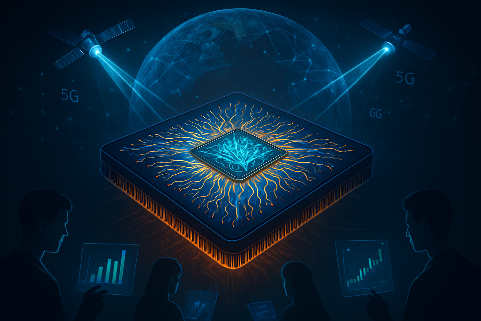
    As of October 2025, the global telecommunications industry stands on the precipice of a monumental shift, with the foundational research for 6G rapidly transitioning into critical development and prototyping phases. While commercial 6G deployment is still anticipated in the early 2030s, the immediate significance of this transition for the semiconductor industry cannot be overstated. Semiconductors are not merely components in the 6G equation; they are the indispensable architects, designing and fabricating the very fabric of the next-generation wireless world.

    The journey to 6G, promising unprecedented speeds of up to 1 terabit per second, near-zero latency, and the seamless integration of AI into every facet of connectivity, demands a revolution in chip technology. This pivotal moment, as standardization efforts commence and prototyping intensifies, places immense pressure and offers unparalleled opportunities for semiconductor manufacturers. The industry is actively engaged in developing advanced materials like Gallium Nitride (GaN) and Silicon Carbide (SiC) for high-frequency operations extending into the terahertz spectrum, pioneering innovative packaging solutions, and integrating AI chipsets directly into network infrastructure to manage the immense complexity and computational demands. The race to deliver high-performance, energy-efficient chips capable of enabling truly immersive digital experiences and autonomous systems is now, defining which nations and companies will lead the charge into the era of ubiquitous, intelligent connectivity.

    The Technical Imperative: Pushing the Boundaries of Silicon

    The Sixth Generation (6G) of wireless communication is poised to revolutionize connectivity by pushing the boundaries of existing technologies, aiming for unprecedented data rates, ultra-low latency, and pervasive intelligence. This ambitious leap necessitates significant innovations in semiconductor technology, differing markedly from the demands of its predecessor, 5G.

    Specific Technical Demands of 6G

    6G networks are envisioned to deliver capabilities far beyond 5G, enabling applications such as real-time analytics for smart cities, remote-controlled robotics, advanced healthcare diagnostics, holographic communications, extended reality (XR), and tactile internet. To achieve this, several key technical demands must be met:

    • Higher Frequencies (mmWave, sub-THz, THz): While 5G pioneered the use of millimeter-wave (mmWave) frequencies (24-100 GHz), 6G will extensively explore and leverage even higher frequency bands, specifically sub-terahertz (sub-THz) and terahertz (THz) ranges. The THz band is defined as frequencies from 0.1 THz up to 10 THz. Higher frequencies offer vast untapped spectrum and extremely high bandwidths, crucial for ultra-high data rates, but are more susceptible to significant path loss and atmospheric absorption. 6G will also utilize a "workhorse" cmWave spectrum (7-15 GHz) for broad coverage.
    • Increased Data Rates: 6G aims for peak data rates in the terabit per second (Tbps) range, with some projections suggesting up to 1 Tbps, a 100-fold increase over 5G's targeted 10 Gbps.
    • Extreme Low Latency and Enhanced Reliability: 6G targets latency less than 0.1 ms (a 100-fold increase over 5G) and network dependability of 99.99999%, enabling real-time human-machine interaction.
    • New Communication Paradigms: 6G will integrate novel communication concepts:
      • AI-Native Air Interface: AI and Machine Learning (ML) will be intrinsically integrated, enabling intelligent resource allocation, network optimization, and improved energy efficiency.
      • Integrated Sensing and Communication (ISAC): 6G will combine sensing and communication, allowing the network to transmit data and sense the physical environment for applications like holographic digital twins.
      • Holographic Communication: This paradigm aims to enable holographic projections and XR by simultaneously transmitting multiple data streams.
      • Reconfigurable Intelligent Surfaces (RIS): RIS are passive controllable surfaces that can dynamically manipulate radio waves to shape the radio environment, enhancing coverage and range of high-frequency signals.
      • Non-Terrestrial Networks (NTN): 6G will integrate aerial connectivity (LEO satellites, HAPS, UAVs) for ubiquitous coverage.

    Semiconductor Innovations for 6G

    Meeting these extreme demands requires substantial advancements in semiconductor technology, pushing beyond the limits of traditional silicon scaling.

    • Materials:
      • Gallium Nitride (GaN): Critical for high-frequency performance and power handling, enabling faster, more reliable communication. Innovations include GaN-based device architectures like Superlattice Castellated Field Effect Transistors (SLCFETs) for W-band operations.
      • Indium Phosphide (InP) and Silicon-Germanium (SiGe): Explored for sub-THz operations (500-1000 GHz and beyond 1 THz) for power amplifiers (PAs) and low-noise amplifiers (LNAs).
      • Advanced CMOS: While challenged by high voltages, CMOS remains viable for 6G's multi-antenna systems due to reduced transmit power requirements.
      • 2D Materials (e.g., graphene) and Wide-Bandgap (WBG) Semiconductors (GaN, SiC): Indispensable for power electronics in 5G/6G infrastructure and data centers due to their efficiency.
      • Liquid Crystals (LC): Being developed for RIS as an energy-efficient, scalable alternative.
    • Architectures:
      • Heterogeneous Integration and Chiplets: Advanced packaging and chiplet technology are crucial. Chiplets, specialized ICs, are interconnected within a single package, allowing for optimal process node utilization and enhanced performance. A new chip prototype integrates photonic components into a conventional electronic-based circuit board using chiplets for high-frequency 6G networks.
      • Advanced Packaging (2.5D, 3D ICs, Fan-out, Antenna-in-Package): Essential for miniaturization and performance. 2.5D and 3D packaging are critical for High-Performance Computing (HPC). Fan-out packaging is used for application processors and 5G/6G modem chips. Antenna-in-package (AiP) technology addresses signal loss and heat management in high-frequency systems.
      • AI Accelerators: Specialized AI hardware (GPUs, ASICs, NPUs) will handle the immense computational demands of 6G's AI-driven applications.
      • Energy-Efficient Designs: Efforts focus on breakthroughs in energy-efficient architectures to manage projected power requirements.
    • Manufacturing Processes:
      • Extreme Ultraviolet (EUV) Lithography: Continued miniaturization for next-generation logic at 2nm nodes and beyond.
      • Gate-All-Around FET (GAAFET) Transistors: Succeeding FinFET, GAAFETs enhance electrostatic control for more powerful and energy-efficient processors.
      • Wafer-Level Packaging: Allows for single-digit micrometer interconnect pitches and high bandwidths.

    How This Differs from 5G and Initial Reactions

    The shift from 5G to 6G represents a radical upgrade in semiconductor technology. While 5G primarily uses sub-6 GHz and mmWave (24-100 GHz), 6G significantly expands into sub-THz and THz bands (above 100 GHz). 5G aims for peak speeds of around 10 Gbps; 6G targets Tbps-level. 6G embeds AI as a fundamental component and introduces concepts like ISAC, holographic communication, and RIS as core enablers, which were not central to 5G's initial design. The complexity of 5G's radio interface led to a nearly 200-fold increase in processing needs over 4G LTE, and 6G will demand even more advanced semiconductor processes.

    The AI research community and industry experts have responded positively to the vision of 6G, recognizing the strategic importance of integrating advanced AI with semiconductor innovation. There's strong consensus that AI will be an indispensable tool for 6G, optimizing complex wireless systems. However, experts acknowledge significant hurdles, including the high cost of infrastructure, technical complexity in achieving stable terahertz waves, power consumption, thermal management, and the need for global standardization. The industry is increasingly focused on advanced packaging and novel materials as the "new battleground" for semiconductor innovation.

    Industry Tectonic Plates Shift: Impact on Tech Giants and Innovators

    The advent of 6G technology, anticipated to deliver speeds up to 100 times faster than 5G (reaching 1 terabit per second) and near-zero latency of 0.1 milliseconds, is set to profoundly reshape the semiconductor industry and its various players. This next-generation wireless communication standard will integrate AI natively, operate on terahertz (THz) frequencies, and enable a fully immersive and intelligent digital world, driving unprecedented demand for advanced semiconductor innovations.

    Impact on Industry Players

    6G's demanding performance requirements will ignite a significant surge in demand for cutting-edge semiconductors, benefiting established manufacturers and foundry leaders.

    • Major Semiconductor Manufacturers:
      • Advanced Process Nodes: Companies like Taiwan Semiconductor Manufacturing Company (TSMC: TSM) and Samsung Electronics Co., Ltd. (SMSN.L) stand to benefit from the demand for sub-5nm and even 3nm process nodes.
      • RF Components: Companies specializing in high-frequency RF front-end modules (RF FEMs), power amplifiers (PAs), and filters, such as Qualcomm Incorporated (QCOM), Broadcom Inc. (AVGO), Skyworks Solutions Inc. (SWKS), and Qorvo Inc. (QRVO), will see increased demand.
      • New Materials and Packaging: GlobalFoundries Inc. (GFS), through its partnership with Raytheon Technologies, is making strides in GaN-on-Si RF technology. MACOM Technology Solutions Holdings Inc (MTSI) also has direct exposure to GaN technology.
      • AI Accelerators and Specialized Processing: NVIDIA Corporation (NVDA), with its AI-driven simulation platforms and superchips, is strategically positioned. Intel Corporation (INTC) is also investing heavily in AI and 6G. Qualcomm (QCOM)'s Cloud AI 100 Ultra processor is designed for AI inferencing.
    • Network Equipment Providers: Companies like Ericsson (ERIC), Nokia Corporation (NOK), Huawei Technologies Co., Ltd. (private), ZTE Corporation (000063.SZ / 0763.HK), and Cisco Systems, Inc. (CSCO) are key players investing in 6G R&D, requiring advanced semiconductor components for new base stations and core network infrastructure.
    • AI Companies and Tech Giants:
      • AI Chip Designers: NVIDIA (NVDA), Advanced Micro Devices, Inc. (AMD), and Qualcomm (QCOM) will see their AI-specific chips become indispensable.
      • Tech Giants Leveraging AI and 6G: Google (GOOGL) and Microsoft Corporation (MSFT) will benefit for cloud services and distributed AI. Apple Inc. (AAPL) and Meta Platforms, Inc. (META) will leverage 6G for immersive AR/VR experiences. Amazon.com, Inc. (AMZN) could leverage 6G for AWS cloud computing and autonomous systems.
    • Startups: Opportunities exist in niche semiconductor solutions, novel materials, advanced packaging, specialized AI algorithms for 6G, and disruptive use cases like advanced mixed reality.

    Competitive Implications and Potential Disruption

    The 6G era will intensify competition, particularly in the race for AI-native infrastructure and ecosystem control. Tech giants will vie for dominance across the entire 6G stack, leading to increased custom silicon design. The massive data generated by 6G will further fuel the competitive advantage of companies that can effectively leverage it for AI. Geopolitical factors, such as US sanctions impacting China's access to advanced lithography, could also foster technological sovereignty.

    Disruptions will be significant: the metaverse and XR will be transformed, real-time remote operations will become widespread in healthcare and manufacturing, and a truly pervasive Internet of Things (IoT) will emerge. Telecommunication companies have an opportunity to move beyond being "data pipes" and generate new value from enhanced connectivity and AI-driven services.

    Market Positioning and Strategic Advantages

    Companies are adopting several strategies: early R&D investment (e.g., Samsung (SMSN.L), Huawei, Intel (INTC)), strategic partnerships, differentiation through specialized solutions, and leveraging AI-driven design and optimization tools (e.g., Synopsys (SNPS), Cadence Design Systems (CDNS)). The push for open networks and hardware-software disaggregation offers more choices, while a focus on energy efficiency presents a strategic advantage. Government funding and policies, such as India's Semiconductor Mission, also play a crucial role in shaping market positioning.

    A New Digital Epoch: Wider Significance and Societal Shifts

    The convergence of 6G telecommunications and advanced semiconductor innovations is poised to usher in a transformative era, profoundly impacting the broader AI landscape and society at large. As of October 2025, while 5G continues its global rollout, extensive research and development are already shaping the future of 6G, with commercial availability anticipated around 2030.

    Wider Significance of 6G

    6G networks are envisioned to be a significant leap beyond 5G, offering unprecedented capabilities, including data rates potentially reaching 1 terabit per second (Tbps), ultra-low latency measured in microseconds (down to 0.1 ms), and a massive increase in device connectivity, supporting up to 10 million devices per square kilometer. This represents a 10 to 100 times improvement over 5G in capacity and speed.

    New applications and services enabled by 6G will include:

    • Holographic Telepresence and Immersive Experiences: Enhancing AR/VR to create fully immersive metaverse experiences.
    • Autonomous Systems and Industry 4.0: Powering fully autonomous vehicles, robotic factories, and intelligent drones.
    • Smart Cities and IoT: Facilitating hyper-connected smart cities with real-time monitoring and autonomous public transport.
    • Healthcare Innovations: Enabling remote surgeries, real-time diagnostics, and unobtrusive health monitoring.
    • Integrated Sensing and Communication (ISAC): Turning 6G networks into sensors for high-precision target perception and smart traffic management.
    • Ubiquitous Connectivity: Integrating satellite-based networks for global coverage, including remote and underserved areas.

    Semiconductor Innovations

    Semiconductor advancements are foundational to realizing the potential of 6G and advanced AI. The industry is undergoing a profound transformation, driven by an "insatiable appetite" for computational power. Key innovations as of 2025 and anticipated future trends include:

    • Advanced Process Nodes: Development of 3nm and 2nm manufacturing nodes.
    • 3D Stacking (3D ICs) and Advanced Packaging: Vertically integrating multiple semiconductor dies to dramatically increase compute density and reduce latency.
    • Novel Materials: Exploration of GaN and SiC for power electronics, and 2D materials like graphene for future applications.
    • AI Chips and Accelerators: Continued development of specialized AI-focused processors. The AI chip market is projected to exceed $150 billion in 2025.
    • AI in Chip Design and Manufacturing: AI-powered Electronic Design Automation (EDA) tools automate tasks and optimize chip design, while AI improves manufacturing efficiency.

    Fit into the Broader AI Landscape and Trends

    6G and advanced semiconductor innovations are inextricably linked with the evolution of AI, creating a powerful synergy:

    • AI-Native Networks: 6G is designed to be AI-native, with AI/ML at its core for network optimization and intelligent automation.
    • Edge AI and Distributed AI: Ultra-low latency and massive connectivity enable widespread Edge AI, running AI models directly on local devices, leading to faster responses and enhanced privacy.
    • Pervasive and Ubiquitous AI: The seamless integration of communication, sensing, computation, and intelligence will lead to AI embedded in every aspect of daily life.
    • Digital Twins: 6G will support highly accurate digital twins for advanced manufacturing and smart cities.
    • AI for 6G and 6G for AI: AI will enable 6G by optimizing network functions, while 6G will further advance AI/ML by efficiently transporting algorithms and exploiting local data.

    Societal Impacts

    The combined forces of 6G and semiconductor advancements will bring significant societal transformations: enhanced quality of life, economic growth and new industries, smart environments, and immersive human experiences. The global semiconductor market is projected to exceed $1 trillion by 2030, largely fueled by AI.

    Potential Concerns

    Alongside the benefits, there are several critical concerns:

    • Energy Consumption: Both 6G infrastructure and AI systems require massive power, exacerbating the climate crisis.
    • Privacy and Data Security: Hyper-connectivity and pervasive AI raise significant privacy and security concerns, requiring robust quantum-resistant cryptography.
    • Digital Divide: While 6G can bridge divides, there's a risk of exacerbating inequalities if access remains uneven or unaffordable.
    • Ethical Implications and Job Displacement: Increasing AI autonomy raises ethical questions and potential job displacement.
    • Geopolitical Tensions and Supply Chain Vulnerabilities: These factors increase costs and hinder innovation, fostering a push for technological sovereignty.
    • Technological Fragmentation: Geopolitical factors could lead to technology blocks, negatively impacting scalability and internationalization.

    Comparisons to Previous Milestones

    • 5G Rollout: 6G represents a transformative shift, not just an enhancement. It aims for speeds hundreds or thousands of times faster and near-zero latency, with AI being fundamentally native.
    • Early Internet: Similar to the early internet, 6G and AI are poised to be general-purpose technologies that can drastically alter societies and economies, fusing physical and digital worlds.
    • Early AI Milestones: The current AI landscape, amplified by 6G and advanced semiconductors, emphasizes distributed AI, edge computing, and real-time autonomous decision-making on a massive scale, moving from "connected things" to "connected intelligence."

    As of October 2025, 6G is still in the research and development phase, with standardization expected to begin in 2026 and commercial availability around 2030. The ongoing advancements in semiconductors are critical to overcoming the technical challenges and enabling the envisioned capabilities of 6G and the next generation of AI.

    The Horizon Beckons: Future Developments in 6G and Semiconductors

    The sixth generation of wireless technology, 6G, and advancements in semiconductor technology are poised to bring about transformative changes across various industries and aspects of daily life. These developments, driven by increasing demands for faster, more reliable, and intelligent systems, are progressing on distinct but interconnected timelines.

    6G Technology Developments

    The journey to 6G is characterized by ongoing research, standardization efforts, and the gradual introduction of advanced capabilities that build upon 5G.

    Near-Term Developments (Next 1-3 years from October 9, 2025, up to October 2028):

    • Standardization and Research Focus: The pre-standardization phase is underway, with 3GPP initiating requirement-related work in Release 19 (2024). The period until 2026 is dedicated to defining technical performance requirements. Early proof-of-concept demonstrations are expected.
    • Key Technological Focus Areas: R&D will concentrate on network resilience, AI-Radio Access Network (AI-RAN), generative AI, edge computing, advanced RF utilization, sensor fusion, immersive services, digital twins, and sustainability.
    • Spectrum Exploration: Initial efforts focus on leveraging the FR3 spectrum (centimeter wave) and new spectrum in the centimetric range (7-15 GHz).
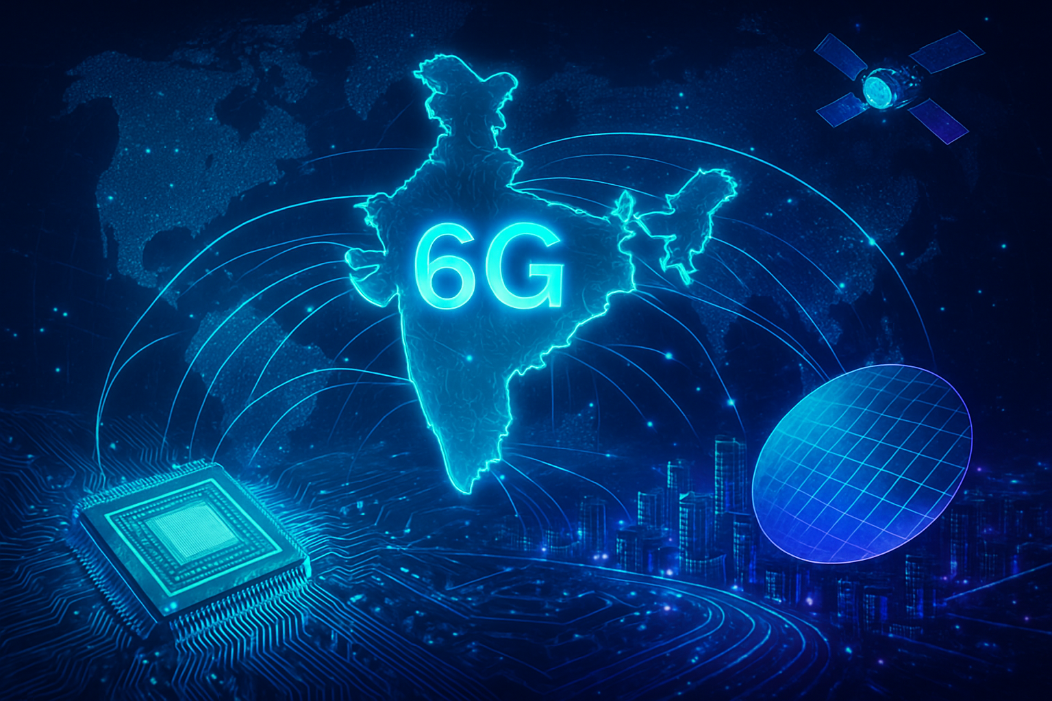
    • Early Trials and Government Initiatives: South Korea aims to commercialize initial 6G services by 2028. India has also launched multiple 6G research initiatives.

    Long-Term Developments (Beyond 2028):

    • Commercial Deployment: Commercial 6G services are widely anticipated around 2030, with 3GPP Release 21 specifications expected by 2028.
    • Ultra-High Performance: 6G networks are expected to achieve data speeds up to 1 Tbps and ultra-low latency.
    • Cyber-Physical World Integration: 6G will facilitate a seamless merger of the physical and digital worlds, involving ultra-lean design, limitless connectivity, and integrated sensing and communication.
    • AI-Native Networks: AI and ML will be deeply integrated into network operation and management for optimization and intelligent automation.
    • Enhanced Connectivity: 6G will integrate with satellite, Wi-Fi, and other non-terrestrial networks for ubiquitous global coverage.

    Potential Applications and Use Cases:

    6G is expected to unlock a new wave of applications:

    • Immersive Extended Reality (XR): High-fidelity AR/VR/MR experiences transforming gaming, education, and remote collaboration.
    • Holographic Communication: Realistic three-dimensional teleconferencing.
    • Autonomous Mobility: Enhanced support for autonomous vehicles with real-time environmental information.
    • Massive Digital Twinning: Real-time digital replicas of physical objects or environments.
    • Massive Internet of Things (IoT) Deployments: Support for billions of connected devices with ultra-low power consumption.
    • Integrated Sensing and Communication (ISAC): Networks gathering environmental information for new services like high-accuracy location.
    • Advanced Healthcare: Redefined telemedicine and AI-driven diagnostics.
    • Beyond-Communication Services: Exposing network, positioning, sensing, AI, and compute services to third-party developers.
    • Quantum Communication: Potential integration of quantum technologies for secure, high-speed channels.

    Challenges for 6G:

    • Spectrum Allocation: Identifying and allocating suitable THz frequency bands, which suffer from significant absorption.
    • Technological Limitations: Developing efficient antennas and network components for ultra-high data rates and ultra-low latency.
    • Network Architecture and Integration: Managing complex heterogeneous networks and developing new protocols.
    • Energy Efficiency and Sustainability: Addressing the increasing energy consumption of wireless networks.
    • Security and Privacy: New vulnerabilities from decentralized, AI-driven 6G, requiring advanced encryption and AI-driven threat detection.
    • Standardization and Interoperability: Achieving global consensus on technical standards.
    • Cost and Infrastructure Deployment: Significant investments required for R&D and deploying new infrastructure.
    • Talent Shortage: A critical shortage of professionals with combined expertise in wireless communication and AI.

    Semiconductor Technology Developments

    The semiconductor industry, the backbone of modern technology, is undergoing rapid transformation driven by the demands of AI, 5G/6G, electric vehicles, and quantum computing.

    Near-Term Developments (Next 1-3 years from October 9, 2025, up to October 2028):

    • AI-Driven Chip Design and Manufacturing: AI and ML are significantly driving the demand for faster, more efficient chips. AI-driven tools are expected to revolutionize chip design and verification, dramatically compressing development cycles. AI will also transform manufacturing optimization through predictive maintenance, defect detection, and real-time process control in fabrication plants.
    • Advanced Materials and Architectures: Expect continued innovation in wide-bandgap (WBG) materials like Silicon Carbide (SiC) and Gallium Nitride (GaN), with increased production, improved yields, and reduced costs. These are crucial for high-power applications in EVs, fast charging, renewables, and data centers.
    • Advanced Packaging and Memory: Chiplets, 3D ICs, and advanced packaging techniques (e.g., CoWoS/SoIC) are becoming standard for high-performance computing (HPC) and AI applications, with capacity expanding aggressively.
    • Geopolitical and Manufacturing Shifts: Governments are actively investing in domestic semiconductor manufacturing, with new fabrication facilities by TSMC (TSM), Intel (INTC), and Samsung (SMSN.L) expected to begin operations and expand in the US between 2025 and 2028. India is also projected to approve more semiconductor fabs in 2025.
    • Market Growth: The global semiconductor market is projected to reach approximately $697 billion in 2025, an 11% year-over-year increase, primarily driven by strong demand in data centers and AI technologies.
    • Automotive Sector Growth: The automotive semiconductor market is expected to outperform the broader industry, with an 8-9% compound annual growth rate (CAGR) from 2025 to 2030.
    • Edge AI and Specialized Chips: AI-capable PCs are projected to account for about 57% of shipments in 2026, and over 400 million GenAI smartphones are expected in 2025. There will be a rise in specialized AI chips tailored for specific applications.

    Long-Term Developments (Beyond 2028):

    • Trillion-Dollar Market: The semiconductor market is forecast to reach a $1 trillion valuation by 2030.
    • Autonomous Manufacturing: The vision includes fully autonomous manufacturing facilities and AI-designed chips with minimal human intervention.
    • Modular and Heterogeneous Computing: Fully modular semiconductor designs with custom chiplets optimized for specific AI workloads will dominate. There will be a significant transition from 2.5D to more prevalent 3D heterogeneous computing, and co-packaged optics (CPO) are expected to replace traditional copper interconnects.
    • New Materials and Architectures: Graphene and other two-dimensional (2D) materials are promising alternatives to silicon, helping to overcome the physical limits of traditional silicon technology. New architectures like Gate-All-Around FETs (GAA-FETs) and Complementary FETs (CFETs) will enable denser, more energy-efficient chips.
    • Integration with Quantum and Photonics: Further miniaturization and integration with quantum computing and photonics.
    • Techno-Nationalism and Diversification: Geopolitical tensions will likely solidify a deeply bifurcated global semiconductor market.

    Potential Applications and Use Cases:

    Semiconductor innovations will continue to power and enable new technologies across virtually every sector: AI and High-Performance Computing, autonomous systems, 5G/6G Communications, healthcare and biotechnology, Internet of Things (IoT) and smart environments, renewable energy, flexible and wearable electronics, environmental monitoring, space exploration, and optoelectronics.

    Challenges for Semiconductor Technology:

    • Increasing Complexity and Cost: The continuous shrinking of technology nodes makes chip design and manufacturing processes increasingly intricate and expensive.
    • Supply Chain Vulnerability and Geopolitical Tensions: The global and highly specialized nature of the semiconductor supply chain makes it vulnerable, leading to "techno-nationalism."
    • Talent Shortage: A severe and intensifying global shortage of skilled workers.
    • Technological Limits of Silicon: Silicon is approaching its inherent physical limits, driving the need for new materials and architectures.
    • Energy Consumption and Environmental Impact: The immense power demands of AI-driven data centers raise significant sustainability concerns.
    • Manufacturing Optimization: Issues such as product yield, quality control, and cost optimization remain critical.
    • Legacy Systems Integration: Many companies struggle with integrating legacy systems and data silos.

    Expert Predictions:

    Experts predict that the future of both 6G and semiconductor technologies will be deeply intertwined with artificial intelligence. For 6G, AI will be integral to network optimization, predictive maintenance, and delivering personalized experiences. In semiconductors, AI is not only a primary driver of demand but also a tool for accelerating chip design, verification, and manufacturing optimization. The global semiconductor market is expected to continue its robust growth, reaching $1 trillion by 2030, with specialized AI chips and advanced packaging leading the way. While commercial 6G deployment is still some years away (early 2030s), the strategic importance of 6G for technological, economic, and geopolitical power means that countries and coalitions are actively pursuing leadership.

    A New Era of Intelligence and Connectivity: The 6G-Semiconductor Nexus

    The advent of 6G technology, inextricably linked with groundbreaking advancements in semiconductors, promises a transformative leap in connectivity, intelligence, and human-machine interaction. This wrap-up consolidates the pivotal discussions around the challenges and opportunities at this intersection, highlighting its profound implications for AI and telecommunications.

    Summary of Key Takeaways

    The drive towards 6G is characterized by ambitions far exceeding 5G, aiming for ultra-fast data rates, near-zero latency, and massive connectivity. Key takeaways from this evolving landscape include:

    • Unprecedented Performance Goals: 6G aims for data rates reaching terabits per second (Tbps), with latency as low as 0.1 milliseconds (ms), a significant improvement over 5G's capabilities.
    • Deep Integration of AI: 6G networks will be "AI-native," relying on AI and machine learning (ML) to optimize resource allocation, predict network demand, and enhance security.
    • Expanded Spectrum Utilization: 6G will move into higher radio frequencies, including sub-Terahertz (THz) and potentially up to 10 THz, requiring revolutionary hardware.
    • Pervasive Connectivity and Sensing: 6G envisions merging diverse communication platforms (aerial, ground, sea, space) and integrating sensing, localization, and communication.
    • Semiconductors as the Foundation: Achieving 6G's goals is contingent upon radical upgrades in semiconductor technology, including new materials like Gallium Nitride (GaN), advanced process nodes, and innovative packaging technologies.
    • Challenges: Significant hurdles remain, including the enormous cost of building 6G infrastructure, resolving spectrum allocation, achieving stable terahertz waves, and ensuring robust cybersecurity.

    Significance in AI History and Telecommunications

    The development of 6G and advanced semiconductors marks a pivotal moment in both AI history and telecommunications:

    • For AI History: 6G represents the necessary infrastructure for the next generation of AI. Its ultra-low latency and massive capacity will enable real-time, on-device AI applications, shifting processing to the network edge. This "Network for AI" paradigm will allow the proliferation of personal AI helpers and truly autonomous, cognitive networks.
    • For Telecommunications: 6G is a fundamental transformation, redefining network operation into a self-managing, cognitive platform. It will enable highly personalized services, real-time network assurance, and immersive user experiences, fostering new revenue opportunities. The integration of AI will allow networks to dynamically adjust to customer needs and manage dense IoT deployments.

    Final Thoughts on Long-Term Impact

    The long-term impact of 6G and advanced semiconductors will be profound and far-reaching:

    • Hyper-Connected, Intelligent Societies: Smart cities, autonomous vehicles, and widespread digital twin models will become a reality.
    • Revolutionized Healthcare: Remote diagnostics, real-time remote surgery, and advanced telemedicine will become commonplace.
    • Immersive Human Experiences: Hyper-realistic extended reality (AR/VR/MR) and holographic communications will become seamless.
    • Sustainability and Energy Efficiency: Energy efficiency will be a major design criterion for 6G, optimizing energy consumption across components.
    • New Economic Paradigms: The convergence will drive Industry 5.0, enabling new business models and services, with the semiconductor market projected to surpass $1 trillion by 2030.

    What to Watch For in the Coming Weeks and Months (from 10/9/2025)

    The period between late 2025 and 2026 is critical for the foundational development of 6G:

    • Standardization Progress: Watch for initial drafts and discussions from the ITU-R and 3GPP that will define the core technical specifications for 6G.
    • Semiconductor Breakthroughs: Expect announcements regarding new chip prototypes and manufacturing processes, particularly addressing higher frequencies and power efficiency. The semiconductor industry is already experiencing strong growth in 2025, projected to reach $700.9 billion.
    • Early Prototypes and Trials: Look for demonstrations of 6G capabilities in laboratory or limited test environments, focusing on sub-THz communication, integrated sensing, and AI-driven network management. Qualcomm (QCOM) anticipates pre-commercial 6G devices as early as 2028.
    • Government Initiatives and Funding: Monitor announcements from governments and alliances (like the EU's Hexa-X and the US Next G Alliance) regarding research grants and roadmaps for 6G development. South Korea's $325 million 6G development plan in 2025 is a prime example.
    • Addressing Challenges: Keep an eye on progress in addressing critical challenges such as efficient power management for higher frequencies, enhanced security solutions including post-quantum cryptography, and strategies to manage the massive data generated by 6G networks.

    The journey to 6G is a complex but exhilarating one, promising to redefine our digital existence. The coming months will be crucial for laying the groundwork for a truly intelligent and hyper-connected future.


    This content is intended for informational purposes only and represents analysis of current AI developments.

    TokenRing AI delivers enterprise-grade solutions for multi-agent AI workflow orchestration, AI-powered development tools, and seamless remote collaboration platforms.
    For more information, visit https://www.tokenring.ai/.

  • India’s 6G Leap: A $1.2 Trillion Bet on Semiconductors and Global Leadership

    India’s 6G Leap: A $1.2 Trillion Bet on Semiconductors and Global Leadership

    India is embarking on an ambitious journey to establish itself as a global leader in next-generation telecommunications through its "Bharat 6G Mission." Unveiled in March 2023, this strategic initiative aims to not only revolutionize connectivity within the nation but also position India as a net exporter of 6G technology and intellectual property by 2030. At the heart of this colossal undertaking lies a critical reliance on advanced semiconductor technology, with the mission projected to inject a staggering $1.2 trillion into India's Gross Domestic Product (GDP) by 2035.

    The mission's immediate significance lies in its dual focus: fostering indigenous innovation in advanced wireless communication and simultaneously building a robust domestic semiconductor ecosystem. Recognizing that cutting-edge 6G capabilities are inextricably linked to sophisticated chip design and manufacturing, India is strategically investing in both domains. This integrated approach seeks to reduce reliance on foreign technology, enhance national security in critical infrastructure, and unlock unprecedented economic growth across diverse sectors, from smart cities and healthcare to agriculture and disaster management.

    Pushing the Boundaries: Technical Ambitions and Silicon Foundations

    India's Bharat 6G Vision outlines a comprehensive roadmap for pushing the technological envelope far beyond current 5G capabilities. The mission targets several groundbreaking areas, including Terahertz (THz) communication, which promises ultra-high bandwidth and extremely low latency; the integration of artificial intelligence (AI) for linked intelligence and network optimization; the development of a tactile internet for real-time human-machine interaction; and novel encoding methods, waveform chipsets, and ultra-precision networking. Furthermore, the initiative encompasses mobile communications in space, including the crucial integration of Low Earth Orbit (LEO) satellites to ensure pervasive connectivity.

    A cornerstone of achieving these advanced 6G capabilities is the parallel development of India's semiconductor industry. The government has explicitly linked research proposals for 6G to advancements in semiconductor design. The "Made-in-India" chip initiative, spearheaded by the India Semiconductor Mission (ISM) with a substantial budget of ₹75,000 Crore (approximately $9 billion USD), aims to make India a global hub for semiconductor manufacturing and design. Prime Minister Narendra Modi's announcement that India's first homegrown semiconductor chip is anticipated by the end of 2025 underscores the urgency and strategic importance placed on this sector. This domestic chip production is not merely about self-sufficiency; it's about providing the custom silicon necessary to power the complex demands of 6G networks, AI processing, IoT devices, and smart infrastructure, fundamentally differentiating India's approach from previous generations of telecom development.

    Initial reactions from the AI research community and industry experts, both domestically and internationally, have been largely positive, recognizing the strategic foresight of linking 6G with semiconductor independence. The establishment of the Technology Innovation Group on 6G (TIG-6G) by the Department of Telecommunications (DoT) and the subsequent launch of the Bharat 6G Alliance (B6GA) in July 2023, bringing together public, private, academic, and startup entities, signifies a concerted national effort. These bodies are tasked with identifying key research areas, fostering interdisciplinary collaboration, advising on policy, and driving the design, development, and deployment of 6G technologies, aiming for India to secure 10% of global 6G patents by 2027.

    Reshaping the Tech Landscape: Corporate Beneficiaries and Competitive Edge

    The ambitious Bharat 6G Mission, coupled with a robust domestic semiconductor push, is poised to significantly reshape the landscape for a multitude of companies, both within India and globally. Indian telecom giants like Reliance Jio Infocomm Limited (NSE: JIOFIN), Bharti Airtel Limited (NSE: AIRTEL), and state-owned Bharat Sanchar Nigam Limited (BSNL) stand to be primary beneficiaries, moving from being mere consumers of telecom technology to active developers and exporters. These companies will play crucial roles in field trials, infrastructure deployment, and the eventual commercial rollout of 6G services.

    Beyond the telecom operators, the competitive implications extend deeply into the semiconductor and AI sectors. Indian semiconductor startups and established players, supported by the India Semiconductor Mission, will see unprecedented opportunities in designing and manufacturing specialized chips for 6G infrastructure, AI accelerators, and edge devices. This could potentially disrupt the dominance of established global semiconductor manufacturers by fostering a new supply chain originating from India. Furthermore, AI research labs and startups will find fertile ground for innovation, leveraging 6G's ultra-low latency and massive connectivity to develop advanced AI applications, from real-time analytics for smart cities to remote-controlled robotics and advanced healthcare diagnostics.

    The mission also presents a strategic advantage for India in global market positioning. By aiming to contribute significantly to 6G standards and intellectual property, India seeks to reduce its reliance on foreign technology vendors, a move that could shift the balance of power in the global telecom equipment market. Companies that align with India's indigenous development goals, including international partners willing to invest in local R&D and manufacturing, are likely to gain a competitive edge. This strategic pivot could lead to a new wave of partnerships and joint ventures, fostering a collaborative ecosystem while simultaneously strengthening India's technological sovereignty.

    Broadening Horizons: A Catalyst for National Transformation

    India's 6G mission is more than just a technological upgrade; it represents a profound national transformation initiative that integrates deeply with broader AI trends and the nation's digital aspirations. By aiming for global leadership in 6G, India is positioning itself at the forefront of the next wave of digital innovation, where AI, IoT, and advanced connectivity converge. This fits seamlessly into the global trend of nations vying for technological self-reliance and leadership in critical emerging technologies. The projected $1.2 trillion contribution to GDP by 2035 underscores the government's vision of 6G as a powerful economic engine, driving productivity and innovation across every sector.

    The impacts of this mission are far-reaching. In agriculture, 6G-enabled precision farming, powered by AI and IoT, could optimize yields and reduce waste. In healthcare, ultra-reliable low-latency communication could facilitate remote surgeries and real-time patient monitoring. Smart cities will become truly intelligent, with seamlessly integrated sensors and AI systems managing traffic, utilities, and public safety. However, potential concerns include the immense capital investment required for R&D and infrastructure, the challenge of attracting and retaining top-tier talent in both semiconductor and 6G domains, and navigating the complexities of international standardization and geopolitical competition. Comparisons to previous milestones, such as India's success in IT services and digital public infrastructure (e.g., Aadhaar, UPI), highlight the nation's capacity for large-scale digital transformation, but 6G and semiconductor manufacturing present a new level of complexity and capital intensity.

    This initiative signifies India's intent to move beyond being a consumer of technology to a significant global innovator and provider. It's a strategic move to secure a prominent position in the future digital economy, ensuring that the country has a strong voice in shaping the technological standards and intellectual property that will define the next few decades. The emphasis on affordability, sustainability, and ubiquity in its 6G solutions also suggests a commitment to inclusive growth, aiming to bridge digital divides and ensure widespread access to advanced connectivity.

    The Road Ahead: Anticipated Innovations and Persistent Challenges

    The journey towards India's 6G future is structured across a clear timeline, with significant developments expected in the near and long term. Phase I (2023-2025) is currently focused on exploratory research, proof-of-concept testing, and identifying innovative pathways, including substantial investments in R&D for terahertz communication, quantum networks, and AI-optimized protocols. This phase also includes the establishment of crucial 6G testbeds, laying the foundational infrastructure for future advancements. The anticipation of India's first homegrown semiconductor chip by the end of 2025 marks a critical near-term milestone that will directly impact the pace of 6G development.

    Looking further ahead, Phase II (2025-2030) will be dedicated to intensive intellectual property creation, the deployment of large-scale testbeds, comprehensive trials, and fostering international collaborations. Experts predict that the commercial rollout of 6G services in India will commence around 2030, aligning with the International Mobile Telecommunications (IMT) 2030 standards, which are expected to be finalized by 2027-2028. Potential applications on the horizon include immersive holographic communications, hyper-connected autonomous systems (vehicles, drones), advanced robotic surgery with haptic feedback, and truly ubiquitous connectivity through integrated terrestrial and non-terrestrial networks (NTN).

    However, significant challenges remain. Scaling up indigenous semiconductor manufacturing capabilities, which is a capital-intensive and technologically complex endeavor, is paramount. Attracting and nurturing a specialized talent pool in both advanced wireless communication and semiconductor design will be crucial. Furthermore, India's ability to influence global 6G standardization efforts against established players will determine its long-term impact. Experts predict that while the vision is ambitious, India's concerted government support, academic engagement, and industry collaboration, particularly through the Bharat 6G Alliance and its international MoUs, provide a strong framework for overcoming these hurdles and realizing its goal of global 6G leadership.

    A New Dawn for Indian Tech: Charting the Future of Connectivity

    India's Bharat 6G Mission, intricately woven with its burgeoning semiconductor ambitions, represents a pivotal moment in the nation's technological trajectory. The key takeaways are clear: India is not merely adopting the next generation of wireless technology but actively shaping its future, aiming for self-reliance in critical components, and projecting a substantial economic impact of $1.2 trillion by 2035. This initiative signifies a strategic shift from being a technology consumer to a global innovator and exporter of cutting-edge telecom and semiconductor intellectual property.

    The significance of this development in AI history and the broader tech landscape cannot be overstated. By vertically integrating semiconductor manufacturing with 6G development, India is building a resilient and secure digital future. This approach fosters national technological sovereignty and positions the country as a formidable player in the global race for advanced connectivity. The long-term impact will likely be a more digitally empowered India, driving innovation across industries and potentially inspiring similar integrated technology strategies in other developing nations.

    In the coming weeks and months, observers should closely watch the progress of the India Semiconductor Mission, particularly the development and market availability of the first homegrown chips. Further activities and partnerships forged by the Bharat 6G Alliance, both domestically and internationally, will also be crucial indicators of the mission's momentum. The world will be watching as India endeavors to transform its vision of a hyper-connected, AI-driven future into a tangible reality, solidifying its place as a technological powerhouse on the global stage.

    This content is intended for informational purposes only and represents analysis of current AI developments.

    TokenRing AI delivers enterprise-grade solutions for multi-agent AI workflow orchestration, AI-powered development tools, and seamless remote collaboration platforms.
    For more information, visit https://www.tokenring.ai/.