As of January 28, 2026, the global race for artificial intelligence dominance is no longer being fought solely in the realm of algorithmic breakthroughs or raw transistor counts. Instead, the front line of the AI revolution has moved to a high-precision manufacturing stage known as "Advanced Packaging." At the heart of this struggle is Taiwan Semiconductor Manufacturing Company (TSMC) (NYSE: TSM), whose proprietary CoWoS (Chip on Wafer on Substrate) technology has become the single most critical bottleneck in the production of high-end AI accelerators. Despite a multi-billion dollar expansion blitz, the supply of CoWoS capacity remains "structurally oversubscribed," dictating the pace at which the world’s tech giants can deploy their next-generation models.
The immediate significance of this bottleneck cannot be overstated. In early 2026, the ability to secure CoWoS allocation is directly correlated with a company’s market valuation and its competitive standing in the AI landscape. While the industry has seen massive leaps in GPU architecture, those chips are useless without the high-bandwidth memory (HBM) integration that CoWoS provides. This technical "chokepoint" has effectively divided the tech world into two camps: those who have secured TSMC’s 2026 capacity—most notably NVIDIA (NASDAQ: NVDA)—and those currently scrambling for "second-source" alternatives or waiting in an 18-month-long production queue.
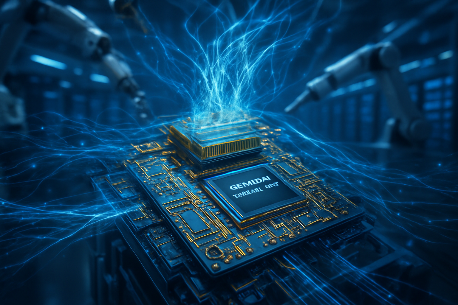
The Engineering of a Bottleneck: Inside the CoWoS Architecture
Technically, CoWoS is a 2.5D packaging technology that allows for the integration of multiple silicon dies—typically a high-performance logic GPU and several stacks of High-Bandwidth Memory (HBM4 in 2026)—onto a single, high-density interposer. Unlike traditional packaging, which connects a finished chip to a circuit board using relatively coarse wires, CoWoS creates microscopic interconnections that enable massive data throughput between the processor and its memory. This "memory wall" is the primary obstacle in training Large Language Models (LLMs); without the ultra-fast lanes provided by CoWoS, the world’s most powerful GPUs would spend the majority of their time idling, waiting for data.
In 2026, the technology has evolved into three distinct flavors to meet varying industry needs. CoWoS-S (Silicon) remains the legacy standard, using a monolithic silicon interposer that is now facing physical size limits. To break this "reticle limit," TSMC has pivoted aggressively toward CoWoS-L (Local Silicon Interconnect), which uses small silicon "bridges" embedded in an organic layer. This allows for massive packages up to 6 times the size of a standard chip, supporting up to 16 HBM4 stacks. Meanwhile, CoWoS-R (Redistribution Layer) offers a cost-effective organic alternative for high-speed networking chips from companies like Broadcom (NASDAQ: AVGO) and Cisco (NASDAQ: CSCO).
The reason scaling this technology is so difficult lies in its environmental and precision requirements. Advanced packaging now requires cleanroom standards that rival front-end wafer fabrication—specifically ISO Class 5 environments where fewer than 3,500 microscopic particles exist per cubic meter. Furthermore, the specialized tools required for this process, such as hybrid bonders from Besi and high-precision lithography tools from ASML (NASDAQ: ASML), currently have lead times exceeding 12 to 18 months. Even with TSMC’s massive $56 billion capital expenditure budget for 2026, the physical reality of building these ultra-clean facilities and waiting for precision equipment means that the supply-demand gap will not fully close until at least 2027.
A Two-Tiered AI Industry: Winners and Losers in the Capacity War
The scarcity of CoWoS capacity has created a stark divide in the corporate hierarchy. NVIDIA (NASDAQ: NVDA) remains the undisputed king of the hill, having used its massive cash reserves to pre-book approximately 60% of TSMC’s total 2026 CoWoS output. This strategic move has ensured that its Rubin and Blackwell Ultra architectures remain the dominant hardware for hyperscalers like Microsoft and Meta. For NVIDIA, CoWoS isn't just a technical spec; it is a defensive moat that prevents competitors from scaling their hardware even if they have superior designs on paper.
In contrast, other major players are forced to navigate a more precarious path. AMD (NASDAQ: AMD), while holding a respectable 11% allocation for its MI355 and MI400 series, has begun qualifying "second-source" packaging partners like ASE Group and Amkor to mitigate its reliance on TSMC. This diversification strategy is risky, as shifting packaging providers can impact yields and performance, but it is a necessary gamble in an environment where TSMC's "wafer starts per month" are spoken for years in advance. Meanwhile, custom silicon efforts from Google and Amazon (via Broadcom) occupy another 15% of the market, leaving startups and second-tier AI labs to fight over the remaining 14% of capacity, often at significantly higher "spot market" prices.
This dynamic has also opened a door for Intel (NASDAQ: INTC). Recognizing the bottleneck, Intel has positioned its "Foundry" business as a turnkey packaging alternative. In early 2026, Intel is pitching its EMIB (Embedded Multi-die Interconnect Bridge) and Foveros 3D packaging technologies to customers who may have their chips fabricated at TSMC but want to avoid the CoWoS waitlist. This "open foundry" model is Intel’s best chance at reclaiming market share, as it offers a faster time-to-market for companies that are currently "capacity-starved" by the TSMC logjam.
Geopolitics and the Shift from Moore’s Law to 'More than Moore'
The CoWoS bottleneck represents a fundamental shift in the semiconductor industry's philosophy. For decades, "Moore’s Law"—the doubling of transistors on a single chip—was the primary driver of progress. However, as we approach the physical limits of silicon atoms, the industry has shifted toward "More than Moore," an era where performance gains come from how chips are integrated and packaged together. In this new paradigm, the "packaging house" is just as strategically important as the "fab." This has elevated TSMC from a manufacturing partner to what analysts are calling a "Sovereign Utility of Computation."
This concentration of power in Taiwan has significant geopolitical implications. In early 2026, the "Silicon Shield" is no longer just about the chips themselves, but about the unique CoWoS lines in facilities like the new Chiayi AP7 plant. Governments around the world are now waking up to the fact that "Sovereign AI" requires not just domestic data centers, but a domestic advanced packaging supply chain. This has spurred massive subsidies in the U.S. and Europe to bring packaging capacity closer to home, though these projects are still years away from reaching the scale of TSMC’s Taiwanese operations.
The environmental and resource concerns of this expansion are also coming to the forefront. The high-precision bonding and thermal management required for CoWoS-L packages consume significant amounts of energy and ultrapure water. As TSMC scales to its target of 150,000 wafer starts per month by the end of 2026, the strain on Taiwan’s infrastructure has become a central point of debate, highlighting the fragile foundation upon which the global AI boom is built.
Beyond the Silicon Interposer: The Future of Integration
Looking past the current 2026 bottleneck, the industry is already preparing for the next evolution in integration: glass substrates. Intel has taken an early lead in this space, launching its first chips using glass cores in early 2026. Glass offers superior flatness and thermal stability compared to the organic materials currently used in CoWoS, potentially solving the "warpage" issues that plague the massive 6x reticle-sized chips of the future.
We are also seeing the rise of "System on Integrated Chips" (SoIC), a true 3D stacking technology that eliminates the interposer entirely by bonding chips directly on top of one another. While currently more expensive and difficult to manufacture than CoWoS, SoIC is expected to become the standard for the "Super-AI" chips of 2027 and 2028. Experts predict that the transition from 2.5D (CoWoS) to 3D (SoIC) will be the next major battleground, with Samsung (OTC: SSNLF) betting heavily on its "Triple Alliance" of memory, foundry, and packaging to leapfrog TSMC in the 3D era.
The challenge for the next 24 months will be yield management. As packages become larger and more complex, a single defect in one of the eight HBM stacks or the central GPU can ruin the entire multi-thousand-dollar assembly. The development of "repairable" or "modular" packaging techniques is a major area of research for 2026, as manufacturers look for ways to salvage these high-value components when a single connection fails during the bonding process.
Final Assessment: The Road Through 2026
The CoWoS bottleneck is the defining constraint of the 2026 AI economy. While TSMC’s aggressive capacity expansion is slowly beginning to bear fruit, the "insatiable" demand from NVIDIA and the hyperscalers ensures that advanced packaging will remain a seller’s market for the foreseeable future. We have entered an era where "computing power" is a physical commodity, and its availability is determined by the precision of a few dozen high-tech bonding machines in northern Taiwan.
As we move into the second half of 2026, watch for the ramp-up of Samsung’s Taylor, Texas facility and Intel’s ability to win over "CoWoS refugees." The successful mass production of glass substrates and the maturation of 3D SoIC technology will be the key indicators of who wins the next phase of the AI war. For now, the world remains tethered to TSMC's packaging lines—a microscopic bridge that supports the weight of the entire global AI industry.
This content is intended for informational purposes only and represents analysis of current AI developments.
TokenRing AI delivers enterprise-grade solutions for multi-agent AI workflow orchestration, AI-powered development tools, and seamless remote collaboration platforms.
For more information, visit https://www.tokenring.ai/.