As the AI revolution enters its most capital-intensive phase yet in early 2026, the industry’s greatest challenge is no longer just the design of smarter algorithms or the procurement of raw silicon. Instead, the global technology sector finds itself locked in a desperate scramble for "Advanced Packaging," specifically the Chip-on-Wafer-on-Substrate (CoWoS) technology pioneered by Taiwan Semiconductor Manufacturing Company (TSMC) (NYSE: TSM). While 2024 and 2025 were defined by the shortage of logic chips themselves, 2026 has seen the bottleneck shift entirely to the complex assembly process that binds massive compute dies to ultra-fast memory.
This specialized manufacturing step is currently the primary throttle on global AI GPU supply, dictating the pace at which tech giants can build the next generation of "Super-Intelligence" clusters. With TSMC's CoWoS lines effectively sold out through the end of the year and premiums for "hot run" priority reaching record highs, the ability to secure packaging capacity has become the ultimate competitive advantage. For NVIDIA (NASDAQ: NVDA), Advanced Micro Devices (NASDAQ: AMD), and the hyperscalers developing their own custom silicon, the battle for 2026 isn't being fought in the design lab, but on the factory floors of automated backend facilities in Taiwan.
The Technical Crucible: CoWoS-L and the HBM4 Integration Challenge
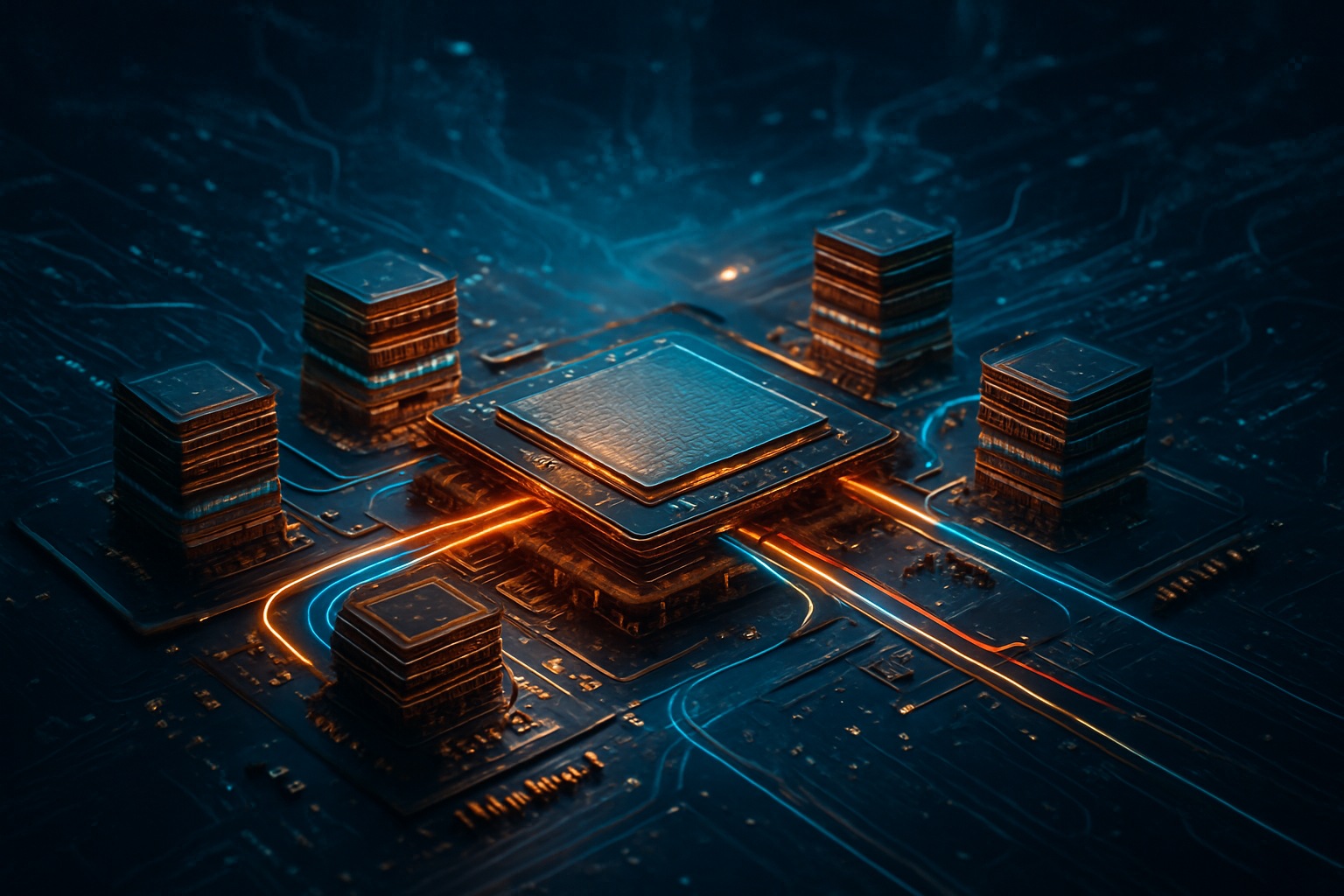
At the heart of this manufacturing crisis is the sheer physical complexity of modern AI hardware. As of January 2026, NVIDIA’s newly unveiled Rubin R100 GPUs and its predecessor, the Blackwell B200, have pushed silicon manufacturing to its theoretical limits. Because these chips are now larger than a single "reticle" (the maximum size a lithography machine can print in one pass), TSMC must use CoWoS-L technology to stitch together multiple chiplets using silicon bridges. This process allows for a massive "Super-Chip" architecture that behaves as a single unit but requires microscopic precision to assemble, leading to lower yields and longer production cycles than traditional monolithic chips.
The integration of sixth-generation High Bandwidth Memory (HBM4) has further complicated the technical landscape. Rubin chips require the integration of up to 12 stacks of HBM4, which utilize a 2048-bit interface—double the width of previous generations. This requires a staggering density of vertical and horizontal interconnects that are highly sensitive to thermal warpage during the bonding process. To combat this, TSMC has transitioned to "Hybrid Bonding" techniques, which eliminate traditional solder bumps in favor of direct copper-to-copper connections. While this increases performance and reduces heat, it demands a "clean room" environment that rivals the purity of front-end wafer fabrication, essentially turning "packaging"—historically a low-tech backend process—into a high-stakes extension of the foundry itself.
Industry experts and researchers at the International Solid-State Circuits Conference (ISSCC) have noted that this shift represents the most significant change in semiconductor manufacturing in two decades. Previously, the industry relied on "Moore's Law" through transistor scaling; today, we have entered the era of "System-on-Integrated-Chips" (SoIC). The consensus among the research community is that the packaging is no longer just a protective shell but an integral part of the compute engine. If the interposer or the bridge fails, the entire $40,000 GPU becomes a multi-thousand-dollar paperweight, making yield management the most guarded secret in the industry.
The Corporate Arms Race: Anchor Tenants and Emerging Rivals
The strategic implications of this capacity shortage are reshaping the hierarchy of Big Tech. NVIDIA remains the "anchor tenant" of TSMC’s advanced packaging ecosystem, reportedly securing nearly 60% of total CoWoS output for 2026 to support its shift to a relentless 12-month release cycle. This dominant position has forced competitors like AMD and Broadcom (NASDAQ: AVGO)—which produces custom AI TPUs for Google and Meta—to fight over the remaining 40%. The result is a tiered market where the largest players can maintain a predictable roadmap, while smaller AI startups and "Sovereign AI" initiatives by national governments face lead times exceeding nine months for high-end hardware.
In response to the TSMC bottleneck, a secondary market for advanced packaging is rapidly maturing. Intel Corporation (NASDAQ: INTC) has successfully positioned its "Foveros" and EMIB packaging technologies as a viable alternative for companies looking to de-risk their supply chains. In early 2026, Microsoft and Amazon have reportedly diverted some of their custom silicon orders to Intel's US-based packaging facilities in New Mexico and Arizona, drawn by the promise of "Sovereign AI" manufacturing. Meanwhile, Samsung Electronics (KRX: 005930) is aggressively marketing its "turnkey" solution, offering to provide both the HBM4 memory and the I-Cube packaging in a single contract—a move designed to undercut TSMC’s fragmented supply chain where memory and packaging are often handled by different entities.
The strategic advantage for 2026 belongs to those who have vertically integrated or secured long-term capacity agreements. Companies like Amkor Technology (NASDAQ: AMKR) have seen their stock soar as they take on "overflow" 2.5D packaging tasks that TSMC no longer has the bandwidth to handle. However, the reliance on Taiwan remains the industry's greatest vulnerability. While TSMC is expanding into Arizona and Japan, those facilities are still primarily focused on wafer fabrication; the most advanced CoWoS-L and SoIC assembly remains concentrated in Taiwan's AP6 and AP7 fabs, leaving the global AI economy tethered to the geopolitical stability of the Taiwan Strait.
A Choke Point Within a Choke Point: The Broader AI Landscape
The 2026 CoWoS crisis is a symptom of a broader trend: the "physicalization" of the AI boom. For years, the narrative around AI focused on software, neural network architectures, and data. Today, the limiting factor is the physical reality of atoms, heat, and microscopic wires. This packaging bottleneck has effectively created a "hard ceiling" on the growth of the global AI compute capacity. Even if the world could build a dozen more "Giga-fabs" to print silicon wafers, they would still sit idle without the specialized "pick-and-place" and bonding equipment required to finish the chips.
This development has profound impacts on the AI landscape, particularly regarding the cost of entry. The capital expenditure required to secure a spot in the CoWoS queue is so high that it is accelerating the consolidation of AI power into the hands of a few trillion-dollar entities. This "packaging tax" is being passed down to consumers and enterprise clients, keeping the cost of training Large Language Models (LLMs) high and potentially slowing the democratization of AI. Furthermore, it has spurred a new wave of innovation in "packaging-efficient" AI, where researchers are looking for ways to achieve high performance using smaller, more easily packaged chips rather than the massive "Super-Chips" that currently dominate the market.
Comparatively, the 2026 packaging crisis mirrors the oil shocks of the 1970s—a realization that a vital global resource is controlled by a tiny number of suppliers and subject to extreme physical constraints. This has led to a surge in government subsidies for "Backend" manufacturing, with the US CHIPS Act and similar European initiatives finally prioritizing packaging plants as much as wafer fabs. The realization has set in: a chip is not a chip until it is packaged, and without that final step, the "Silicon Intelligence" remains trapped in the wafer.
Looking Ahead: Panel-Level Packaging and the 2027 Roadmap
The near-term solution to the 2026 bottleneck involves the massive expansion of TSMC’s Advanced Backend Fab 7 (AP7) in Chiayi and the repurposing of former display panel plants for "AP8." However, the long-term future of the industry lies in a transition from Wafer-Level Packaging to Fan-Out Panel-Level Packaging (FOPLP). By using large rectangular panels instead of circular 300mm wafers, manufacturers can increase the number of chips processed in a single batch by up to 300%. TSMC and its partners are already conducting pilot runs for FOPLP, with expectations that it will become the high-volume standard by late 2027 or 2028.
Another major hurdle on the horizon is the transition to "Glass Substrates." As the number of chiplets on a single package increases, the organic substrates currently in use are reaching their limits of structural integrity and electrical performance. Intel has taken an early lead in glass substrate research, which could allow for even denser interconnects and better thermal management. If successful, this could be the catalyst that allows Intel to break TSMC's packaging monopoly in the latter half of the decade. Experts predict that the winner of the "Glass Race" will likely dominate the 2028-2030 AI hardware cycle.
Conclusion: The Final Frontier of Moore's Law
The current state of advanced packaging represents a fundamental shift in the history of computing. As of January 2026, the industry has accepted that the future of AI does not live on a single piece of silicon, but in the sophisticated "cities" of chiplets built through CoWoS and its successors. TSMC’s ability to scale this technology has made it the most indispensable company in the world, yet the extreme concentration of this capability has created a fragile equilibrium for the global economy.
For the coming months, the industry will be watching two key indicators: the yield rates of HBM4 integration and the speed at which TSMC can bring its AP7 Phase 2 capacity online. Any delay in these areas will have a cascading effect, delaying the release of next-generation AI models and cooling the current investment cycle. In the 2020s, we learned that data is the new oil; in 2026, we are learning that advanced packaging is the refinery. Without it, the "crude" silicon of the AI revolution remains useless.
This content is intended for informational purposes only and represents analysis of current AI developments.
TokenRing AI delivers enterprise-grade solutions for multi-agent AI workflow orchestration, AI-powered development tools, and seamless remote collaboration platforms.
For more information, visit https://www.tokenring.ai/.