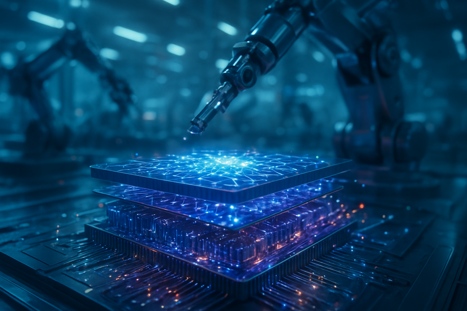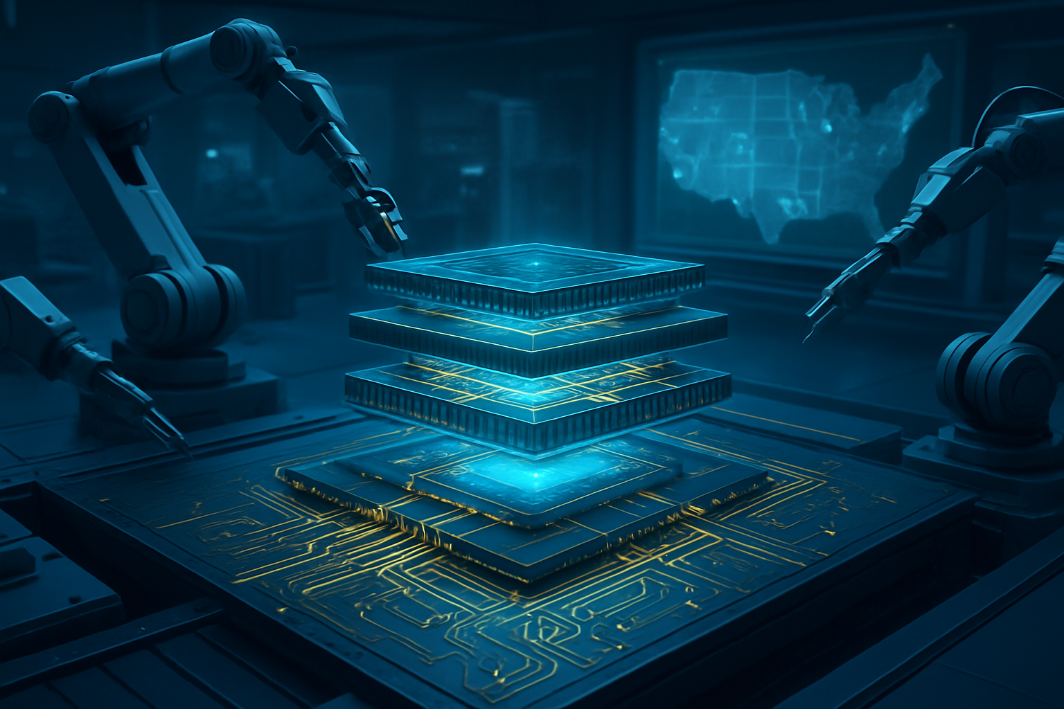
As of January 7, 2026, the global semiconductor industry has reached a critical inflection point. For decades, organic materials like Ajinomoto Build-up Film (ABF) served as the foundation for chip packaging, but the insatiable power and size requirements of modern Artificial Intelligence (AI) have finally pushed these materials to their physical limits. In a move that analysts are calling a "once-in-a-generation" shift, industry titans are transitioning to glass substrates—a breakthrough that promises to unlock a new level of performance for the massive, multi-die packages required for next-generation AI accelerators.
The immediate significance of this development cannot be overstated. With AI chips now exceeding 1,000 watts of thermal design power (TDP) and reaching physical dimensions that would cause traditional organic substrates to warp or crack, glass provides the structural integrity and electrical precision necessary to keep Moore’s Law alive. This transition is not merely an incremental upgrade; it is a fundamental re-engineering of how the world's most powerful chips are built, enabling a 10x increase in interconnect density and a 40% reduction in signal loss.
The Technical Leap: From Organic Polymers to Precision Glass
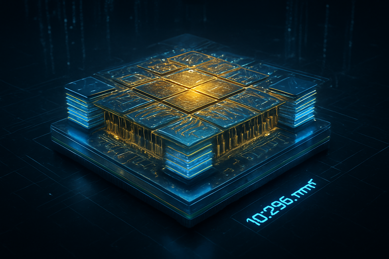
The shift to glass substrates is driven by the failure of organic materials to scale alongside the "chiplet" revolution. Traditional organic substrates are prone to "warpage"—the physical deforming of the material under high temperatures—which limits the size of a chip package to roughly 55mm x 55mm. As AI GPUs from companies like NVIDIA (NASDAQ: NVDA) and AMD (NASDAQ: AMD) grow to 100mm x 100mm and beyond, the industry has hit what experts call the "warpage wall." Glass, with its superior thermal stability, remains flat even at temperatures exceeding 500°C, matching the coefficient of thermal expansion of silicon and preventing the catastrophic mechanical failures seen in organic designs.
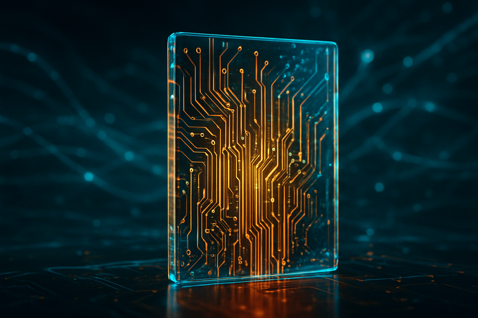
Technically, the most significant advancement lies in Through-Glass Vias (TGVs). Unlike the mechanical drilling used for organic substrates, TGVs are etched using high-precision lasers, allowing for an interconnect pitch of less than 10 micrometers—a 10x improvement over the 100-micrometer pitch common in organic materials. This density allows for significantly more "tiles" or chiplets to be packed into a single package, facilitating the massive memory bandwidth required for Large Language Models (LLMs). Furthermore, glass's ultra-low dielectric loss improves signal integrity by nearly 40%, which translates to a power consumption reduction of up to 50% for data movement within the chip.
Initial reactions from the AI research community and industry experts have been overwhelmingly positive. At the recent CES 2026 "First Look" event, analysts noted that glass substrates are the "critical enabler" for 2.5D and 3D packaging. While organic substrates still dominate mainstream consumer electronics, the high-performance computing (HPC) sector has reached a consensus: without glass, the physical size of AI clusters would be capped by the mechanical limits of plastic, effectively stalling AI hardware progress.
Competitive Landscapes: Intel, Samsung, and the Race for Packaging Dominance
The transition to glass has sparked a fierce competition among the world’s leading foundries and IDMs. Intel Corporation (NASDAQ: INTC) has emerged as an early technical pioneer, having officially reached High-Volume Manufacturing (HVM) for its 18A node as of early 2026. Intel’s dedicated glass substrate facility in Chandler, Arizona, has successfully transitioned from pilot phases to supporting commercial-grade packaging. By offering glass-based solutions to its foundry customers, Intel is positioning itself as a formidable alternative to TSMC (NYSE: TSM), specifically targeting NVIDIA and AMD's high-end business.
Samsung (KRX: 005930) is not far behind. Samsung Electro-Mechanics (SEMCO) has fast-tracked its "dream substrate" program, completing verification of its high-volume pilot line in Sejong, South Korea, in late 2025. Samsung announced at CES 2026 that it is on track for full-scale mass production by the end of the year. To bolster its competitive edge, Samsung has formed a "triple alliance" between its substrate, electronics, and display divisions, leveraging its expertise in glass processing from the smartphone and TV industries.
Meanwhile, TSMC has been forced to pivot. Originally focused on silicon interposers (CoWoS), the Taiwanese giant revived its glass substrate R&D in late 2024 under intense pressure from its primary customer, NVIDIA. As of January 2026, TSMC is aggressively pursuing Fan-Out Panel-Level Packaging (FO-PLP) on glass. This "Rectangular Revolution" involves moving from 300mm circular silicon wafers to large 600mm x 600mm rectangular glass panels. This shift increases area utilization from 57% to over 80%, drastically reducing the "AI chip bottleneck" by allowing more chips to be packaged simultaneously and at a lower cost per unit.
Wider Significance: Moore’s Law and the Energy Efficiency Frontier
The adoption of glass substrates fits into a broader trend known as "More than Moore," where performance gains are achieved through advanced packaging rather than just transistor shrinking. As it becomes increasingly difficult and expensive to shrink transistors below the 2nm threshold, the ability to package multiple specialized chiplets together with high-speed, low-power interconnects becomes the primary driver of computing power. Glass is the medium that makes this "Lego-style" chip building possible at the scale required for future AI.
Beyond raw performance, the move to glass has profound implications for energy efficiency. Data centers currently consume a significant portion of global electricity, with a large percentage of that energy spent moving data between processors and memory. By reducing signal attenuation and cutting power consumption by up to 50%, glass substrates offer a rare opportunity to improve the sustainability of AI infrastructure. This is particularly relevant as global regulators begin to scrutinize the carbon footprint of massive AI training clusters.
However, the transition is not without concerns. Glass is inherently brittle, and manufacturers are currently grappling with breakage rates that are 5-10% higher than organic alternatives. This has necessitated entirely new automated handling systems and equipment from vendors like Applied Materials (NASDAQ: AMAT) and Coherent (NYSE: COHR). Furthermore, initial mass production yields are hovering between 70% and 75%, trailing the 90%+ maturity of organic substrates, leading to a temporary cost premium for the first generation of glass-packaged chips.
Future Horizons: Optical I/O and the 2030 Roadmap
Looking ahead, the near-term focus will be on stabilizing yields and standardizing panel sizes to bring down costs. Experts predict that while glass substrates currently carry a 3x to 5x cost premium, aggressive cost reduction roadmaps will see prices decline by 40-60% by 2030 as manufacturing scales. The first commercial products to feature full glass core integration are expected to hit the market in late 2026 and early 2027, likely appearing in NVIDIA’s "Rubin" architecture and AMD’s MI400 series accelerators.
The long-term potential of glass extends into the realm of Silicon Photonics. Because glass is transparent and thermally stable, it is being positioned as the primary medium for Co-Packaged Optics (CPO). In this future scenario, data will be moved via light rather than electricity, virtually eliminating latency and power loss in AI clusters. Companies like Amazon (NASDAQ: AMZN) and SKC (KRX: 011790)—through its subsidiary Absolics—are already exploring how glass can facilitate this transition to optical computing.
The primary challenge remains the "fragility gap." As chips become larger and more complex, the risk of a microscopic crack ruining a multi-thousand-dollar processor is a major hurdle. Experts predict that the next two years will see a surge in innovation regarding "tempered" glass substrates and specialized protective coatings to mitigate these risks.
A Paradigm Shift in Semiconductor History
The transition to glass substrates represents one of the most significant material changes in semiconductor history. It marks the end of the organic era for high-performance computing and the beginning of a new age where the package is as critical as the silicon it holds. By breaking the "warpage wall," Intel, Samsung, and TSMC are ensuring that the hardware requirements of artificial intelligence do not outpace the physical capabilities of our materials.
Key takeaways from this shift include the 10x increase in interconnect density, the move toward rectangular panel-level packaging, and the critical role of glass in enabling future optical interconnects. While the transition is currently expensive and technically challenging, the performance benefits are too great to ignore. In the coming weeks and months, the industry will be watching for the first yield reports from Absolics’ Georgia facility and further details on NVIDIA’s integration of glass into its 2027 roadmap. The "Glass Age" of semiconductors has officially arrived.
This content is intended for informational purposes only and represents analysis of current AI developments.
TokenRing AI delivers enterprise-grade solutions for multi-agent AI workflow orchestration, AI-powered development tools, and seamless remote collaboration platforms.
For more information, visit https://www.tokenring.ai/.