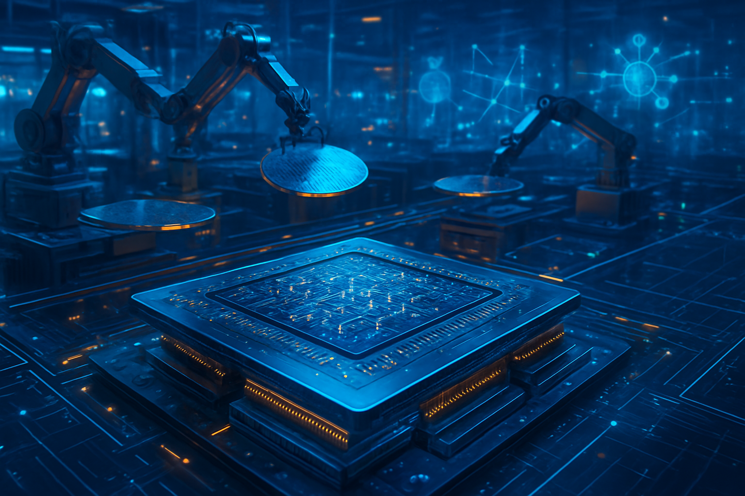
As 2025 draws to a close, the primary bottleneck in the global artificial intelligence race has shifted from the raw fabrication of silicon wafers to the intricate art of advanced packaging. Taiwan Semiconductor Manufacturing Company (TSMC) (NYSE: TSM) has officially set its sights on a massive expansion for 2026, aiming to increase its CoWoS (Chip-on-Wafer-on-Substrate) capacity by at least 33%. This aggressive roadmap is a direct response to the insatiable demand for next-generation AI accelerators, particularly as Nvidia (NASDAQ: NVDA) prepares to transition from its Blackwell Ultra series to the revolutionary Rubin architecture.
This capacity surge represents a pivotal moment in the semiconductor industry. For the past two years, the "packaging gap" has been the single greatest constraint on the deployment of large-scale AI clusters. By targeting a monthly output of 120,000 to 130,000 wafers by the end of 2026—up from approximately 90,000 at the close of 2025—TSMC is signaling that the era of "System-on-Package" is no longer a niche specialty, but the new standard for high-performance computing.
The Technical Evolution: From CoWoS-L to SoIC Integration
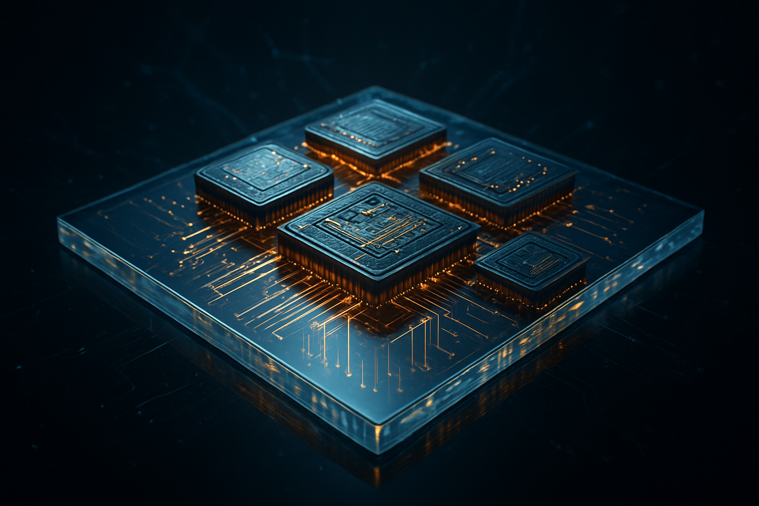
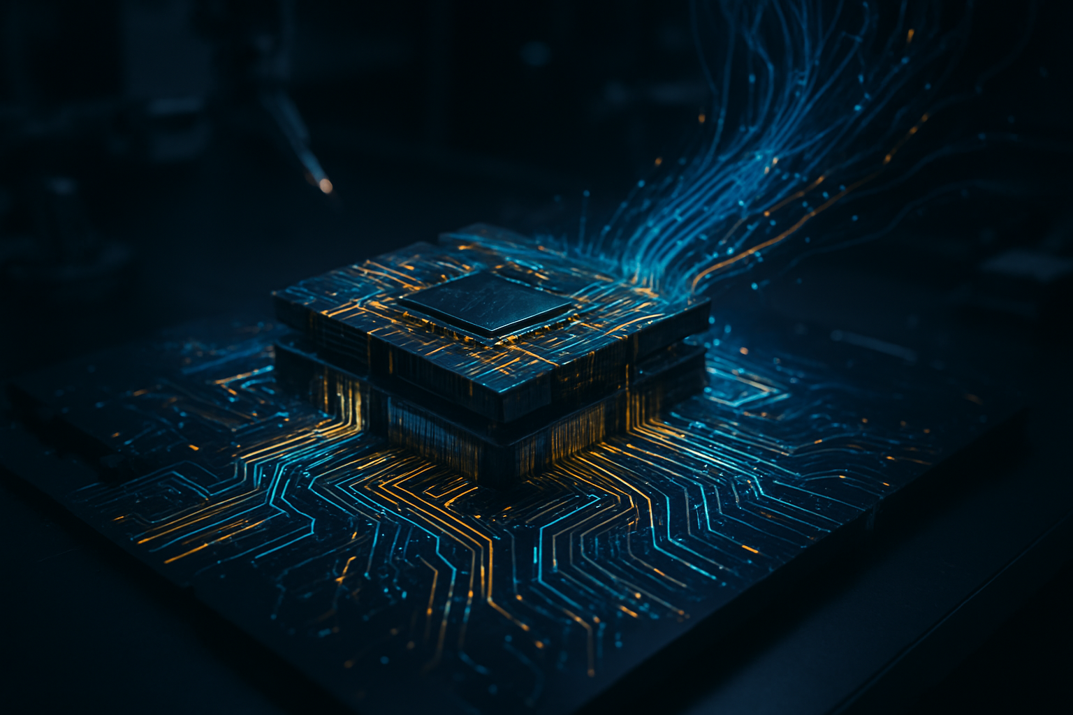
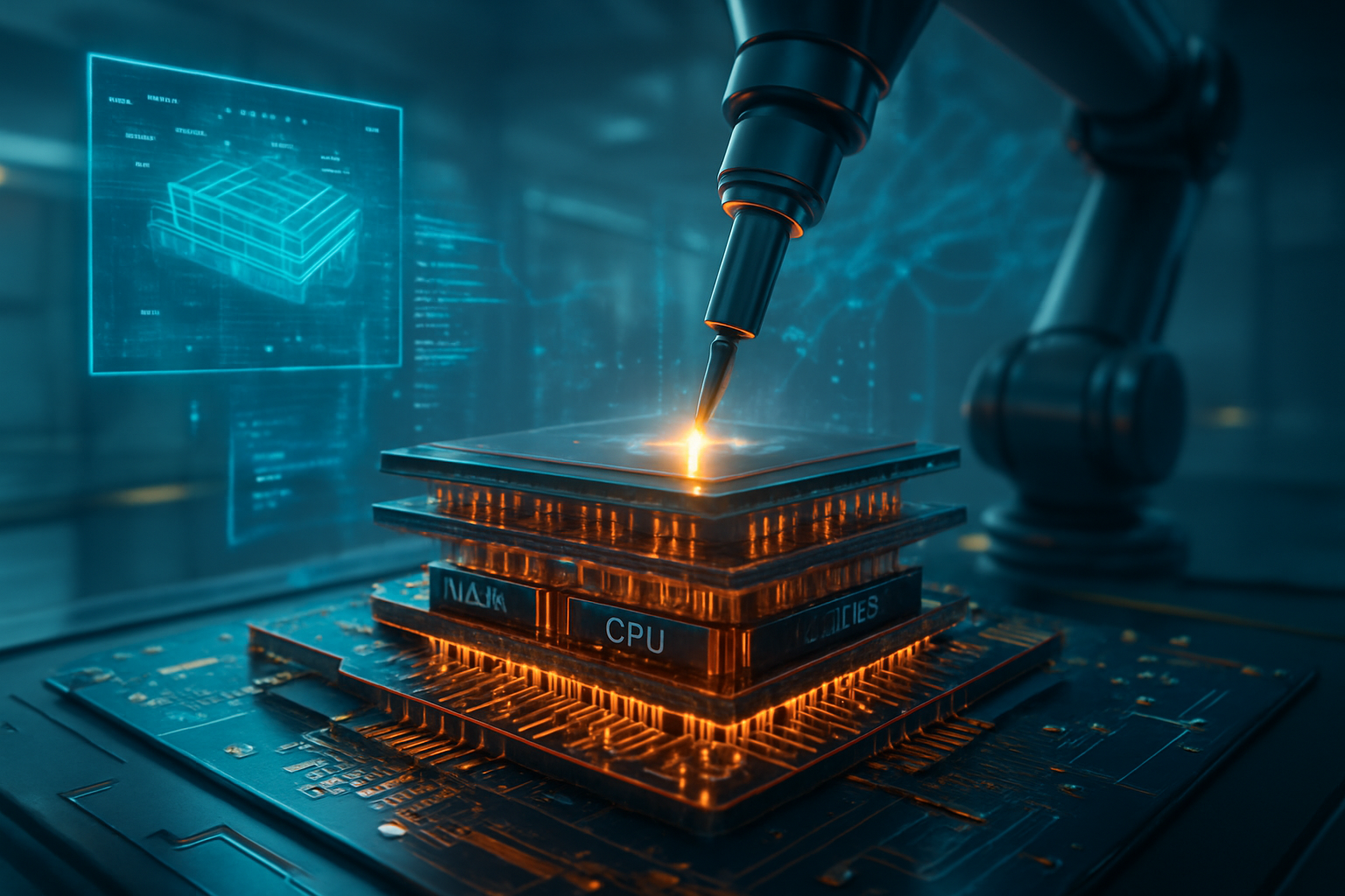
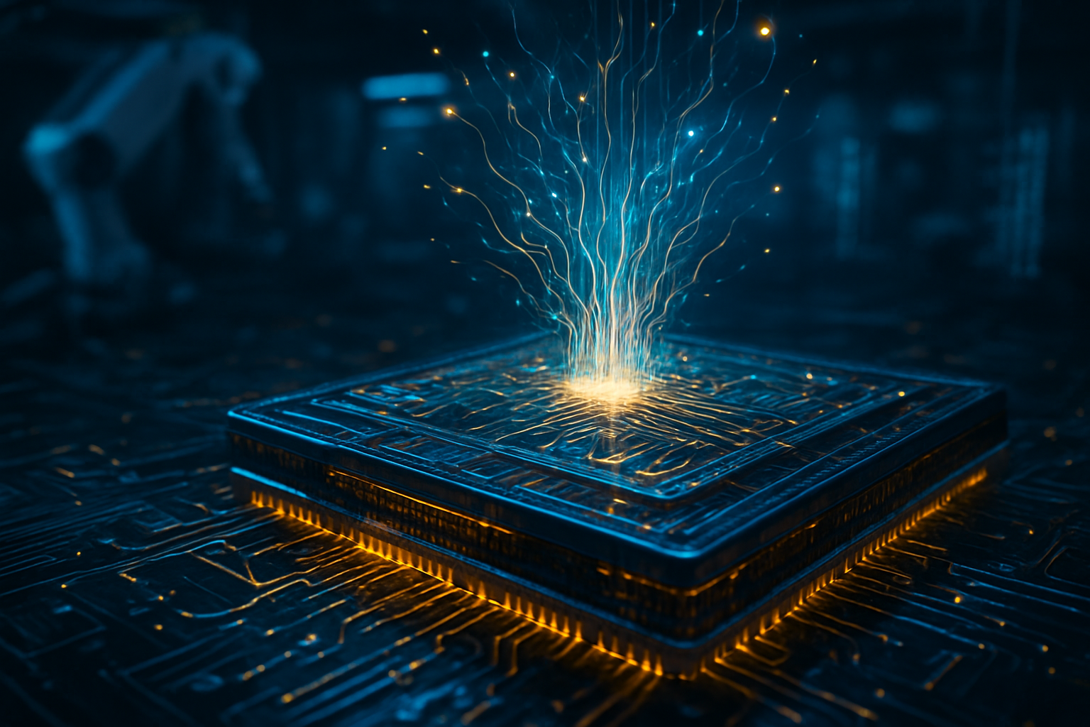
The technical complexity of AI chips has scaled faster than traditional manufacturing methods can keep pace with. TSMC’s expansion is not merely about building more of the same; it involves a sophisticated transition to CoWoS-L (Local Silicon Interconnect) and SoIC (System on Integrated Chips) technologies. While earlier iterations of CoWoS used a silicon interposer (CoWoS-S), the new CoWoS-L utilizes local silicon bridges to connect logic and memory dies. This shift is essential for Nvidia’s Blackwell Ultra, which features a 3.3x reticle size interposer and 288GB of HBM3e memory. The "L" variant allows for larger package sizes and better thermal management, addressing the warping and CTE (Coefficient of Thermal Expansion) mismatch issues that plagued early high-power designs.
Looking toward 2026, the focus shifts to the Rubin (R100) architecture, which will be the first major GPU to heavily leverage SoIC technology. SoIC enables true 3D vertical stacking, allowing logic-on-logic or logic-on-memory bonding with significantly reduced bump pitches of 9 to 10 microns. This transition is critical for the integration of HBM4, which requires the extreme precision of SoIC due to its 2,048-bit interface. Industry experts note that the move to a 4.0x reticle size for Rubin pushes the physical limits of organic substrates, necessitating the massive investments TSMC is making in its AP7 and AP8 facilities in Chiayi and Tainan.
A High-Stakes Land Grab: Nvidia, AMD, and the Capacity Squeeze
The market implications of TSMC’s expansion are profound. Nvidia (NASDAQ: NVDA) has reportedly pre-booked over 50% of TSMC’s total 2026 advanced packaging output, securing a dominant position that leaves its rivals scrambling. This "capacity lock" provides Nvidia with a significant strategic advantage, ensuring that it can meet the volume requirements for Blackwell Ultra in early 2026 and the Rubin ramp-up later that year. For competitors like Advanced Micro Devices (NASDAQ: AMD) and major Cloud Service Providers (CSPs) developing their own silicon, the remaining capacity is a precious and dwindling resource.
AMD (NASDAQ: AMD) is increasingly turning to SoIC for its MI350 series to stay competitive in interconnect density, while companies like Broadcom (NASDAQ: AVGO) and Marvell (NASDAQ: MRVL) are fighting for CoWoS slots to support custom AI ASICs for Google and Amazon. This squeeze has forced many firms to diversify their supply chains, looking toward Outsourced Semiconductor Assembly and Test (OSAT) providers like Amkor Technology (NASDAQ: AMKR) and ASE Technology (NYSE: ASX). However, for the most advanced 3D-stacked designs, TSMC remains the only "one-stop shop" capable of delivering the required yields at scale, further solidifying its role as the gatekeeper of the AI era.
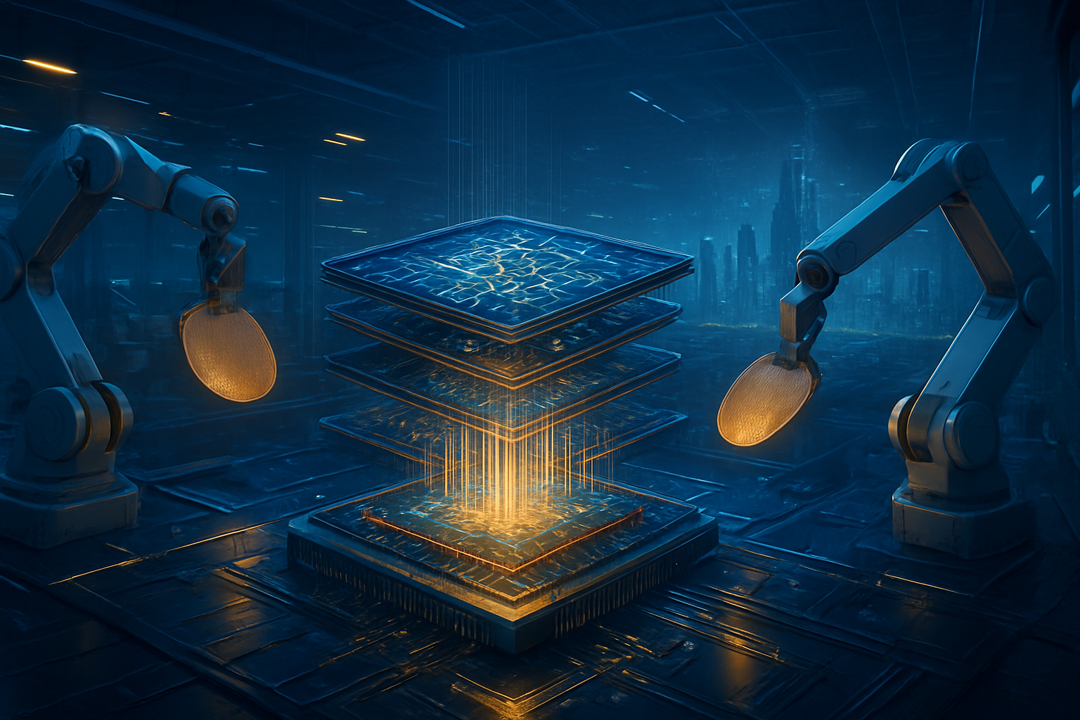
Redefining Moore’s Law through Heterogeneous Integration
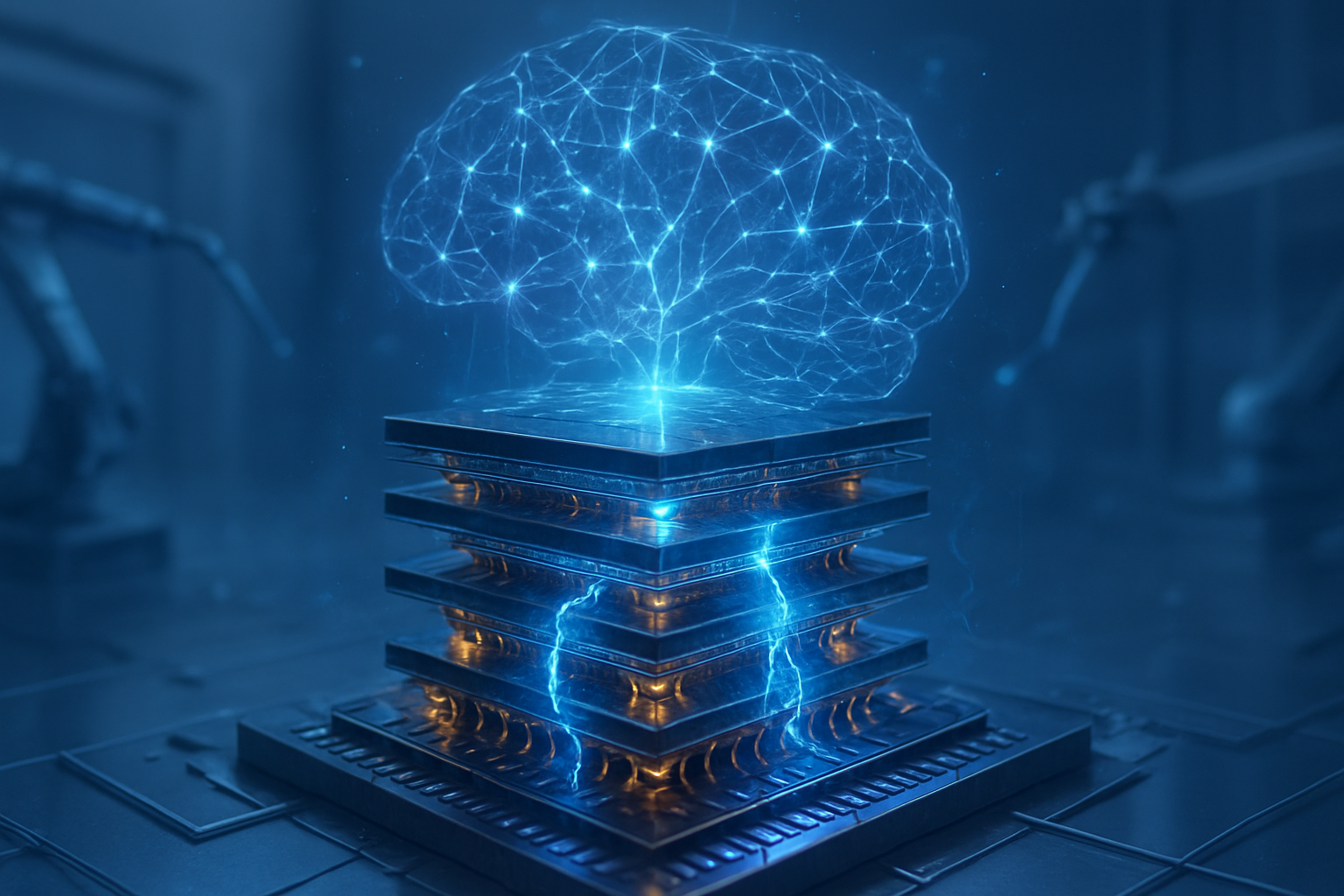
The wider significance of this expansion lies in the fundamental transformation of semiconductor manufacturing. As traditional 2D scaling (shrinking transistors) reaches its physical and economic limits, the industry has pivoted toward "More than Moore" strategies. Advanced packaging is the vehicle for this change, allowing different chiplets—optimized for memory, logic, or I/O—to be fused into a single, high-performance unit. This shift effectively moves the frontier of innovation from the foundry to the packaging facility.
However, this transition is not without its risks. The extreme concentration of advanced packaging capacity in Taiwan remains a point of geopolitical concern. While TSMC has announced plans for advanced packaging in Arizona, meaningful volume is not expected until 2027 or 2028. Furthermore, the reliance on specialized equipment from vendors like Advantest (OTC: ADTTF) and Besi (AMS: BESI) creates a secondary layer of bottlenecks. If equipment lead times—currently sitting at 6 to 9 months—do not improve, even TSMC’s aggressive facility expansion may face delays, potentially slowing the global pace of AI development.
The Horizon: Glass Substrates and the Path to 2027
Looking beyond 2026, the industry is already preparing for the next major leap: the transition to glass substrates. As package sizes exceed 100x100mm, organic substrates begin to lose structural integrity and electrical performance. Glass offers superior flatness and thermal stability, which will be necessary for the post-Rubin era of AI chips. Intel (NASDAQ: INTC) has been a vocal proponent of glass substrates, and TSMC is expected to integrate this technology into its 3DFabric roadmap by 2027 to support even larger multi-die configurations.
Furthermore, the industry is closely watching the development of Panel-Level Packaging (PLP), which could offer a more cost-effective way to scale capacity by using large rectangular panels instead of circular wafers. While still in its infancy for high-end AI applications, PLP represents the next logical step in driving down the cost of advanced packaging, potentially democratizing access to high-performance compute for smaller AI labs and startups that are currently priced out of the market.
Conclusion: A New Era of Compute
TSMC’s commitment to a 33% capacity increase by 2026 marks the end of the "experimental" phase of advanced packaging and the beginning of its industrialization at scale. The transition to CoWoS-L and SoIC is not just a technical upgrade; it is a total reconfiguration of how AI hardware is built, moving from monolithic chips to complex, three-dimensional systems. This expansion is the foundation upon which the next generation of LLMs and autonomous agents will be built.
As we move into 2026, the industry will be watching two key metrics: the yield rates of the massive 4.0x reticle Rubin chips and the speed at which TSMC can bring its new AP7 and AP8 facilities online. If TSMC succeeds in breaking the packaging bottleneck, it will pave the way for a decade of unprecedented growth in AI capabilities. However, if supply continues to lag behind the exponential demand of the AI giants, the industry may find that the limits of artificial intelligence are defined not by code, but by the physical constraints of silicon and solder.
This content is intended for informational purposes only and represents analysis of current AI developments.
TokenRing AI delivers enterprise-grade solutions for multi-agent AI workflow orchestration, AI-powered development tools, and seamless remote collaboration platforms.
For more information, visit https://www.tokenring.ai/.