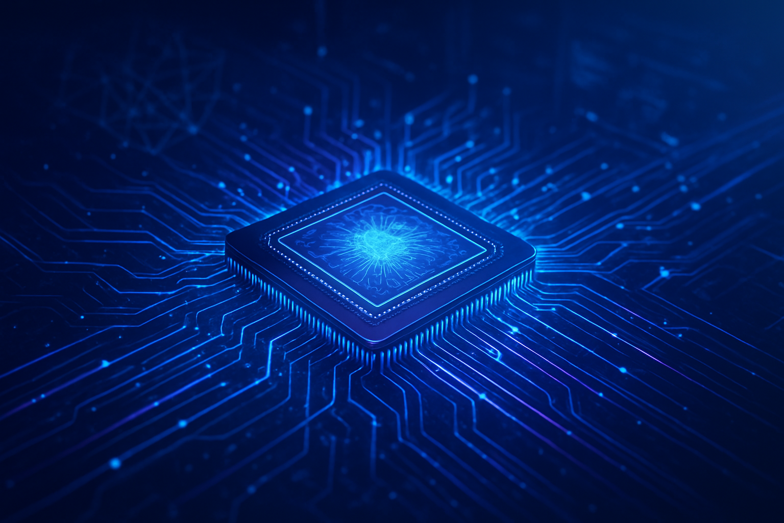
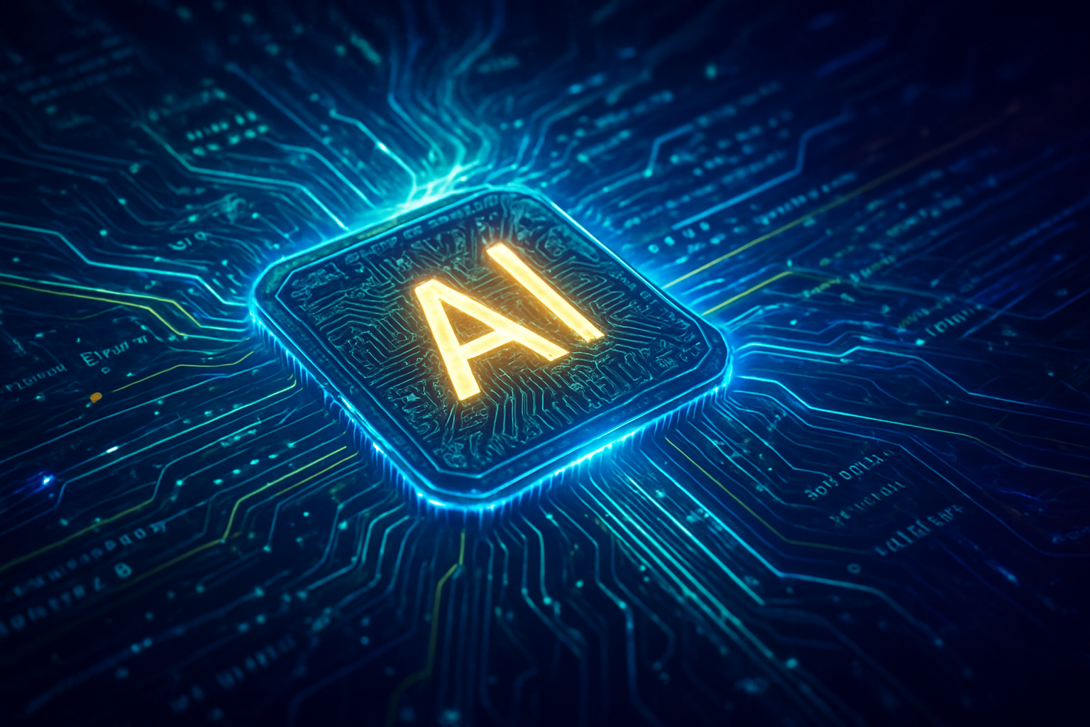
Tag: Advanced Packaging

  • The Silicon Revolution: How Next-Gen Semiconductor Innovations are Forging the Future of AI

    The Silicon Revolution: How Next-Gen Semiconductor Innovations are Forging the Future of AI

    The landscape of artificial intelligence is undergoing a profound transformation, driven by an unprecedented surge in semiconductor innovation. Far from incremental improvements, the industry is witnessing a Cambrian explosion of breakthroughs in chip design, manufacturing, and materials science, directly enabling the development of more powerful, efficient, and versatile AI systems. These advancements are not merely enhancing existing AI capabilities but are fundamentally reshaping the trajectory of artificial intelligence, promising a future where AI is more intelligent, ubiquitous, and sustainable.

    At the heart of this revolution are innovations that dramatically improve performance, energy efficiency, and miniaturization, while simultaneously accelerating the development cycles for AI hardware. From vertically stacked chiplets to atomic-scale lithography and brain-inspired computing architectures, these technological leaps are addressing the insatiable computational demands of modern AI, particularly the training and inference of increasingly complex models like large language models (LLMs). The immediate significance is a rapid expansion of what AI can achieve, pushing the boundaries of machine learning and intelligent automation across every sector.

    Unpacking the Technical Marvels Driving AI's Evolution

    The current wave of AI semiconductor innovation is characterized by several key technical advancements, each contributing significantly to the enhanced capabilities of AI hardware. These breakthroughs represent a departure from traditional planar scaling, embracing new dimensions and materials to overcome physical limitations.

    One of the most impactful areas is advanced packaging technologies, which are crucial as conventional two-dimensional scaling approaches reach their limits. Techniques like 2.5D and 3D stacking, along with heterogeneous integration, involve vertically stacking multiple chips or "chiplets" within a single package. This dramatically increases component density and shortens interconnect paths, leading to substantial performance gains (up to 50% improvement in performance per watt for AI accelerators) and reduced latency. Companies like Taiwan Semiconductor Manufacturing Company (TSMC: TPE), Samsung Electronics (SSNLF: KRX), Advanced Micro Devices (AMD: NASDAQ), and Intel Corporation (INTC: NASDAQ) are at the forefront, utilizing platforms such as CoWoS, SoIC, SAINT, and Foveros. High Bandwidth Memory (HBM), often vertically stacked and integrated close to the GPU, is another critical component, addressing the "memory wall" by providing the massive data transfer speeds and lower power consumption essential for training large AI models.

    Advanced lithography continues to push the boundaries of miniaturization. The emergence of High Numerical Aperture (High-NA) Extreme Ultraviolet (EUV) lithography is a game-changer, offering higher resolution (8 nm compared to current EUV's 0.33 NA). This enables transistors that are 1.7 times smaller and nearly triples transistor density, paving the way for advanced nodes like 2nm and below. These smaller, more energy-efficient transistors are vital for developing next-generation AI chips. Furthermore, Multicolumn Electron Beam Lithography (MEBL) increases interconnect pitch density, significantly reducing data path length and energy consumption for chip-to-chip communication, a critical factor for high-performance computing (HPC) and AI applications.

    Beyond silicon, research into new materials and architectures is accelerating. Neuromorphic computing, inspired by the human brain, utilizes spiking neural networks (SNNs) for highly energy-efficient processing. Intel's Loihi and IBM's TrueNorth and NorthPole are pioneering examples, promising dramatic reductions in power consumption for AI, making it more sustainable for edge devices. Additionally, 2D materials like graphene and carbon nanotubes (CNTs) offer superior flexibility, conductivity, and energy efficiency, potentially surpassing silicon. CNT-based Tensor Processing Units (TPUs), for instance, have shown efficiency improvements of up to 1,700 times compared to silicon TPUs for certain tasks, opening doors for highly compact and efficient monolithic 3D integrations. Initial reactions from the AI research community and industry experts highlight the revolutionary potential of these advancements, noting their capability to fundamentally alter the performance and power consumption profiles of AI hardware.

    Corporate Impact and Competitive Realignments

    These semiconductor innovations are creating significant ripples across the AI industry, benefiting established tech giants and fueling the growth of innovative startups, while also disrupting existing market dynamics.

    Companies like TSMC and Samsung Electronics (SSNLF: KRX) are poised to be major beneficiaries, as their leadership in advanced packaging and lithography positions them as indispensable partners for virtually every AI chip designer. Their cutting-edge fabrication capabilities are the bedrock upon which next-generation AI accelerators are built. NVIDIA Corporation (NVDA: NASDAQ), a dominant force in AI GPUs, continues to leverage these advancements in its architectures like Blackwell and Rubin, maintaining its competitive edge by delivering increasingly powerful and efficient AI compute platforms. Intel Corporation (INTC: NASDAQ), through its Foveros packaging and investments in neuromorphic computing (Loihi), is aggressively working to regain market share in the AI accelerator space. Similarly, Advanced Micro Devices (AMD: NASDAQ) is making significant strides with its 3D V-Cache technology and MI series accelerators, challenging NVIDIA's dominance.

    The competitive implications are profound. Major AI labs and tech companies are in a race to secure access to the most advanced fabrication technologies and integrate these innovations into their custom AI chips. Google (GOOGL: NASDAQ), with its Tensor Processing Units (TPUs), continues to push the envelope in specialized AI ASICs, directly benefiting from advanced packaging and smaller process nodes. Qualcomm Technologies (QCOM: NASDAQ) is leveraging these advancements to deliver powerful and efficient AI processing capabilities for edge devices and mobile platforms, enabling a new generation of on-device AI. This intense competition is driving further innovation, as companies strive to differentiate their offerings through superior hardware performance and energy efficiency.

    Potential disruption to existing products and services is inevitable. As AI hardware becomes more powerful and energy-efficient, it enables the deployment of complex AI models in new form factors and environments, from autonomous vehicles to smart infrastructure. This could disrupt traditional cloud-centric AI paradigms by facilitating more robust edge AI, reducing latency, and enhancing data privacy. Companies that can effectively integrate these semiconductor innovations into their AI product strategies will gain significant market positioning and strategic advantages, while those that lag risk falling behind in the rapidly evolving AI landscape.

    Broader Significance and Future Horizons

    The implications of these semiconductor breakthroughs extend far beyond mere performance metrics, shaping the broader AI landscape, raising new concerns, and setting the stage for future technological milestones. These innovations are not just about making AI faster; they are about making it more accessible, sustainable, and capable of tackling increasingly complex real-world problems.

    These advancements fit into the broader AI landscape by enabling the scaling of ever-larger and more sophisticated AI models, particularly in generative AI. The ability to process vast datasets and execute intricate neural network operations with greater speed and efficiency is directly contributing to the rapid progress seen in areas like natural language processing and computer vision. Furthermore, the focus on energy efficiency, through innovations like neuromorphic computing and wide bandgap semiconductors (SiC, GaN) for power delivery, addresses growing concerns about the environmental impact of large-scale AI deployments, aligning with global sustainability trends. The pervasive application of AI within semiconductor design and manufacturing itself, via AI-powered Electronic Design Automation (EDA) tools like Synopsys' (SNPS: NASDAQ) DSO.ai, creates a virtuous cycle, accelerating the development of even better AI chips.

    Potential concerns include the escalating cost of developing and manufacturing these cutting-edge chips, which could further concentrate power among a few large semiconductor companies and nations. Supply chain vulnerabilities, as highlighted by recent global events, also remain a significant challenge. However, the benefits are substantial: these innovations are fostering the development of entirely new AI applications, from real-time personalized medicine to highly autonomous systems. 
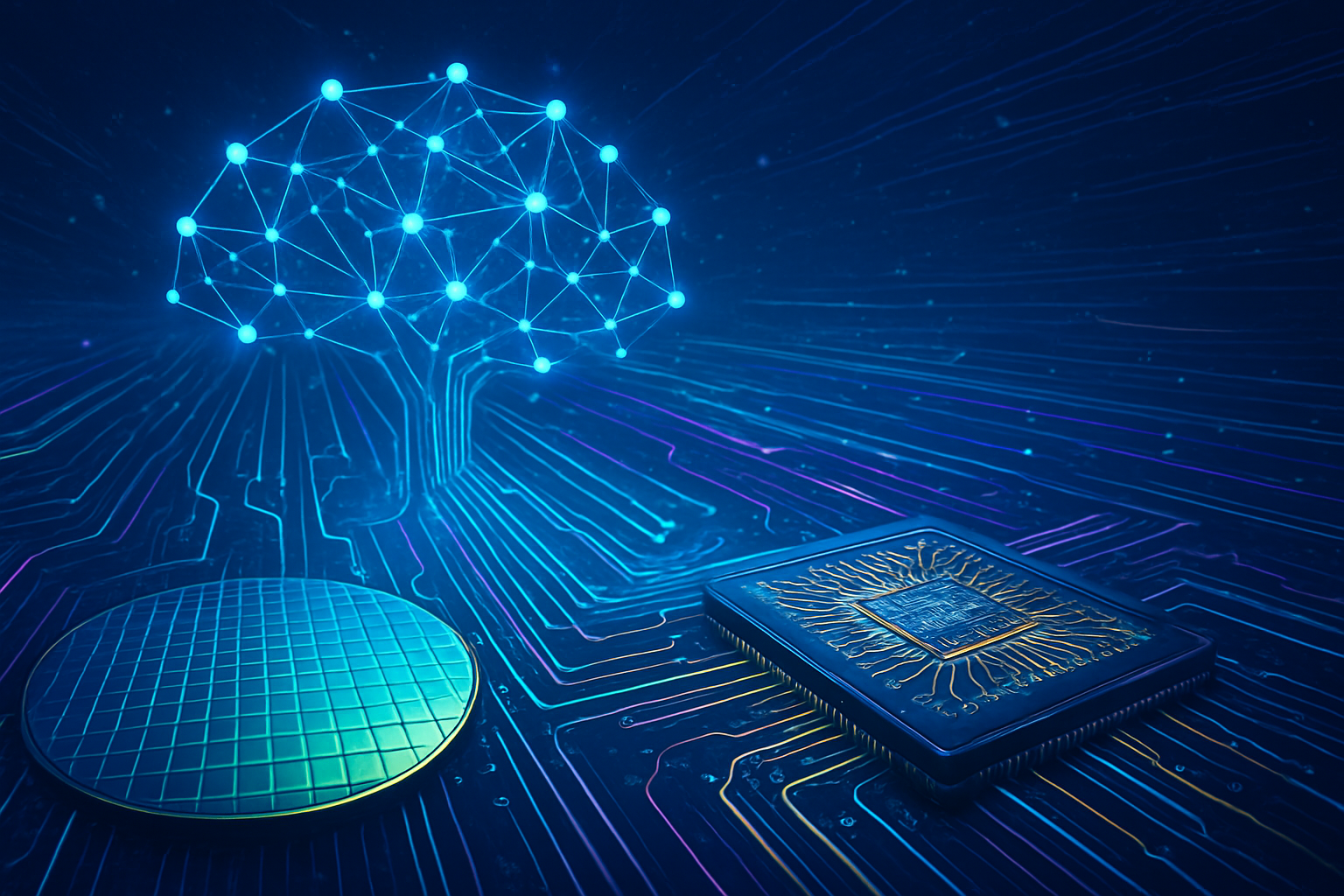
Comparing this to previous AI milestones, such as the initial breakthroughs in deep learning, the current hardware revolution represents a foundational shift that promises to accelerate the pace of AI progress exponentially, enabling capabilities that were once considered science fiction.

    Charting the Course: Expected Developments and Expert Predictions

    Looking ahead, the trajectory of AI-focused semiconductor production points towards continued rapid innovation, with significant developments expected in both the near and long term. These advancements will unlock new applications and address existing challenges, further embedding AI into the fabric of daily life and industry.

    In the near term, we can expect the widespread adoption of current advanced packaging technologies, with further refinements in 3D stacking and heterogeneous integration. The transition to smaller process nodes (e.g., 2nm and beyond) enabled by High-NA EUV will become more mainstream, leading to even more powerful and energy-efficient specialized AI chips (ASICs) and GPUs. The integration of AI into every stage of the chip lifecycle, from design to manufacturing optimization, will become standard practice, drastically reducing design cycles and improving yields. Experts predict a continued exponential growth in AI compute capabilities, driven by this hardware-software co-design paradigm, leading to more sophisticated and nuanced AI models.

    Longer term, the field of neuromorphic computing is anticipated to mature significantly, potentially leading to a new class of ultra-low-power AI processors capable of on-device learning and adaptive intelligence, profoundly impacting edge AI and IoT. Breakthroughs in novel materials like 2D materials and carbon nanotubes could lead to entirely new chip architectures that surpass the limitations of silicon, offering unprecedented performance and efficiency. Potential applications on the horizon include highly personalized and predictive AI assistants, fully autonomous robotics, and AI systems capable of scientific discovery and complex problem-solving at scales currently unimaginable. However, challenges remain, including the high cost of advanced manufacturing equipment, the complexity of integrating diverse materials, and the need for new software paradigms to fully leverage these novel hardware architectures. Experts predict that the next decade will see AI hardware become increasingly specialized and ubiquitous, moving AI from the cloud to every conceivable device and environment.

    A New Era for Artificial Intelligence: The Hardware Foundation

    The current wave of innovation in AI-focused semiconductor production marks a pivotal moment in the history of artificial intelligence. It underscores a fundamental truth: the advancement of AI is inextricably linked to the capabilities of its underlying hardware. The convergence of advanced packaging, cutting-edge lithography, novel materials, and AI-driven design automation is creating a foundational shift, enabling AI to transcend previous limitations and unlock unprecedented potential.

    The key takeaway is that these hardware breakthroughs are not just evolutionary; they are revolutionary. They are providing the necessary computational horsepower and energy efficiency to train and deploy increasingly complex AI models, from the largest generative AI systems to the smallest edge devices. This development's significance in AI history cannot be overstated; it represents a new era where hardware innovation is directly fueling the rapid acceleration of AI capabilities, making more intelligent, adaptive, and pervasive AI a tangible reality.

    In the coming weeks and months, industry observers should watch for further announcements regarding next-generation chip architectures, particularly from major players like NVIDIA (NVDA: NASDAQ), Intel (INTC: NASDAQ), and AMD (AMD: NASDAQ). Keep an eye on the progress of High-NA EUV deployment and the commercialization of novel materials and neuromorphic computing solutions. The ongoing race to deliver more powerful and efficient AI hardware will continue to drive innovation, setting the stage for the next wave of AI applications and fundamentally reshaping our technological landscape.


    This content is intended for informational purposes only and represents analysis of current AI developments.

    TokenRing AI delivers enterprise-grade solutions for multi-agent AI workflow orchestration, AI-powered development tools, and seamless remote collaboration platforms.
    For more information, visit https://www.tokenring.ai/.

  • The Indispensable Core: Why TSMC Alone Powers the Next Wave of AI Innovation

    The Indispensable Core: Why TSMC Alone Powers the Next Wave of AI Innovation

    TSMC (Taiwan Semiconductor Manufacturing Company) (NYSE: TSM) holds an utterly indispensable and pivotal role in the global AI chip supply chain, serving as the backbone for the next generation of artificial intelligence technologies. As the world's largest and most advanced semiconductor foundry, TSMC manufactures over 90% of the most cutting-edge chips, making it the primary production partner for virtually every major tech company developing AI hardware, including industry giants like Nvidia (NASDAQ: NVDA), Apple (NASDAQ: AAPL), AMD (NASDAQ: AMD), Qualcomm (NASDAQ: QCOM), Google (NASDAQ: GOOGL), Amazon (NASDAQ: AMZN), and Broadcom (NASDAQ: AVGO). Its technological leadership, characterized by advanced process nodes like 3nm and the upcoming 2nm and A14, alongside innovative 3D packaging solutions such as CoWoS (Chip-on-Wafer-on-Substrate) and SoIC (System-on-Integrated-Chips), enables the creation of AI processors that are faster, more power-efficient, and capable of integrating more computational power into smaller spaces. These capabilities are essential for training and deploying complex machine learning models, powering generative AI, large language models, autonomous vehicles, and advanced data centers, thereby directly accelerating the pace of AI innovation globally.

    The immediate significance of TSMC for next-generation AI technologies cannot be overstated; without its unparalleled manufacturing prowess, the rapid advancement and widespread deployment of AI would be severely hampered. Its pure-play foundry model fosters trust and collaboration, allowing it to work with multiple partners simultaneously without competition, further cementing its central position in the AI ecosystem. The "AI supercycle" has led to unprecedented demand for advanced semiconductors, making TSMC's manufacturing capacity and consistent high yield rates critical for meeting the industry's burgeoning needs. Any disruption to TSMC's operations could have far-reaching impacts on the digital economy, underscoring its indispensable role in enabling the AI revolution and defining the future of intelligent computing.

    Technical Prowess: The Engine Behind AI's Evolution

    TSMC has solidified its pivotal role in powering the next generation of AI chips through continuous technical advancements in both process node miniaturization and innovative 3D packaging technologies. The company's 3nm (N3) FinFET technology, introduced into high-volume production in 2022, represents a significant leap from its 5nm predecessor, offering a 70% increase in logic density, 15-20% performance gains at the same power levels, or up to 35% improved power efficiency. This allows for the creation of more complex and powerful AI accelerators without increasing chip size, a critical factor for AI workloads that demand intense computation. Building on this, TSMC's newly introduced 2nm (N2) chip, slated for mass production in the latter half of 2025, promises even more profound benefits. Utilizing first-generation nanosheet transistors and a Gate-All-Around (GAA) architecture—a departure from the FinFET design of earlier nodes—the 2nm process is expected to deliver a 10-15% speed increase at constant power or a 20-30% reduction in power consumption at the same speed, alongside a 15% boost in logic density. These advancements are crucial for enabling devices to operate faster, consume less energy, and manage increasingly intricate AI tasks more efficiently, contrasting sharply with the limitations of previous, larger process nodes.

    Complementing its advanced process nodes, TSMC has pioneered sophisticated 3D packaging technologies such as CoWoS (Chip-on-Wafer-on-Substrate) and SoIC (System-on-Integrated-Chips) to overcome traditional integration barriers and meet the demanding requirements of AI. CoWoS, a 2.5D advanced packaging solution, integrates high-performance compute dies (like GPUs) with High Bandwidth Memory (HBM) on a silicon interposer. This innovative approach drastically reduces data travel distance, significantly increases memory bandwidth, and lowers power consumption per bit transferred, which is essential for memory-bound AI workloads. Unlike traditional flip-chip packaging, which struggles with the vertical and lateral integration needed for HBM, CoWoS leverages a silicon interposer as a high-speed, low-loss bridge between dies. Further pushing the boundaries, SoIC is a true 3D chiplet stacking technology employing hybrid wafer bonding and through-silicon vias (TSV) instead of conventional metal bump stacking. This results in ultra-dense, ultra-short connections between stacked logic devices, reducing reliance on silicon interposers and yielding a smaller overall package size with high 3D interconnect density and ultra-low bonding latency for energy-efficient computing systems. SoIC-X, a bumpless bonding variant, is already being used in specific applications like AMD's (NASDAQ: AMD) MI300 series AI products, and TSMC plans for a future SoIC-P technology that can stack N2 and N3 dies. These packaging innovations are critical as they enable enhanced chip performance even as traditional transistor scaling becomes more challenging.

    The AI research community and industry experts have largely lauded TSMC's technical advancements, recognizing the company as an "undisputed titan" and "key enabler" of the AI supercycle. Analysts and experts universally acknowledge TSMC's indispensable role in accelerating AI innovation, stating that without its foundational manufacturing capabilities, the rapid evolution and deployment of current AI technologies would be impossible. Major clients such as Nvidia (NASDAQ: NVDA), AMD (NASDAQ: AMD), Apple (NASDAQ: AAPL), Google (NASDAQ: GOOGL), and OpenAI are heavily reliant on TSMC for their next-generation AI accelerators and custom AI chips, driving "insatiable demand" for the company's advanced nodes and packaging solutions. This intense demand has, however, led to concerns regarding significant bottlenecks in CoWoS advanced packaging capacity, despite TSMC's aggressive expansion plans. Furthermore, the immense R&D and capital expenditure required for these cutting-edge technologies, particularly the 2nm GAA process, are projected to result in a substantial increase in chip prices—potentially up to 50% compared to 3nm—leading to dissatisfaction among clients and raising concerns about higher costs for consumer electronics. Nevertheless, TSMC's strategic position and technical superiority are expected to continue fueling its growth, with its High-Performance Computing division (which includes AI chips) accounting for a commanding 57% of its total revenue. The company is also proactively utilizing AI to design more energy-efficient chips, aiming for a tenfold improvement, marking a "recursive innovation" where AI contributes to its own hardware optimization.

    Corporate Impact: Reshaping the AI Landscape

    TSMC (NYSE: TSM) stands as the undisputed global leader in advanced semiconductor manufacturing, making it a pivotal force in powering the next generation of AI chips. The company commands over 60% of the world's semiconductor production and more than 90% of the most advanced chips, a position reinforced by its cutting-edge process technologies like 3nm, 2nm, and the upcoming A16 nodes. These advanced nodes, coupled with sophisticated packaging solutions such as CoWoS (Chip-on-Wafer-on-Substrate), are indispensable for creating the high-performance, energy-efficient AI accelerators that drive everything from large language models to autonomous systems. The burgeoning demand for AI chips has made TSMC an indispensable "pick-and-shovel" provider, poised for explosive growth as its advanced process lines operate at full capacity, leading to significant revenue increases. This dominance allows TSMC to implement price hikes for its advanced nodes, reflecting the soaring production costs and immense demand, a structural shift that redefines the economics of the tech industry.

    TSMC's pivotal role profoundly impacts major tech giants, dictating their ability to innovate and compete in the AI landscape. Nvidia (NASDAQ: NVDA), a cornerstone client, relies solely on TSMC for the manufacturing of its market-leading AI GPUs, including the Hopper, Blackwell, and upcoming Rubin series, leveraging TSMC's advanced nodes and critical CoWoS packaging. This deep partnership is fundamental to Nvidia's AI chip roadmap and its sustained market dominance, with Nvidia even drawing inspiration from TSMC's foundry business model for its own AI foundry services. Similarly, Apple (NASDAQ: AAPL) exclusively partners with TSMC for its A-series mobile chips, M-series processors for Macs and iPads, and is collaborating on custom AI chips for data centers, securing early access to TSMC's most advanced nodes, including the upcoming 2nm process. Other beneficiaries include AMD (NASDAQ: AMD), which utilizes TSMC for its Instinct AI accelerators and other chips, and Qualcomm (NASDAQ: QCOM), which relies on TSMC for its Snapdragon SoCs that incorporate advanced on-device AI capabilities. Tech giants like Google (NASDAQ: GOOGL) and Amazon (NASDAQ: AMZN) are also deeply embedded in this ecosystem; Google is shifting its Pixel Tensor chips to TSMC's 3nm process for improved performance and efficiency, a long-term strategic move, while Amazon Web Services (AWS) is developing custom Trainium and Graviton AI chips manufactured by TSMC to reduce dependency on Nvidia and optimize costs. Even Broadcom (NASDAQ: AVGO), a significant player in custom AI and networking semiconductors, partners with TSMC for advanced fabrication, notably collaborating with OpenAI to develop proprietary AI inference chips.

    The implications of TSMC's dominance are far-reaching for competitive dynamics, product disruption, and market positioning. Companies with strong relationships and secured capacity at TSMC gain significant strategic advantages in performance, power efficiency, and faster time-to-market for their AI solutions, effectively widening the gap with competitors. Conversely, rivals like Samsung Foundry and Intel Foundry Services (NASDAQ: INTC) continue to trail TSMC significantly in advanced node technology and yield rates, facing challenges in competing directly. The rising cost of advanced chip manufacturing, driven by TSMC's price hikes, could disrupt existing product strategies by increasing hardware costs, potentially leading to higher prices for end-users or squeezing profit margins for downstream companies. For major AI labs and tech companies, the ability to design custom silicon and leverage TSMC's manufacturing expertise offers a strategic advantage, allowing them to tailor hardware precisely to their specific AI workloads, thereby optimizing performance and potentially reducing operational expenses for their services. AI startups, however, face a tougher landscape. The premium cost and stringent access to TSMC's cutting-edge nodes could raise significant barriers to entry and slow innovation for smaller entities with limited capital. Additionally, as TSMC prioritizes advanced nodes, resources may be reallocated from mature nodes, potentially leading to supply constraints and higher costs for startups that rely on these less advanced technologies. However, the trend of custom chips also presents opportunities, as seen with OpenAI's partnership with Broadcom (NASDAQ: AVGO) and TSMC (NYSE: TSM), suggesting that strategic collaborations can still enable impactful AI hardware development for well-funded AI labs.

    Wider Significance: Geopolitics, Economy, and the AI Future

    TSMC (Taiwan Semiconductor Manufacturing Company) (NYSE: TSM) plays an undeniably pivotal and indispensable role in powering the next generation of AI chips, serving as the foundational enabler for the ongoing artificial intelligence revolution. With an estimated 70.2% to 71% market share in the global pure-play wafer foundry market as of Q2 2025, and projected to exceed 90% in advanced nodes, TSMC's near-monopoly position means that virtually every major AI breakthrough, from large language models to autonomous systems, is fundamentally powered by its silicon. Its unique dedicated foundry business model, which allows fabless companies to innovate at an unprecedented pace, has fundamentally reshaped the semiconductor industry, directly fueling the rise of modern computing and, subsequently, AI. The company's relentless pursuit of technological breakthroughs in miniaturized process nodes (3nm, 2nm, A16, A14) and advanced packaging solutions (CoWoS, SoIC) directly accelerates the pace of AI innovation by producing increasingly powerful and efficient AI chips. This contribution is comparable in importance to previous algorithmic milestones, but with a unique emphasis on the physical hardware foundation, making the current era of AI, defined by specialized, high-performance hardware, simply not possible without TSMC's capabilities. High-performance computing, encompassing AI infrastructure and accelerators, now accounts for a substantial and growing portion of TSMC's revenue, underscoring its central role in driving technological progress.

    TSMC's dominance carries significant implications for technological sovereignty and global economic landscapes. Nations are increasingly prioritizing technological sovereignty, with countries like the United States actively seeking to reduce reliance on Taiwanese manufacturing for critical AI infrastructure. Initiatives like the U.S. CHIPS and Science Act incentivize TSMC to build advanced fabrication plants in the U.S., such as those in Arizona, to enhance domestic supply chain resilience and secure a steady supply of high-end chips. Economically, TSMC's growth acts as a powerful catalyst, driving innovation and investment across the entire tech ecosystem, with the global AI chip market projected to contribute over $15 trillion to the global economy by 2030. However, the "end of cheap transistors" means the higher cost of advanced chips, particularly from overseas fabs which can be 5-20% more expensive than those made in Taiwan, translates to increased expenditures for developing AI systems and potentially costlier consumer electronics. TSMC's substantial pricing power, stemming from its market concentration, further shapes the competitive landscape for AI companies and affects profit margins across the digital economy.

    However, TSMC's pivotal role is deeply intertwined with profound geopolitical concerns and supply chain concentration risks. The company's most advanced chip fabrication facilities are located in Taiwan, a mere 110 miles from mainland China, a region described as one of the most geopolitically fraught areas on earth. This geographic concentration creates what experts refer to as a "single point of failure" for global AI infrastructure, making the entire ecosystem vulnerable to geopolitical tensions, natural disasters, or trade conflicts. A potential conflict in the Taiwan Strait could paralyze the global AI and computing industries, leading to catastrophic economic consequences. This vulnerability has turned semiconductor supply chains into battlegrounds for global technological supremacy, with the United States implementing export restrictions to curb China's access to advanced AI chips, and China accelerating its own drive toward self-sufficiency. While TSMC is diversifying its manufacturing footprint with investments in the U.S., Japan, and Europe, the extreme concentration of advanced manufacturing in Taiwan still poses significant risks, indirectly affecting the stability and affordability of the global tech supply chain and highlighting the fragile foundation upon which the AI revolution currently rests.

    The Road Ahead: Navigating Challenges and Embracing Innovation

    TSMC (NYSE: TSM) is poised to maintain and expand its pivotal role in powering the next generation of AI chips through aggressive advancements in both process technology and packaging. In the near term, TSMC is on track for volume production of its 2nm-class (N2) process in the second half of 2025, utilizing Gate-All-Around (GAA) nanosheet transistors. This will be followed by the N2P and A16 (1.6nm-class) nodes in late 2026, with the A16 node introducing Super Power Rail (SPR) for backside power delivery, particularly beneficial for data center AI and high-performance computing (HPC) applications. Looking further ahead, the company plans mass production of its 1.4nm (A14) node by 2028, with trial production commencing in late 2027, promising a 15% improvement in speed and 20% greater logic density over the 2nm process. TSMC is also actively exploring 1nm technology for around 2029. Complementing these smaller nodes, advanced packaging technologies like Chip-on-Wafer-on-Substrate (CoWoS) and System-on-Integrated-Chip (SoIC) are becoming increasingly crucial, enabling 3D integration of multiple chips to enhance performance and reduce power consumption for demanding AI applications. TSMC's roadmap for packaging includes CoWoS-L by 2027, supporting large N3/N2 chiplets, multiple I/O dies, and up to a dozen HBM3E or HBM4 stacks, and the development of a new packaging method utilizing square substrates to embed more semiconductors per chip, with small-volume production targeted for 2027. These innovations will power next-generation AI accelerators for faster model training and inference in hyperscale data centers, as well as enable advanced on-device AI capabilities in consumer electronics like smartphones and PCs. Furthermore, TSMC is applying AI itself to chip design, aiming to achieve tenfold improvements in energy efficiency for advanced AI hardware.

    Despite these ambitious technological advancements, TSMC faces significant challenges that could impact its future trajectory. The escalating complexity of cutting-edge manufacturing processes, particularly with Extreme Ultraviolet (EUV) lithography and advanced packaging, is driving up costs, with anticipated price increases of 5-10% for advanced manufacturing and up to 10% for AI-related chips. Geopolitical risks pose another substantial hurdle, as the "chip war" between the U.S. and China compels nations to seek greater technological sovereignty. TSMC's multi-billion dollar investments in overseas facilities, such as in Arizona, Japan, and Germany, aim to diversify its manufacturing footprint but come with higher production costs, estimated to be 5-20% more expensive than in Taiwan. Furthermore, Taiwan's mandate to keep TSMC's most advanced technologies local could delay the full implementation of leading-edge fabs in the U.S. until 2030, and U.S. sanctions have already led TSMC to halt advanced AI chip production for certain Chinese clients. Capacity constraints are also a pressing concern, with immense demand for advanced packaging services like CoWoS and SoIC overwhelming TSMC, forcing the company to fast-track its production roadmaps and seek partnerships to meet customer needs. Other challenges include global talent shortages, the need to overcome thermal performance issues in advanced packaging, and the enormous energy demands of developing and running AI models.

    Experts generally maintain a bullish outlook for TSMC (NYSE: TSM), predicting continued strong revenue growth and persistent market share dominance in advanced nodes, potentially exceeding 90% by 2025. The global shortage of AI chips is expected to persist through 2025 and possibly into 2026, ensuring sustained high demand for TSMC's advanced capacity. Analysts view advanced packaging as a strategic differentiator where TSMC holds a clear competitive edge, crucial for the ongoing AI race. Ultimately, if TSMC can effectively navigate these challenges related to cost, geopolitical pressures, and capacity expansion, it is predicted to evolve beyond its foundry leadership to become a fundamental global infrastructure pillar for AI computing. Some projections even suggest that TSMC's market capitalization could reach over $2 trillion within the next five years, underscoring its indispensable role in the burgeoning AI era.

    The Indispensable Core: A Future Forged in Silicon

    TSMC (Taiwan Semiconductor Manufacturing Company) (NYSE: TSM) has solidified an indispensable position as the foundational engine driving the next generation of AI chips. The company's dominance stems from its unparalleled manufacturing prowess in advanced process nodes, such as 3nm and 2nm, which are critical for the performance and power efficiency demanded by cutting-edge AI processors. Key industry players like NVIDIA (NASDAQ: NVDA), Apple (NASDAQ: AAPL), AMD (NASDAQ: AMD), Amazon (NASDAQ: AMZN), and Google (NASDAQ: GOOGL) rely heavily on TSMC's capabilities to produce their sophisticated AI chip designs. Beyond silicon fabrication, TSMC's CoWoS (Chip-on-Wafer-on-Substrate) advanced packaging technology has emerged as a crucial differentiator, enabling the high-density integration of logic dies with High Bandwidth Memory (HBM) that is essential for high-performance AI accelerators. This comprehensive offering has led to AI and High-Performance Computing (HPC) applications accounting for a significant and rapidly growing portion of TSMC's revenue, underscoring its central role in the AI revolution.

    TSMC's significance in AI history is profound, largely due to its pioneering dedicated foundry business model. This model transformed the semiconductor industry by allowing "fabless" companies to focus solely on chip design, thereby accelerating innovation in computing and, subsequently, AI. The current era of AI, characterized by its reliance on specialized, high-performance hardware, would simply not be possible without TSMC's advanced manufacturing and packaging capabilities, effectively making it the "unseen architect" or "backbone" of AI breakthroughs across various applications, from large language models to autonomous systems. Its CoWoS technology, in particular, has created a near-monopoly in a critical segment of the semiconductor value chain, enabling the exponential performance leaps seen in modern AI chips.

    Looking ahead, TSMC's long-term impact on the tech industry will be characterized by a more centralized AI hardware ecosystem and its continued influence over the pace of technological progress. The company's ongoing global expansion, with substantial investments in new fabs in the U.S. and Japan, aims to meet the insatiable demand for AI chips and enhance supply chain resilience, albeit potentially leading to higher costs for end-users and downstream companies. In the coming weeks and months, observers should closely monitor the ramp-up of TSMC's 2nm (N2) process production, which is expected to begin high-volume manufacturing by the end of 2025, and the operational efficiency of its new overseas facilities. Furthermore, the industry will be watching the reactions of major clients to TSMC's planned price hikes for sub-5nm chips in 2026, as well as the competitive landscape with rivals like Intel (NASDAQ: INTC) and Samsung, as these factors will undoubtedly shape the trajectory of AI hardware development.


    This content is intended for informational purposes only and represents analysis of current AI developments.

    TokenRing AI delivers enterprise-grade solutions for multi-agent AI workflow orchestration, AI-powered development tools, and seamless remote collaboration platforms.
    For more information, visit https://www.tokenring.ai/.

  • The Silicon Frontier: Navigating the Quantum Leap in Semiconductor Manufacturing

    The Silicon Frontier: Navigating the Quantum Leap in Semiconductor Manufacturing

    The semiconductor industry is currently undergoing an unprecedented transformation, pushing the boundaries of physics and engineering to meet the insatiable global demand for faster, more powerful, and energy-efficient computing. As of late 2025, the landscape is defined by a relentless pursuit of smaller process nodes, revolutionary transistor architectures, and sophisticated manufacturing equipment, all converging to power the next generation of artificial intelligence, 5G/6G communication, and high-performance computing. This era marks a pivotal moment, characterized by the widespread adoption of Gate-All-Around (GAA) transistors, the deployment of cutting-edge High-Numerical Aperture (High-NA) Extreme Ultraviolet (EUV) lithography, and the innovative integration of Backside Power Delivery (BPD) and advanced packaging techniques.

    This rapid evolution is not merely incremental; it represents a fundamental shift in how chips are designed and fabricated. With major foundries aggressively targeting 2nm and sub-2nm nodes, the industry is witnessing a "More than Moore" paradigm, where innovation extends beyond traditional transistor scaling to encompass novel materials and advanced integration methods. The implications are profound, impacting everything from the smartphones in our pockets to the vast data centers powering AI, setting the stage for a new era of technological capability.

    Engineering Marvels: The Core of Semiconductor Advancement

    The heart of this revolution lies in several key technical advancements that are redefining the fabrication process. At the forefront is the aggressive transition to 2nm and sub-2nm process nodes. Companies like Samsung (KRX: 005930) are on track to mass produce their 2nm mobile chips (SF2) in 2025, with further plans for 1.4nm by 2027. Intel (NASDAQ: INTC) aims for process performance leadership by early 2025 with its Intel 18A node, building on its 20A node which introduced groundbreaking technologies. TSMC (NYSE: TSM) is also targeting 2025 for its 2nm (N2) process, which will be its first to utilize Gate-All-Around (GAA) nanosheet transistors. These nodes promise significant improvements in transistor density, speed, and power efficiency, crucial for demanding applications.

    Central to these advanced nodes is the adoption of Gate-All-Around (GAA) transistors, which are now replacing the long-standing FinFET architecture. GAA nanosheets offer superior electrostatic control over the transistor channel, leading to reduced leakage currents, faster switching speeds, and better power management. This shift is critical for overcoming the physical limitations of FinFETs at smaller geometries. The GAA transistor market is experiencing substantial growth, projected to reach over $10 billion by 2032, driven by demand for energy-efficient semiconductors in AI and 5G.

    Equally transformative is the deployment of High-NA EUV lithography. This next-generation lithography technology, primarily from ASML (AMS: ASML), is essential for patterning features at resolutions below 8nm, which is beyond the capability of current EUV machines. Intel was an early adopter, receiving ASML's TWINSCAN EXE:5000 modules in late 2023 for R&D, with the more advanced EXE:5200 model expected in Q2 2025. Samsung and TSMC are also slated to install their first High-NA EUV systems for R&D in late 2024 to early 2025, aiming for commercial implementation by 2027. While these tools are incredibly expensive (up to $380 million each) and present new manufacturing challenges due to their smaller imaging field, they are indispensable for sub-2nm scaling.

    Another game-changing innovation is Backside Power Delivery (BPD), exemplified by Intel's PowerVia technology. BPD relocates the power delivery network from the frontside to the backside of the silicon wafer. This significantly reduces IR drop (voltage loss) by up to 30%, lowers electrical noise, and frees up valuable routing space on the frontside for signal lines, leading to substantial gains in power efficiency, performance, and design flexibility. Intel is pioneering BPD with its 20A and 18A nodes, while TSMC plans to introduce its Super Power Rail technology for HPC at its A16 node by 2026, and Samsung aims to apply BPD to its SF2Z process by 2027.

    Finally, advanced packaging continues its rapid evolution as a crucial "More than Moore" scaling strategy. As traditional transistor scaling becomes more challenging, advanced packaging techniques like multi-directional expansion of flip-chip, fan-out, and 3D stacked platforms are gaining prominence. TSMC's CoWoS (chip-on-wafer-on-substrate) 2.5D advanced packaging capacity is projected to double from 35,000 wafers per month (wpm) in 2024 to 70,000 wpm in 2025, driven by the surging demand for AI-enabled devices. Innovations like Intel's EMIB and Foveros variants, along with growing interest in chiplet integration and 3D stacking, are key to integrating diverse functionalities and overcoming the limitations of monolithic designs.

    Reshaping the Competitive Landscape: Industry Implications

    These profound technological advancements are sending ripples throughout the semiconductor industry, creating both immense opportunities and significant competitive pressures for established giants and agile startups alike. Companies at the forefront of these innovations stand to gain substantial strategic advantages.

    TSMC (NYSE: TSM), as the world's largest dedicated independent semiconductor foundry, is a primary beneficiary. Its aggressive roadmap for 2nm and its leading position in advanced packaging with CoWoS are critical for supplying high-performance chips to major AI players like NVIDIA (NASDAQ: NVDA) and AMD (NASDAQ: AMD). The increasing demand for AI accelerators directly translates into higher demand for TSMC's advanced nodes and packaging services, solidifying its market dominance in leading-edge production.

    Intel (NASDAQ: INTC) is undergoing a significant resurgence, aiming to reclaim process leadership with its aggressive adoption of Intel 20A and 18A nodes, featuring PowerVia (BPD) and RibbonFET (GAA). Its early commitment to High-NA EUV lithography positions it to be a key player in the sub-2nm era. If Intel successfully executes its roadmap, it could challenge TSMC's foundry dominance and strengthen its position in the CPU and GPU markets against rivals like AMD.

    Samsung (KRX: 005930), with its foundry business, is also fiercely competing in the 2nm race and is a key player in GAA transistor technology. Its plans for 1.4nm by 2027 demonstrate a long-term commitment to leading-edge manufacturing. Samsung's integrated approach, spanning memory, foundry, and mobile, allows it to leverage these advancements across its diverse product portfolio.

    ASML (AMS: ASML), as the sole provider of advanced EUV and High-NA EUV lithography systems, holds a unique and indispensable position. Its technology is the bottleneck for sub-3nm and sub-2nm chip production, making it a critical enabler for the entire industry. The high cost and complexity of these machines further solidify ASML's strategic importance and market power.

    The competitive landscape for AI chip designers like NVIDIA and AMD is also directly impacted. These companies rely heavily on the most advanced manufacturing processes to deliver the performance and efficiency required for their GPUs and accelerators. Access to leading-edge nodes from TSMC, Intel, or Samsung, along with advanced packaging, is crucial for maintaining their competitive edge in the rapidly expanding AI market. Startups focusing on niche AI hardware or specialized accelerators will also need to leverage these advanced manufacturing capabilities, either by partnering with foundries or developing innovative chiplet designs.

    A Broader Horizon: Wider Significance and Societal Impact

    The relentless march of semiconductor innovation from late 2024 to late 2025 carries profound wider significance, reshaping not just the tech industry but also society at large. These advancements are the bedrock for the next wave of technological progress, fitting seamlessly into the broader trends of ubiquitous AI, pervasive connectivity, and increasingly complex digital ecosystems.

    The most immediate impact is on the Artificial Intelligence (AI) revolution. More powerful, energy-efficient chips are essential for training larger, more sophisticated AI models and deploying them at the edge. The advancements in GAA, BPD, and advanced packaging directly contribute to the performance gains needed for generative AI, autonomous systems, and advanced machine learning applications. Without these manufacturing breakthroughs, the pace of AI development would inevitably slow.

    Beyond AI, these innovations are critical for the deployment of 5G/6G networks, enabling faster data transfer, lower latency, and supporting a massive increase in connected devices. High-Performance Computing (HPC) for scientific research, data analytics, and cloud infrastructure also relies heavily on these leading-edge semiconductors to tackle increasingly complex problems.

    However, this rapid advancement also brings potential concerns. The immense cost of developing and deploying these technologies, particularly High-NA EUV machines (up to $380 million each) and new fabrication plants (tens of billions of dollars), raises questions about market concentration and the financial barriers to entry for new players. This could lead to a more consolidated industry, with only a few companies capable of competing at the leading edge. Furthermore, the global semiconductor supply chain remains a critical geopolitical concern, with nations like the U.S. actively investing (e.g., through the CHIPS and Science Act) to onshore production and reduce reliance on single regions.

    Environmental impacts also warrant attention. While new processes aim for greater energy efficiency in the final chips, the manufacturing process itself is incredibly energy- and resource-intensive. The industry is increasingly focused on sustainability and green manufacturing practices, from material sourcing to waste reduction, recognizing the need to balance technological progress with environmental responsibility.

    Compared to previous AI milestones, such as the rise of deep learning or the development of large language models, these semiconductor advancements represent the foundational "picks and shovels" that enable those breakthroughs to scale and become practical. They are not direct AI breakthroughs themselves, but rather the essential infrastructure that makes advanced AI possible and pervasive.

    Glimpses into Tomorrow: Future Developments

    Looking ahead, the semiconductor landscape promises even more groundbreaking developments, extending the current trajectory of innovation well into the future. The near-term will see the continued maturation and widespread adoption of the technologies currently being deployed.

    Further node shrinkage remains a key objective, with TSMC planning for 1.4nm (A14) and 1nm (A10) nodes for 2027-2030, and Samsung aiming for its own 1.4nm node by 2027. This pursuit of ultimate miniaturization will likely involve further refinements of GAA architecture and potentially entirely new transistor concepts. High-NA EUV lithography will become more prevalent, with ASML aiming to ship at least five systems in 2025, and adoption by more foundries becoming critical for maintaining competitiveness at the leading edge.

    A significant area of focus will be the integration of new materials. As silicon approaches its physical limits, a "materials race" is underway. Wide-Bandgap Semiconductors like Gallium Nitride (GaN) and Silicon Carbide (SiC) will continue their ascent for high-power, high-frequency applications. More excitingly, Two-Dimensional (2D) materials such as Graphene and Transition Metal Dichalcogenides (TMDs) like Molybdenum Disulfide (MoS₂) are moving from labs to production lines. Breakthroughs in growing epitaxial semiconductor graphene monolayers on silicon carbide wafers, for instance, could unlock ultra-fast data transmission and novel transistor designs with superior energy efficiency. Ruthenium is also being explored as a lower-resistance metal for interconnects.

    AI and automation will become even more deeply embedded in the manufacturing process itself. AI-driven systems are expected to move beyond defect prediction and process optimization to fully autonomous fabs, where AI manages complex production flows, optimizes equipment maintenance, and accelerates design cycles through sophisticated simulations and digital twins. Experts predict that AI will not only drive demand for more powerful chips but will also be instrumental in designing and manufacturing them.

    Challenges remain, particularly in managing the increasing complexity and cost of these advanced technologies. The need for highly specialized talent, robust global supply chains, and significant capital investment will continue to shape the industry. However, experts predict a future where chips are not just smaller and faster, but also more specialized, heterogeneously integrated, and designed with unprecedented levels of intelligence embedded at every layer, from materials to architecture.

    The Dawn of a New Silicon Age: A Comprehensive Wrap-Up

    The period from late 2024 to late 2025 stands as a landmark in semiconductor manufacturing history, characterized by a confluence of revolutionary advancements. The aggressive push to 2nm and sub-2nm nodes, the widespread adoption of Gate-All-Around (GAA) transistors, the critical deployment of High-NA EUV lithography, and the innovative integration of Backside Power Delivery (BPD) and advanced packaging are not merely incremental improvements; they represent a fundamental paradigm shift. These technologies are collectively enabling a new generation of computing power, essential for the explosive growth of AI, 5G/6G, and high-performance computing.

    The significance of these developments cannot be overstated. They are the foundational engineering feats that empower the software and AI innovations we see daily. Without these advancements from companies like TSMC, Intel, Samsung, and ASML, the ambition of a truly intelligent and connected world would remain largely out of reach. This era underscores the "More than Moore" strategy, where innovation extends beyond simply shrinking transistors to encompass novel architectures, materials, and integration methods.

    Looking ahead, the industry will continue its relentless pursuit of even smaller nodes (1.4nm, 1nm), explore exotic new materials like 2D semiconductors, and increasingly leverage AI and automation to design and manage the manufacturing process itself. The challenges of cost, complexity, and geopolitical dynamics will persist, but the drive for greater computational power and efficiency will continue to fuel unprecedented levels of innovation.

    In the coming weeks and months, industry watchers should keenly observe the ramp-up of 2nm production from major foundries, the initial results from High-NA EUV tools in R&D, and further announcements regarding advanced packaging capacity. These indicators will provide crucial insights into the pace and direction of the next silicon age, shaping the technological landscape for decades to come.


    This content is intended for informational purposes only and represents analysis of current AI developments.

    TokenRing AI delivers enterprise-grade solutions for multi-agent AI workflow orchestration, AI-powered development tools, and seamless remote collaboration platforms.
    For more information, visit https://www.tokenring.ai/.

  • KLA Corporation: The Unseen Architect Powering the AI Revolution in Semiconductor Manufacturing

    KLA Corporation: The Unseen Architect Powering the AI Revolution in Semiconductor Manufacturing

    KLA Corporation (NASDAQ: KLAC), a silent but indispensable giant in the semiconductor industry, is currently experiencing a surge in market confidence, underscored by Citigroup's recent reaffirmation of a 'Buy' rating and a significantly elevated price target of $1,450. This bullish outlook, updated on October 31, 2025, reflects KLA's pivotal role in enabling the next generation of artificial intelligence (AI) and high-performance computing (HPC) chips. As the world races to build more powerful and efficient AI infrastructure, KLA's specialized process control and yield management solutions are proving to be the linchpin, ensuring the quality and manufacturability of the most advanced semiconductors.

    The market's enthusiasm for KLA is not merely speculative; it is rooted in the company's robust financial performance and its strategic positioning at the forefront of critical technological transitions. With a remarkable year-to-date gain of 85.8% as of late October 2025 and consistent outperformance in earnings, KLA demonstrates a resilience and growth trajectory that defies broader market cyclicality. This strong showing indicates that investors recognize KLA not just as a semiconductor equipment supplier, but as a fundamental enabler of the AI revolution, providing the essential "eyes and brains" that allow chipmakers to push the boundaries of innovation.

    The Microscopic Precision Behind Macro AI Breakthroughs

    KLA Corporation's technological prowess lies in its comprehensive suite of process control and yield management solutions, which are absolutely critical for the fabrication of today's most advanced semiconductors. As transistors shrink to atomic scales and chip architectures become exponentially more complex, even the slightest defect or variation can compromise an entire wafer. KLA's systems are designed to detect, analyze, and help mitigate these microscopic imperfections, ensuring high yields and reliable performance for cutting-edge chips.

    The company's core offerings include sophisticated defect inspection, defect review, and metrology systems. Its patterned and unpatterned wafer defect inspection tools, leveraging advanced photon (optical) and e-beam technologies coupled with AI-driven algorithms, can identify particles and pattern defects on sub-5nm logic and leading-edge memory design nodes with nanoscale precision. For instance, e-beam inspection systems like the eSL10 achieve 1-3nm sensitivity, balancing detection capabilities with speed and accuracy. Complementing inspection, KLA's metrology systems, such as the Archer™ 750 for overlay and SpectraFilm™ for film thickness, provide precise measurements of critical dimensions, ensuring every layer of a chip is perfectly aligned and formed. The PWG5™ platform, for instance, measures full wafer dense shape and nanotopography for advanced 3D NAND, DRAM, and logic.

    What sets KLA apart from other semiconductor equipment giants like ASML (AMS: ASML), Applied Materials (NASDAQ: AMAT), and Lam Research (NASDAQ: LRCX) is its singular focus and dominant market share (over 50%) in process control. While ASML excels in lithography (printing circuits) and Applied Materials/Lam Research in deposition and etching (building circuits), KLA specializes in verifying and optimizing these intricate structures. Its AI-driven software solutions, like Klarity® Defect, centralize and analyze vast amounts of data, transforming raw production insights into actionable intelligence to accelerate yield learning cycles. This specialization makes KLA an indispensable partner, rather than a direct competitor, to these other equipment providers. KLA's integration of AI into its tools not only enhances defect detection and data analysis but also positions it as both a beneficiary and a catalyst for the AI revolution, as its tools enable the creation of AI chips, and those chips, in turn, can improve KLA's own AI capabilities.

    Enabling the AI Ecosystem: Beneficiaries and Competitive Dynamics

    KLA Corporation's market strength and technological leadership in process control and yield management have profound ripple effects across the AI and semiconductor industries, creating a landscape of direct beneficiaries and intensified competitive pressures. At its core, KLA acts as a critical enabler for the entire AI ecosystem.

    Major AI chip developers, including NVIDIA Corporation (NASDAQ: NVDA), Advanced Micro Devices (NASDAQ: AMD), and Intel Corporation (NASDAQ: INTC), are direct beneficiaries of KLA's advanced solutions. Their ability to design and mass-produce increasingly complex AI accelerators, GPUs, and high-bandwidth memory (HBM) relies heavily on the precision and yield assurance provided by KLA's tools. Without KLA's capability to ensure manufacturability and high-quality output for advanced process nodes (like 5nm, 3nm, and 2nm) and intricate 3D architectures, the rapid innovation in AI hardware would be severely hampered. Similarly, leading semiconductor foundries such as Taiwan Semiconductor Manufacturing Company (NYSE: TSM) and Samsung Foundry (KRX: 005930) are deeply reliant on KLA's equipment to meet the stringent demands of their cutting-edge manufacturing lines, with TSMC alone accounting for a significant portion of KLA's revenue.

    While KLA's dominance benefits these key players by enabling their advanced production, it also creates significant competitive pressure. Smaller semiconductor equipment manufacturers and emerging startups in the process control or metrology space face immense challenges in competing with KLA's extensive R&D, vast patent portfolio, and deeply entrenched customer relationships. KLA's strategic acquisitions and continuous innovation have contributed to a consolidation in the metrology/inspection market over the past two decades. Even larger, diversified equipment players like Applied Materials, which has seen some market share loss to KLA in inspection segments, acknowledge KLA's specialized leadership. KLA's indispensable position effectively makes it a "gatekeeper" for the manufacturability of advanced AI hardware, influencing manufacturing roadmaps and solidifying its role as an "essential enabler" of next-generation technology.

    A Bellwether for the Industrialization of AI

    KLA Corporation's robust market performance and technological leadership transcend mere corporate success; they serve as a potent indicator of broader trends shaping the AI and semiconductor landscapes. The company's strength signifies a critical phase in the industrialization of AI, where the focus has shifted from theoretical breakthroughs to the rigorous, high-volume manufacturing of the silicon infrastructure required to power it.

    This development fits perfectly into several overarching trends. The insatiable demand for AI and high-performance computing (HPC) is driving unprecedented complexity in chip design, necessitating KLA's advanced process control solutions at every stage. Furthermore, the increasing reliance on advanced packaging techniques, such as 2.5D/3D stacking and chiplet architectures, for heterogeneous integration (combining diverse chip technologies into a single package) is a major catalyst. KLA's expertise in yield management, traditionally applied to front-end wafer fabrication, is now indispensable for these complex back-end processes, with advanced packaging revenue projected to surge by 70% in 2025. This escalating "process control intensity" is a long-term growth driver, as achieving high yields for billions of transistors on a single chip becomes ever more challenging.

    However, this pivotal role also exposes KLA to significant concerns. The semiconductor industry remains notoriously cyclical, and while KLA has demonstrated resilience, its fortunes are ultimately tied to the capital expenditure cycles of chipmakers. More critically, geopolitical risks, particularly U.S. export controls on advanced semiconductor technology to China, pose a direct threat. China and Taiwan together represent a substantial portion of KLA's revenue, and restrictions could impact 2025 revenue by hundreds of millions of dollars. This uncertainty around global customer investments adds a layer of complexity. Comparatively, KLA's current significance echoes its historical role in enabling Moore's Law. Just as its early inspection tools were vital for detecting defects as transistors shrank, its modern AI-augmented systems are now critical for navigating the complexities of 3D architectures and advanced packaging, pushing the boundaries of what semiconductor technology can achieve in the AI era.

    The Horizon: Unpacking Future AI and Semiconductor Frontiers

    Looking ahead, KLA Corporation and the broader semiconductor manufacturing equipment industry are poised for continuous evolution, driven by the relentless demands of AI and emerging technologies. Near-term, KLA anticipates mid-to-high single-digit growth in wafer fab equipment (WFE) for 2025, fueled by investments in AI, leading-edge logic, and advanced memory. Despite potential headwinds from export restrictions to China, which could see KLA's China revenue decline by 20% in 2025, the company remains optimistic, citing new investments in 2nm process nodes and advanced packaging as key growth drivers.

    Long-term, KLA is strategically expanding its footprint in advanced packaging and deepening customer collaborations. Analysts predict an 8% annual revenue growth through 2028, with robust operating margins, as the increasing complexity of AI chips sustains demand for its sophisticated process control and yield management solutions. The global semiconductor manufacturing equipment market is projected to reach over $280 billion by 2035, with the "3D segment" – directly benefiting KLA – securing a significant share, driven by AI-powered tools for enhanced yield and inspection accuracy.

    On the horizon, potential applications and use cases are vast. The exponential growth of AI and HPC will continue to necessitate new chip designs and manufacturing processes, particularly for AI accelerators, GPUs, and data center processors. Advanced packaging and heterogeneous integration, including 2.5D/3D packaging and chiplet architectures, will become increasingly crucial for performance and power efficiency, where KLA's tools are indispensable. Furthermore, AI itself will increasingly be integrated into manufacturing, enabling predictive maintenance, real-time monitoring, and optimized production lines. However, significant challenges remain. The escalating complexity and cost of manufacturing at sub-2nm nodes, global supply chain vulnerabilities, a persistent shortage of skilled workers, and the immense capital investment required for cutting-edge equipment are all hurdles that need to be addressed. Experts predict a continued intensification of investment in advanced packaging and HBM, a growing role for AI across design, manufacturing, and testing, and a strategic shift towards regional semiconductor production driven by geopolitical factors. New architectures like quantum computing and neuromorphic chips, alongside sustainable manufacturing practices, will also shape the long-term future.

    KLA's Enduring Legacy and the Road Ahead

    KLA Corporation's current market performance and its critical role in semiconductor manufacturing underscore its enduring significance in the history of technology. As the premier provider of process control and yield management solutions, KLA is not merely reacting to the AI revolution; it is actively enabling it. The company's ability to ensure the quality and manufacturability of the most complex AI chips positions it as an indispensable partner for chip designers and foundries alike, a true "bellwether for the broader industrialization of Artificial Intelligence."

    The key takeaways are clear: KLA's technological leadership in inspection and metrology is more vital than ever, driving high yields for increasingly complex chips. Its strong financial health and strategic focus on AI and advanced packaging position it for sustained growth. However, investors and industry watchers must remain vigilant regarding market cyclicality and the potential impacts of geopolitical tensions, particularly U.S. export controls on China.

    As we move into the coming weeks and months, watch for KLA's continued financial reporting, any updates on its strategic initiatives in advanced packaging, and how it navigates the evolving geopolitical landscape. The company's performance will offer valuable insights into the health and trajectory of the foundational layer of the AI-driven future. KLA's legacy is not just about making better chips; it's about making the AI future possible, one perfectly inspected and measured transistor at a time.


    This content is intended for informational purposes only and represents analysis of current AI developments.

    TokenRing AI delivers enterprise-grade solutions for multi-agent AI workflow orchestration, AI-powered development tools, and seamless remote collaboration platforms.
    For more information, visit https://www.tokenring.ai/.

  • The Materials Race: Next-Gen Semiconductors Reshape AI, HPC, and Global Manufacturing

    The Materials Race: Next-Gen Semiconductors Reshape AI, HPC, and Global Manufacturing

    As the digital world hurries towards an era dominated by artificial intelligence, high-performance computing (HPC), and pervasive connectivity, the foundational material of modern electronics—silicon—is rapidly approaching its physical limits. A quiet but profound revolution is underway in material science and semiconductor manufacturing, with recent innovations in novel materials and advanced fabrication techniques promising to unlock unprecedented levels of chip performance, energy efficiency, and manufacturing agility. This shift, particularly prominent from late 2024 through 2025, is not merely an incremental upgrade but a fundamental re-imagining of how microchips are built, with far-reaching implications for every sector of technology.

    The immediate significance of these advancements cannot be overstated. From powering more intelligent AI models and enabling faster 5G/6G communication to extending the range of electric vehicles and enhancing industrial automation, these next-generation semiconductors are the bedrock upon which future technological breakthroughs will be built. The industry is witnessing a concerted global effort to invest in research, development, and new manufacturing plants, signaling a collective understanding that the future of computing lies "beyond silicon."

    The Science of Speed and Efficiency: A Deep Dive into Next-Gen Materials

    The core of this revolution lies in the adoption of materials with superior intrinsic properties compared to silicon. Wide-bandgap semiconductors, two-dimensional (2D) materials, and a host of other exotic compounds are now moving from laboratories to production lines, fundamentally altering chip design and capabilities.

    Wide-Bandgap Semiconductors: GaN and SiC Lead the Charge
    Gallium Nitride (GaN) and Silicon Carbide (SiC) are at the forefront of this material paradigm shift, particularly for high-power, high-frequency, and high-voltage applications. GaN, with its superior electron mobility, enables significantly faster switching speeds and higher power density. This makes GaN ideal for RF communication, 5G infrastructure, high-speed processors, and compact, efficient power solutions like fast chargers and electric vehicle (EV) components. GaN chips can operate up to 10 times faster than traditional silicon and contribute to a 10 times smaller CO2 footprint in manufacturing. In data center applications, GaN-based chips achieve 97-99% energy efficiency, a substantial leap from the approximately 90% for traditional silicon. Companies like Infineon Technologies AG (ETR: IFX), Taiwan Semiconductor Manufacturing Company (TSMC) (NYSE: TSM), and Navitas Semiconductor Corporation (NASDAQ: NVTS) are aggressively scaling up GaN production.

    SiC, on the other hand, is transforming power semiconductor design for high-voltage applications. It can operate at higher voltages and temperatures (above 200°C and over 1.2 kV) than silicon, with lower switching losses. This makes SiC indispensable for EVs, industrial automation, and renewable energy systems, leading to higher efficiency, reduced heat waste, and extended battery life. Wolfspeed, Inc. (NYSE: WOLF), a leader in SiC technology, is actively expanding its global production capacity to meet burgeoning demand.

    Two-Dimensional Materials: Graphene and TMDs for Miniaturization
    For pushing the boundaries of miniaturization and introducing novel functionalities, two-dimensional (2D) materials are gaining traction. Graphene, a single layer of carbon atoms, boasts exceptional electrical and thermal conductivity. Electrons move more quickly in graphene than in silicon, making it an excellent conductor for high-speed applications. A significant breakthrough in 2024 involved researchers successfully growing epitaxial semiconductor graphene monolayers on silicon carbide wafers, opening the energy bandgap of graphene—a long-standing challenge for its use as a semiconductor. Graphene photonics, for instance, can enable 1,000 times faster data transmission. Transition Metal Dichalcogenides (TMDs), such as Molybdenum Disulfide (MoS₂), naturally possess a bandgap, making them directly suitable for ultra-thin transistors, sensors, and flexible electronics, offering excellent energy efficiency in low-power devices.

    Emerging Materials and Manufacturing Innovations
    Beyond these, materials like Carbon Nanotubes (CNTs) promise smaller, faster, and more energy-efficient transistors. Researchers at MIT have identified cubic boron arsenide as a material that may outperform silicon in both heat and electricity conduction, potentially addressing two major limitations, though its commercial viability is still nascent. New indium-based materials are being developed for extreme ultraviolet (EUV) patterning in lithography, enabling smaller, more precise features and potentially 3D circuits. Even the accidental discovery of a superatomic material (Re₆Se₈Cl₂) by Columbia University researchers, which exhibits electron movement potentially up to a million times faster than in silicon, hints at the vast untapped potential in material science.

    Crucially, glass substrates are revolutionizing chip packaging by allowing for higher interconnect density and the integration of more chiplets into a single package, facilitating larger, more complex assemblies for data-intensive applications. Manufacturing processes themselves are evolving with advanced lithography (EUV with new photoresists), advanced packaging (chiplets, 2.5D, and 3D stacking), and the increasing integration of AI and machine learning for automation, optimization, and defect detection, accelerating the design and production of complex chips.

    Competitive Implications and Market Shifts in the AI Era

    These material science breakthroughs and manufacturing innovations are creating significant competitive advantages and reshaping the landscape for AI companies, tech giants, and startups alike.

    Companies deeply invested in high-power and high-frequency applications, such as those in the automotive (EVs), renewable energy, and 5G/6G infrastructure sectors, stand to benefit immensely from GaN and SiC. Automakers adopting SiC in their power electronics will see improved EV range and charging times, while telecommunications companies deploying GaN can build more efficient and powerful base stations. Power semiconductor manufacturers like Wolfspeed and Infineon, with their established expertise and expanding production, are poised to capture significant market share in these growing segments.

    For AI and HPC, the push for faster, more energy-efficient processors makes materials like graphene, TMDs, and advanced packaging solutions critical. Tech giants like NVIDIA Corporation (NASDAQ: NVDA), Intel Corporation (NASDAQ: INTC), and Advanced Micro Devices, Inc. (NASDAQ: AMD), who are at the forefront of AI accelerator development, will leverage these innovations to deliver more powerful and sustainable computing platforms. The ability to integrate diverse chiplets (CPUs, GPUs, AI accelerators) using advanced packaging techniques, spearheaded by TSMC (NYSE: TSM) with its CoWoS (Chip-on-Wafer-on-Substrate) technology, allows for custom, high-performance solutions tailored for specific AI workloads. This heterogeneous integration reduces reliance on monolithic chip designs, offering flexibility and performance gains previously unattainable.

    Startups focused on novel material synthesis, advanced packaging design, or specialized AI-driven manufacturing tools are also finding fertile ground. These smaller players can innovate rapidly, potentially offering niche solutions that complement the larger industry players or even disrupt established supply chains. The "materials race" is now seen as the new Moore's Law, shifting the focus from purely lithographic scaling to breakthroughs in materials science, which could elevate companies with strong R&D in this area. Furthermore, the emphasis on energy efficiency driven by these new materials directly addresses the growing power consumption concerns of large-scale AI models and data centers, offering a strategic advantage to companies that can deliver sustainable computing solutions.

    A Broader Perspective: Impact and Future Trajectories

    These semiconductor material innovations fit seamlessly into the broader AI landscape, acting as a crucial enabler for the next generation of intelligent systems. The insatiable demand for computational power to train and run ever-larger AI models, coupled with the need for efficient edge AI devices, makes these material advancements not just desirable but essential. They are the physical foundation for achieving greater AI capabilities, from real-time data processing in autonomous vehicles to more sophisticated natural language understanding and generative AI.

    The impacts are profound: faster inference speeds, reduced latency, and significantly lower energy consumption for AI workloads. This translates to more responsive AI applications, lower operational costs for data centers, and the proliferation of AI into power-constrained environments like wearables and IoT devices. Potential concerns, however, include the complexity and cost of manufacturing these new materials, the scalability of some emerging compounds, and the environmental footprint of new chemical processes. Supply chain resilience also remains a critical geopolitical consideration, especially with the global push for localized fab development.

    These advancements draw comparisons to previous AI milestones where hardware breakthroughs significantly accelerated progress. Just as specialized GPUs revolutionized deep learning, these new materials are poised to provide the next quantum leap in processing power and efficiency, moving beyond the traditional silicon-centric bottlenecks. They are not merely incremental improvements but fundamental shifts that redefine what's possible in chip design and, consequently, in AI.

    The Horizon: Anticipated Developments and Expert Predictions

    Looking ahead, the trajectory of semiconductor material innovation is set for rapid acceleration. In the near-term, expect to see wider adoption of GaN and SiC across various industries, with increased production capacities coming online through late 2025 and into 2026. TSMC (NYSE: TSM), for instance, plans to begin volume production of its 2nm process in late 2025, heavily relying on advanced materials and lithography. We will also witness a significant expansion in advanced packaging solutions, with chiplet architectures becoming standard for high-performance processors, further blurring the lines between different chip types and enabling unprecedented integration.

    Long-term developments will likely involve the commercialization of more exotic materials like graphene, TMDs, and potentially even cubic boron arsenide, as manufacturing challenges are overcome. The development of AI-designed materials for HPC is also an emerging market, promising improvements in thermal management, interconnect density, and mechanical reliability in advanced packaging solutions. Potential applications include truly flexible electronics, self-powering sensors, and quantum computing materials that can improve qubit coherence and error correction.

    Challenges that need to be addressed include the cost-effective scaling of these novel materials, the development of robust and reliable manufacturing processes, and the establishment of resilient supply chains. Experts predict a continued "materials race," where breakthroughs in material science will be as critical as advancements in lithography for future progress. The convergence of material science, advanced packaging, and AI-driven design will define the next decade of semiconductor innovation, enabling capabilities that are currently only theoretical.

    A New Era of Computing: The Unfolding Story

    In summary, the ongoing revolution in semiconductor materials represents a pivotal moment in the history of computing. The move beyond silicon to wide-bandgap semiconductors like GaN and SiC, coupled with the exploration of 2D materials and other exotic compounds, is fundamentally enhancing chip performance, energy efficiency, and manufacturing flexibility. These advancements are not just technical feats; they are the essential enablers for the next wave of artificial intelligence, high-performance computing, and ubiquitous connectivity, promising a future where computing power is faster, more efficient, and seamlessly integrated into every aspect of life.

    The significance of this development in AI history cannot be overstated; it provides the physical muscle for the intelligent algorithms that are transforming our world. As global investments pour into new fabs, particularly in the U.S., Japan, Europe, and India, and material science R&D intensifies, the coming months and years will reveal the full extent of this transformation. Watch for continued announcements regarding new material commercialization, further advancements in advanced packaging technologies, and the increasing integration of AI into the very process of chip design and manufacturing. The materials race is on, and its outcome will shape the digital future.


    This content is intended for informational purposes only and represents analysis of current AI developments.

    TokenRing AI delivers enterprise-grade solutions for multi-agent AI workflow orchestration, AI-powered development tools, and seamless remote collaboration platforms.
    For more information, visit https://www.tokenring.ai/.

  • AI Supercycle: How Billions in Investment are Fueling Unprecedented Semiconductor Demand

    AI Supercycle: How Billions in Investment are Fueling Unprecedented Semiconductor Demand

    Significant investments in Artificial Intelligence (AI) are igniting an unprecedented boom in the semiconductor industry, propelling demand for advanced chip technology and specialized manufacturing equipment to new heights. As of late 2025, this symbiotic relationship between AI and semiconductors is not merely a trend but a full-blown "AI Supercycle," fundamentally reshaping global technology markets and driving innovation at an accelerated pace. The insatiable appetite for computational power, particularly from large language models (LLMs) and generative AI, has shifted the semiconductor industry's primary growth engine from traditional consumer electronics to high-performance AI infrastructure.

    This surge in capital expenditure, with big tech firms alone projected to invest hundreds of billions in AI infrastructure in 2025, is translating directly into soaring orders for advanced GPUs, high-bandwidth memory (HBM), and cutting-edge manufacturing equipment. The immediate significance lies in a profound transformation of the global supply chain, a race for technological supremacy, and a rapid acceleration of innovation across the entire tech ecosystem. This period is marked by an intense focus on specialized hardware designed to meet AI's unique demands, signaling a new era where hardware breakthroughs are as critical as algorithmic advancements for the future of artificial intelligence.

    The Technical Core: Unpacking AI's Demands and Chip Innovations

    The driving force behind this semiconductor surge lies in the specific, demanding technical requirements of modern AI, particularly Large Language Models (LLMs) and Generative AI. These models, built upon the transformer architecture, process immense datasets and perform billions, if not trillions, of calculations to understand, generate, and process complex content. This computational intensity necessitates specialized hardware that significantly departs from previous general-purpose computing approaches.

    At the forefront of this hardware revolution are GPUs (Graphics Processing Units), which excel at the massive parallel processing and matrix multiplication operations fundamental to deep learning. Companies like Nvidia (NASDAQ: NVDA) have seen their market capitalization soar, largely due to the indispensable role of their GPUs in AI training and inference. Beyond GPUs, ASICs (Application-Specific Integrated Circuits), exemplified by Google's Tensor Processing Units (TPUs), offer custom-designed efficiency, providing superior speed, lower latency, and reduced energy consumption for particular AI workloads.

    Crucial to these AI accelerators is HBM (High-Bandwidth Memory). HBM overcomes the traditional "memory wall" bottleneck by vertically stacking memory chips and connecting them with ultra-wide data paths, placing memory closer to the processor. This 3D stacking dramatically increases data transfer rates and reduces power consumption, making HBM3e and the emerging HBM4 indispensable for data-hungry AI applications. SK Hynix (KRX: 000660) and Samsung Electronics (KRX: 005930) are key suppliers, reportedly selling out their HBM capacity for 2025.

    Furthermore, advanced packaging technologies like TSMC's (TPE: 2330) CoWoS (Chip on Wafer on Substrate) are critical for integrating multiple chips—such as GPUs and HBM—into a single, high-performance unit. CoWoS enables 2.5D and 3D integration, creating short, high-bandwidth connections that significantly reduce signal delay. This heterogeneous integration allows for greater transistor density and computational power in a smaller footprint, pushing performance beyond traditional planar scaling limits. The relentless pursuit of advanced process nodes (e.g., 3nm and 2nm) by leading foundries like TSMC and Samsung further enhances chip performance and energy efficiency, leveraging innovations like Gate-All-Around (GAA) transistors.

    The AI research community and industry experts have reacted with a mix of awe and urgency. There's widespread acknowledgment that generative AI and LLMs represent a "major leap" in human-technology interaction, but are "extremely computationally intensive," placing "enormous strain on training resources." Experts emphasize that general-purpose processors can no longer keep pace, necessitating a profound transformation towards hardware designed from the ground up for AI tasks. This symbiotic relationship, where AI's growth drives chip demand and semiconductor breakthroughs enable more sophisticated AI, is seen as a "new S-curve" for the industry. However, concerns about data quality, accuracy issues in LLMs, and integration challenges are also prominent.

    Corporate Beneficiaries and Competitive Realignment

    The AI-driven semiconductor boom is creating a seismic shift in the corporate landscape, delineating clear beneficiaries, intensifying competition, and necessitating strategic realignments across AI companies, tech giants, and startups.

    Nvidia (NASDAQ: NVDA) stands as the most prominent beneficiary, solidifying its position as the world's first $5 trillion company. Its GPUs remain the gold standard for AI training and inference, making it a pivotal player often described as the "Federal Reserve of AI." However, competitors are rapidly advancing: Advanced Micro Devices (NASDAQ: AMD) is aggressively expanding its Instinct MI300 and MI350 series GPUs, securing multi-billion dollar deals to challenge Nvidia's market share. Intel (NASDAQ: INTC) is also making significant strides with its foundry business and AI accelerators like Gaudi 3, aiming to reclaim market leadership.

    The demand for High-Bandwidth Memory (HBM) has translated into surging profits for memory giants SK Hynix (KRX: 000660) and Samsung Electronics (KRX: 005930), both experiencing record sales and aggressive capacity expansion. As the leading pure-play foundry, Taiwan Semiconductor Manufacturing Company (TSMC) (TPE: 2330) is indispensable, reporting significant revenue growth from its cutting-edge 3nm and 5nm chips, essential for AI accelerators. Other key beneficiaries include Broadcom (NASDAQ: AVGO), a major AI chip supplier and networking leader, and Qualcomm (NASDAQ: QCOM), which is challenging in the AI inference market with new processors.

    Tech giants like Microsoft (NASDAQ: MSFT), Amazon (NASDAQ: AMZN), and Alphabet (NASDAQ: GOOGL) are heavily investing in AI infrastructure, leveraging their cloud platforms to offer AI-as-a-service. Many are also developing custom in-house AI chips to reduce reliance on external suppliers and optimize for their specific workloads. This vertical integration is a key competitive strategy, allowing for greater control over performance and cost. Startups, while benefiting from increased investment, face intense competition from these giants, leading to a consolidating market where many AI pilots fail to deliver ROI.

    Crucially, companies providing the tools to build these advanced chips are also thriving. KLA Corporation (NASDAQ: KLAC), a leader in process control and defect inspection, has received significant positive market feedback. Wall Street analysts highlight that accelerating AI investments are driving demand for KLA's critical solutions in compute, memory, and advanced packaging. KLA, with a dominant 56% market share in process control, expects its advanced packaging revenue to surpass $925 million in 2025, a remarkable 70% surge from 2024, driven by AI and process control demand. Analysts like Stifel have reiterated a "Buy" rating with raised price targets, citing KLA's consistent growth and strategic positioning in an industry poised for trillion-dollar sales by 2030.

    Wider Implications and Societal Shifts

    The monumental investments in AI and the subsequent explosion in semiconductor demand are not merely technical or economic phenomena; they represent a profound societal shift with far-reaching implications, both beneficial and concerning. This trend fits into a broader AI landscape defined by rapid scaling and pervasive integration, where AI is becoming a foundational layer across all technology.

    This "AI Supercycle" is fundamentally different from previous tech booms. Unlike past decades where consumer markets drove chip demand, the current era is dominated by the insatiable appetite for AI data center chips. This signifies a deeper, more symbiotic relationship where AI isn't just a software application but is deeply intertwined with hardware innovation. AI itself is even becoming a co-architect of its infrastructure, with AI-powered Electronic Design Automation (EDA) tools dramatically accelerating chip design, creating a virtuous "self-improving loop." This marks a significant departure from earlier technological revolutions where AI was not actively involved in the chip design process.

    The overall impacts on the tech industry and society are transformative. Economically, the global semiconductor industry is projected to reach $800 billion in 2025, with forecasts pushing towards $1 trillion by 2028. This fuels aggressive R&D, leading to more efficient and innovative chips. Beyond tech, AI-driven semiconductor advancements are spurring transformations in healthcare, finance, manufacturing, and autonomous systems. However, this growth also brings critical concerns:

    • Environmental Concerns: The energy consumption of AI data centers is alarming, projected to consume up to 12% of U.S. electricity by 2028 and potentially 20% of global electricity by 2030-2035. This strains power grids, raises costs, and hinders clean energy transitions. Semiconductor manufacturing is also highly water-intensive, and rapid hardware obsolescence contributes to escalating electronic waste. There's an urgent need for greener practices and sustainable AI growth.
    • Ethical Concerns: While the immediate focus is on hardware, the widespread deployment of AI enabled by these chips raises substantial ethical questions. These include the potential for AI algorithms to perpetuate societal biases, significant privacy concerns due to extensive data collection, questions of accountability for AI decisions, potential job displacement, and the misuse of advanced AI for malicious purposes like surveillance or disinformation.
    • Geopolitical Concerns: The concentration of advanced chip manufacturing in Asia, particularly with TSMC, is a major geopolitical flashpoint. This has led to trade wars, export controls, and a global race for technological sovereignty, with nations investing heavily in domestic production to diversify supply chains and mitigate risks. The talent shortage in the semiconductor industry is further exacerbated by geopolitical competition for skilled professionals.

    Compared to previous AI milestones, this era is characterized by unprecedented scale and speed, a profound hardware-software symbiosis, and AI's active role in shaping its own physical infrastructure. It moves beyond traditional Moore's Law scaling, emphasizing advanced packaging and 3D integration to achieve performance gains.

    The Horizon: Future Developments and Looming Challenges

    Looking ahead, the trajectory of AI investments and semiconductor demand points to an era of continuous, rapid evolution, bringing both groundbreaking applications and formidable challenges.

    In the near term (2025-2030), autonomous AI agents are expected to become commonplace, with over half of companies deploying them by 2027. Generative AI will be ubiquitous, increasingly multimodal, capable of generating text, images, audio, and video. AI agents will evolve towards self-learning, collaboration, and emotional intelligence. Chip technology will be dominated by the widespread adoption of advanced packaging, which is projected to achieve 90% penetration in PCs and graphics processors by 2033, and its market in AI chips is forecast to reach $75 billion by 2033.

    For the long term (beyond 2030), AI scaling is anticipated to continue, driving the global economy to potentially $15.7 trillion by 2030. AI is expected to revolutionize scientific R&D, assisting with complex scientific software, mathematical proofs, and biological protocols. A significant long-term chip development is neuromorphic computing, which aims to mimic the human brain's energy efficiency and power. Neuromorphic chips could power 30% of edge AI devices by 2030 and reduce AI's global energy consumption by 20%. Other trends include smaller process nodes (3nm and beyond), chiplet architectures, and AI-powered chip design itself, optimizing layouts and performance.

    Potential applications on the horizon are vast, spanning healthcare (accelerated drug discovery, precision medicine), finance (advanced fraud detection, autonomous finance), manufacturing and robotics (predictive analytics, intelligent robots), edge AI and IoT (intelligence in smart sensors, wearables, autonomous vehicles), education (personalized learning), and scientific research (material discovery, quantum computing design).

    However, realizing this future demands addressing critical challenges:

    • Energy Consumption: The escalating power demands of AI data centers are unsustainable, stressing grids and increasing carbon emissions. Solutions require more energy-efficient chips, advanced cooling systems, and leveraging renewable energy sources.
    • Talent Shortages: A severe global AI developer shortage, with millions of unfilled positions, threatens to hinder progress. Rapid skill obsolescence and talent concentration exacerbate this, necessitating massive reskilling and education efforts.
    • Geopolitical Risks: The concentration of advanced chip manufacturing in a few regions creates vulnerabilities. Governments will continue efforts to localize production and diversify supply chains to ensure technological sovereignty.
    • Supply Chain Disruptions: The unprecedented demand risks another chip shortage if manufacturing capacity cannot scale adequately.
    • Integration Complexity and Ethical Considerations: Effective integration of advanced AI requires significant changes in business infrastructure, alongside careful consideration of data privacy, bias, and accountability.

    Experts predict the global semiconductor market will surpass $1 trillion by 2030, with the AI chip market reaching $295.56 billion by 2030. Advanced packaging will become a primary driver of performance. AI will increasingly be used in semiconductor design and manufacturing, optimizing processes and forecasting demand. Energy efficiency will become a core design principle, and AI is expected to be a net job creator, transforming the workforce.

    A New Era: Comprehensive Wrap-Up

    The confluence of significant investments in Artificial Intelligence and the surging demand for advanced semiconductor technology marks a pivotal moment in technological history. As of late 2025, we are firmly entrenched in an "AI Supercycle," a period of unprecedented innovation and economic transformation driven by the symbiotic relationship between AI and the hardware that powers it.

    Key takeaways include the shift of the semiconductor industry's primary growth engine from consumer electronics to AI data centers, leading to robust market growth projected to reach $700-$800 billion in 2025 and surpass $1 trillion by 2028. This has spurred innovation across the entire chip stack, from specialized AI chip architectures and high-bandwidth memory to advanced process nodes and packaging solutions like CoWoS. Geopolitical tensions are accelerating efforts to regionalize supply chains, while the escalating energy consumption of AI data centers highlights an urgent need for sustainable growth.

    This development's significance in AI history is monumental. AI is no longer merely an application but an active participant in shaping its own infrastructure. This self-reinforcing dynamic, where AI designs smarter chips that enable more advanced AI, distinguishes this era from previous technological revolutions. It represents a fundamental shift beyond traditional Moore's Law scaling, with advanced packaging and heterogeneous integration driving performance gains.

    The long-term impact will be transformative, leading to a more diversified and resilient semiconductor industry. Continuous innovation, accelerated by AI itself, will yield increasingly powerful and energy-efficient AI solutions, permeating every industry from healthcare to autonomous systems. However, managing the substantial challenges of energy consumption, talent shortages, geopolitical risks, and ethical considerations will be paramount for a sustainable and prosperous AI-driven future.

    What to watch for in the coming weeks and months includes continued innovation in AI chip architectures from companies like Nvidia (NASDAQ: NVDA), Broadcom (NASDAQ: AVGO), AMD (NASDAQ: AMD), Intel (NASDAQ: INTC), and Samsung Electronics (KRX: 005930). Progress in 2nm process technology and Gate-All-Around (GAA) will be crucial. Geopolitical dynamics and the success of new fab constructions, such as TSMC's (TPE: 2330) facilities, will shape supply chain resilience. Observing investment shifts between hardware and software, and new initiatives addressing AI's energy footprint, will provide insights into the industry's evolving priorities. Finally, the impact of on-device AI in consumer electronics and the industry's ability to address the severe talent shortage will be key indicators of sustained growth.


    This content is intended for informational purposes only and represents analysis of current AI developments.

    TokenRing AI delivers enterprise-grade solutions for multi-agent AI workflow orchestration, AI-powered development tools, and seamless remote collaboration platforms.
    For more information, visit https://www.tokenring.ai/.

  • Beyond Moore’s Law: Advanced Packaging Unleashes the Full Potential of AI

    Beyond Moore’s Law: Advanced Packaging Unleashes the Full Potential of AI

    The relentless pursuit of more powerful artificial intelligence has propelled advanced chip packaging from an ancillary process to an indispensable cornerstone of modern semiconductor innovation. As traditional silicon scaling, often described by Moore's Law, encounters physical and economic limitations, advanced packaging technologies like 2.5D and 3D integration have become immediately crucial for integrating increasingly complex AI components and unlocking unprecedented levels of AI performance. The urgency stems from the insatiable demands of today's cutting-edge AI workloads, including large language models (LLMs), generative AI, and high-performance computing (HPC), which necessitate immense computational power, vast memory bandwidth, ultra-low latency, and enhanced power efficiency—requirements that conventional 2D chip designs can no longer adequately meet. By enabling the tighter integration of diverse components, such as logic units and high-bandwidth memory (HBM) stacks within a single, compact package, advanced packaging directly addresses critical bottlenecks like the "memory wall," drastically reducing data transfer distances and boosting interconnect speeds while simultaneously optimizing power consumption and reducing latency. This transformative shift ensures that hardware innovation continues to keep pace with the exponential growth and evolving sophistication of AI software and applications.

    Technical Foundations: How Advanced Packaging Redefines AI Hardware

    The escalating demands of Artificial Intelligence (AI) workloads, particularly in areas like large language models and complex deep learning, have pushed traditional semiconductor manufacturing to its limits. Advanced chip packaging has emerged as a critical enabler, overcoming the physical and economic barriers of Moore's Law by integrating multiple components into a single, high-performance unit. This shift is not merely an upgrade but a redefinition of chip architecture, positioning advanced packaging as a cornerstone of the AI era.

    Advanced packaging directly supports the exponential growth of AI by unlocking scalable AI hardware through co-packaging logic and memory with optimized interconnects. It significantly enhances performance and power efficiency by reducing interconnect lengths and signal latency, boosting processing speeds for AI and HPC applications while minimizing power-hungry interconnect bottlenecks. Crucially, it overcomes the "memory wall" – a significant bottleneck where processors struggle to access memory quickly enough for data-intensive AI models – through technologies like High Bandwidth Memory (HBM), which creates ultra-wide and short communication buses. Furthermore, advanced packaging enables heterogeneous integration and chiplet architectures, allowing specialized "chiplets" (e.g., CPUs, GPUs, AI accelerators) to be combined into a single package, optimizing performance, power, cost, and area (PPAC).

    Technically, advanced packaging primarily revolves around 2.5D and 3D integration. In 2.5D integration, multiple active dies, such as a GPU and several HBM stacks, are placed side-by-side on a high-density intermediate substrate called an interposer. This interposer, often silicon-based with fine Redistribution Layers (RDLs) and Through-Silicon Vias (TSVs), dramatically reduces die-to-die interconnect length, improving signal integrity, lowering latency, and reducing power consumption compared to traditional PCB traces. NVIDIA (NASDAQ: NVDA) H100 GPUs, utilizing TSMC's (NYSE: TSM) CoWoS (Chip-on-Wafer-on-Substrate) technology, are a prime example. In contrast, 3D integration involves vertically stacking multiple dies and connecting them via TSVs for ultrafast signal transfer. A key advancement here is hybrid bonding, which directly connects metal pads on devices without bumps, allowing for significantly higher interconnect density. Samsung's (KRX: 005930) HBM-PIM (Processing-in-Memory) and TSMC's SoIC (System-on-Integrated-Chips) are leading 3D stacking technologies, with mass production for SoIC planned for 2025. HBM itself is a critical component, achieving high bandwidth by vertically stacking multiple DRAM dies using TSVs and a wide I/O interface (e.g., 1024 bits for HBM vs. 32 bits for GDDR), providing massive bandwidth and power efficiency.

    This differs fundamentally from previous 2D packaging approaches, where a single die is attached to a substrate, leading to long interconnects on the PCB that introduce latency, increase power consumption, and limit bandwidth. 2.5D and 3D integration directly address these limitations by bringing dies much closer, dramatically reducing interconnect lengths and enabling significantly higher communication bandwidth and power efficiency. Initial reactions from the AI research community and industry experts have been overwhelmingly positive, viewing advanced packaging as a crucial and transformative development. They recognize it as pivotal for the future of AI, enabling the industry to overcome Moore's Law limits and sustain the "AI boom." Industry forecasts predict the market share of advanced packaging will double by 2030, with major players like TSMC, Intel (NASDAQ: INTC), Samsung, Micron (NASDAQ: MU), and SK Hynix (KRX: 000660) making substantial investments and aggressively expanding capacity. While the benefits are clear, challenges remain, including manufacturing complexity, high cost, and thermal management for dense 3D stacks, along with the need for standardization.

    Corporate Chessboard: Beneficiaries, Battles, and Strategic Shifts

    Advanced chip packaging is fundamentally reshaping the landscape of the Artificial Intelligence (AI) industry, enabling the creation of faster, smaller, and more energy-efficient AI chips crucial for the escalating demands of modern AI models. This technological shift is driving significant competitive implications, potential disruptions, and strategic advantages for various companies across the semiconductor ecosystem.

    Tech giants are at the forefront of investing heavily in advanced packaging capabilities to maintain their competitive edge and satisfy the surging demand for AI hardware. This investment is critical for developing sophisticated AI accelerators, GPUs, and CPUs that power their AI infrastructure and cloud services. For startups, advanced packaging, particularly through chiplet architectures, offers a potential pathway to innovate. Chiplets can democratize AI hardware development by reducing the need for startups to design complex monolithic chips from scratch, instead allowing them to integrate specialized, pre-designed chiplets into a single package, potentially lowering entry barriers and accelerating product development.

    Several companies are poised to benefit significantly. NVIDIA (NASDAQ: NVDA), a dominant force in AI GPUs, heavily relies on HBM integrated through TSMC's CoWoS technology for its high-performance accelerators like the H100 and Blackwell GPUs, and is actively shifting to newer CoWoS-L technology. TSMC (NYSE: TSM), as a leading pure-play foundry, is unparalleled in advanced packaging with its 3DFabric suite (CoWoS and SoIC), aggressively expanding CoWoS capacity to quadruple output by the end of 2025. Intel (NASDAQ: INTC) is heavily investing in its Foveros (true 3D stacking) and EMIB (Embedded Multi-die Interconnect Bridge) technologies, expanding facilities in the US to gain a strategic advantage. Samsung (KRX: 005930) is also a key player, investing significantly in advanced packaging, including a $7 billion factory and its SAINT brand for 3D chip packaging, making it a strategic partner for companies like OpenAI. AMD (NASDAQ: AMD) has pioneered chiplet-based designs for its CPUs and Instinct AI accelerators, leveraging 3D stacking and HBM. Memory giants Micron (NASDAQ: MU) and SK Hynix (KRX: 000660) hold dominant positions in the HBM market, making substantial investments in advanced packaging plants and R&D to supply critical HBM for AI GPUs.

    The rise of advanced packaging is creating new competitive battlegrounds. Competitive advantage is increasingly shifting towards companies with strong foundry access and deep expertise in packaging technologies. Foundry giants like TSMC, Intel, and Samsung are leading this charge with massive investments, making it challenging for others to catch up. TSMC, in particular, has an unparalleled position in advanced packaging for AI chips. The market is seeing consolidation and collaboration, with foundries becoming vertically integrated solution providers. Companies mastering these technologies can offer superior performance-per-watt and more cost-effective solutions, putting pressure on competitors. This fundamental shift also means value is migrating from traditional chip design to integrated, system-level solutions, forcing companies to adapt their business models. Advanced packaging provides strategic advantages through performance differentiation, enabling heterogeneous integration, offering cost-effectiveness and flexibility through chiplet architectures, and strengthening supply chain resilience through domestic investments.

    Broader Horizons: AI's New Physical Frontier

    Advanced chip packaging is emerging as a critical enabler for the continued advancement and broader deployment of Artificial Intelligence (AI), fundamentally reshaping the semiconductor landscape. It addresses the growing limitations of traditional transistor scaling (Moore's Law) by integrating multiple components into a single package, offering significant improvements in performance, power efficiency, cost, and form factor for AI systems.

    This technology is indispensable for current and future AI trends. It directly overcomes Moore's Law limits by providing a new pathway to performance scaling through heterogeneous integration of diverse components. For power-hungry AI models, especially large generative language models, advanced packaging enables the creation of compact and powerful AI accelerators by co-packaging logic and memory with optimized interconnects, directly addressing the "memory wall" and "power wall" challenges. It supports AI across the computing spectrum, from edge devices to hyperscale data centers, and offers customization and flexibility through modular chiplet architectures. Intriguingly, AI itself is being leveraged to design and optimize chiplets and packaging layouts, enhancing power and thermal performance through machine learning.

    The impact of advanced packaging on AI is transformative, leading to significant performance gains by reducing signal delay and enhancing data transmission speeds through shorter interconnect distances. It also dramatically improves power efficiency, leading to more sustainable data centers and extended battery life for AI-powered edge devices. Miniaturization and a smaller form factor are also key benefits, enabling smaller, more portable AI-powered devices. Furthermore, chiplet architectures improve cost efficiency by reducing manufacturing costs and improving yield rates for high-end chips, while also offering scalability and flexibility to meet increasing AI demands.

    Despite its significant advantages, advanced packaging presents several concerns. The increased manufacturing complexity translates to higher costs, with packaging costs for top-end AI chips projected to climb significantly. The high density and complex connectivity introduce significant hurdles in design, assembly, and manufacturing validation, impacting yield and long-term reliability. Supply chain resilience is also a concern, as the market is heavily concentrated in the Asia-Pacific region, raising geopolitical anxieties. Thermal management is a major challenge due to densely packed, vertically integrated chips generating substantial heat, requiring innovative cooling solutions. Finally, the lack of universal standards for chiplet interfaces and packaging technologies can hinder widespread adoption and interoperability.

    Advanced packaging represents a fundamental shift in hardware development for AI, comparable in significance to earlier breakthroughs. Unlike previous AI milestones that often focused on algorithmic innovations, this is a foundational hardware milestone that makes software-driven advancements practically feasible and scalable. It signifies a strategic shift from traditional transistor scaling to architectural innovation at the packaging level, akin to the introduction of multi-core processors. Just as GPUs catalyzed the deep learning revolution, advanced packaging is providing the next hardware foundation, pushing beyond the limits of traditional GPUs to achieve more specialized and efficient AI processing, enabling an "AI-everywhere" world.

    The Road Ahead: Innovations and Challenges on the Horizon

    Advanced chip packaging is rapidly becoming a cornerstone of artificial intelligence (AI) development, surpassing traditional transistor scaling as a key enabler for high-performance, energy-efficient, and compact AI chips. This shift is driven by the escalating computational demands of AI, particularly large language models (LLMs) and generative AI, which require unprecedented memory bandwidth, low latency, and power efficiency. The market for advanced packaging in AI chips is experiencing explosive growth, projected to reach approximately $75 billion by 2033.

    In the near term (next 1-5 years), advanced packaging for AI will see the refinement and broader adoption of existing and maturing technologies. 2.5D and 3D integration, along with High Bandwidth Memory (HBM3 and HBM3e standards), will continue to be pivotal, pushing memory speeds and overcoming the "memory wall." Modular chiplet architectures are gaining traction, leveraging efficient interconnects like the UCIe standard for enhanced design flexibility and cost reduction. Fan-Out Wafer-Level Packaging (FOWLP) and its evolution, FOPLP, are seeing significant advancements for higher density and improved thermal performance, expected to converge with 2.5D and 3D integration to form hybrid solutions. Hybrid bonding will see further refinement, enabling even finer interconnect pitches. Co-Packaged Optics (CPO) are also expected to become more prevalent, offering significantly higher bandwidth and lower power consumption for inter-chiplet communication, with companies like Intel partnering on CPO solutions. Crucially, AI itself is being leveraged to optimize chiplet and packaging layouts, enhance power and thermal performance, and streamline chip design.

    Looking further ahead (beyond 5 years), the long-term trajectory involves even more transformative technologies. Modular chiplet architectures will become standard, tailored specifically for diverse AI workloads. Active interposers, embedded with transistors, will enhance in-package functionality, moving beyond passive silicon interposers. Innovations like glass-core substrates and 3.5D architectures will mature, offering improved performance and power delivery. Next-generation lithography technologies could re-emerge, pushing resolutions beyond current capabilities and enabling fundamental changes in chip structures, such as in-memory computing. 3D memory integration will continue to evolve, with an emphasis on greater capacity, bandwidth, and power efficiency, potentially moving towards more complex 3D integration with embedded Deep Trench Capacitors (DTCs) for power delivery.

    These advanced packaging solutions are critical enablers for the expansion of AI across various sectors. They are essential for the next leap in LLM performance, AI training efficiency, and inference speed in HPC and data centers, enabling compact, powerful AI accelerators. Edge AI and autonomous systems will benefit from enhanced smart devices with real-time analytics and minimal power consumption. Telecommunications (5G/6G) will see support for antenna-in-package designs and edge computing, while automotive and healthcare will leverage integrated sensor and processing units for real-time decision-making and biocompatible devices. Generative AI (GenAI) and LLMs will be significant drivers, requiring complicated designs including HBM, 2.5D/3D packaging, and heterogeneous integration.

    Despite the promising future, several challenges must be overcome. Manufacturing complexity and cost remain high, especially for precision alignment and achieving high yields and reliability. Thermal management is a major issue as power density increases, necessitating new cooling solutions like liquid and vapor chamber technologies. The lack of universal standards for chiplet interfaces and packaging technologies can hinder widespread adoption and interoperability. Supply chain constraints, design and simulation challenges requiring sophisticated EDA software, and the need for new material innovations to address thermal expansion and heat transfer are also critical hurdles. Experts are highly optimistic, predicting that the market share of advanced packaging will double by 2030, with continuous refinement of hybrid bonding and the maturation of the UCIe ecosystem. Leading players like TSMC, Samsung, and Intel are heavily investing in R&D and capacity, with the focus increasingly shifting from front-end (wafer fabrication) to back-end (packaging and testing) in the semiconductor value chain. AI chip package sizes are expected to triple by 2030, with hybrid bonding becoming preferred for cloud AI and autonomous driving after 2028, solidifying advanced packaging's role as a "foundational AI enabler."

    The Packaging Revolution: A New Era for AI

    In summary, innovations in chip packaging, or advanced packaging, are not just an incremental step but a fundamental revolution in how AI hardware is designed and manufactured. By enabling 2.5D and 3D integration, facilitating chiplet architectures, and leveraging High Bandwidth Memory (HBM), these technologies directly address the limitations of traditional silicon scaling, paving the way for unprecedented gains in AI performance, power efficiency, and form factor. This shift is critical for the continued development of complex AI models, from large language models to edge AI applications, effectively smashing the "memory wall" and providing the necessary computational infrastructure for the AI era.

    The significance of this development in AI history is profound, marking a transition from solely relying on transistor shrinkage to embracing architectural innovation at the packaging level. It's a hardware milestone as impactful as the advent of GPUs for deep learning, enabling the practical realization and scaling of cutting-edge AI software. Companies like NVIDIA (NASDAQ: NVDA), TSMC (NYSE: TSM), Intel (NASDAQ: INTC), Samsung (KRX: 005930), AMD (NASDAQ: AMD), Micron (NASDAQ: MU), and SK Hynix (KRX: 000660) are at the forefront of this transformation, investing billions to secure their market positions and drive future advancements. Their strategic moves in expanding capacity and refining technologies like CoWoS, Foveros, and HBM are shaping the competitive landscape of the AI industry.

    Looking ahead, the long-term impact will see increasingly modular, heterogeneous, and power-efficient AI systems. We can expect further advancements in hybrid bonding, co-packaged optics, and even AI-driven chip design itself. While challenges such as manufacturing complexity, high costs, thermal management, and the need for standardization persist, the relentless demand for more powerful AI ensures continued innovation in this space. The market for advanced packaging in AI chips is projected to grow exponentially, cementing its role as a foundational AI enabler.

    What to watch for in the coming weeks and months includes further announcements from leading foundries and memory manufacturers regarding capacity expansions and new technology roadmaps. Pay close attention to progress in chiplet standardization efforts, which will be crucial for broader adoption and interoperability. Also, keep an eye on how new cooling solutions and materials address the thermal challenges of increasingly dense packages. The packaging revolution is well underway, and its trajectory will largely dictate the pace and potential of AI innovation for years to come.


    This content is intended for informational purposes only and represents analysis of current AI developments.

    TokenRing AI delivers enterprise-grade solutions for multi-agent AI workflow orchestration, AI-powered development tools, and seamless remote collaboration platforms.
    For more information, visit https://www.tokenring.ai/.

  • AI Gold Rush: Semiconductor Giants NXP and Amkor Surge as Investment Pours into AI’s Hardware Foundation

    AI Gold Rush: Semiconductor Giants NXP and Amkor Surge as Investment Pours into AI’s Hardware Foundation

    The global technology landscape is undergoing a profound transformation, driven by the relentless advance of Artificial Intelligence, and at its very core, the semiconductor industry is experiencing an unprecedented boom. Companies like NXP Semiconductors (NASDAQ: NXPI) and Amkor Technology (NASDAQ: AMKR) are at the forefront of this revolution, witnessing significant stock surges as investors increasingly recognize their critical role in powering the AI future. This investment frenzy is not merely speculative; it is a direct reflection of the exponential growth of the AI market, which demands ever more sophisticated and specialized hardware to realize its full potential.

    These investment patterns signal a foundational shift, validating AI's economic impact and highlighting the indispensable nature of advanced semiconductors. As the AI market, projected to exceed $150 billion in 2025, continues its meteoric rise, the demand for high-performance computing, advanced packaging, and specialized edge processing solutions is driving capital towards key enablers in the semiconductor supply chain. The strategic positioning of companies like NXP in edge AI and automotive, and Amkor in advanced packaging, has placed them in prime position to capitalize on this AI-driven hardware imperative.

    The Technical Backbone of AI's Ascent: NXP's Edge Intelligence and Amkor's Packaging Prowess

    The surging investments in NXP Semiconductors and Amkor Technology are rooted in their distinct yet complementary technical advancements, which are proving instrumental in the widespread deployment of AI. NXP is spearheading the charge in edge AI, bringing sophisticated intelligence closer to the data source, while Amkor is mastering the art of advanced packaging, a critical enabler for the complex, high-performance AI chips that power everything from data centers to autonomous vehicles.

    NXP's technical contributions are particularly evident in its development of Discrete Neural Processing Units (DNPUs) and integrated NPUs within its i.MX 9 series applications processors. The Ara-1 Edge AI Discrete NPU, for instance, offers up to 6 equivalent TOPS (eTOPS) of performance, designed for real-time AI computing in embedded systems, supporting popular frameworks like TensorFlow and PyTorch. Its successor, the Ara-2, significantly ups the ante with up to 40 eTOPS, specifically engineered for real-time Generative AI, Large Language Models (LLMs), and Vision Language Models (VLMs) at the edge. What sets NXP's DNPUs apart is their efficient dataflow architecture, allowing for zero-latency context switching between multiple AI models—a significant leap from previous approaches that often incurred performance penalties when juggling different AI tasks. Furthermore, their i.MX 952 applications processor, with its integrated eIQ Neutron NPU, is tailored for AI-powered vision and human-machine interfaces in automotive and industrial sectors, combining low-power, real-time, and high-performance processing while meeting stringent functional safety standards like ISO 26262 ASIL B. The strategic acquisition of edge AI pioneer Kinara in February 2025 further solidified NXP's position, integrating high-performance, energy-efficient discrete NPUs into its portfolio.

    Amkor Technology, on the other hand, is the unsung hero of the AI hardware revolution, specializing in advanced packaging solutions that are indispensable for unlocking the full potential of modern AI chips. As traditional silicon scaling (Moore's Law) faces physical limits, heterogeneous integration—combining multiple dies into a single package—has become paramount. Amkor's expertise in 2.5D Through Silicon Via (TSV) interposers, Chip on Substrate (CoS), and Chip on Wafer (CoW) technologies allows for the high-bandwidth, low-latency interconnection of high-performance logic with high-bandwidth memory (HBM), which is crucial for AI and High-Performance Computing (HPC). Their innovative S-SWIFT (Silicon Wafer Integrated Fan-Out) technology offers a cost-effective alternative to 2.5D TSV, boosting I/O and circuit density while reducing package size and improving electrical performance, making it ideal for AI applications demanding significant memory and compute power. Amkor's impressive track record, including shipping over two million 2.5D TSV products and over 2 billion eWLB (embedded Wafer Level Ball Grid Array) components, underscores its maturity and capability in powering AI and HPC applications.

    Initial reactions from the AI research community and industry experts have been overwhelmingly positive for both companies. NXP's edge AI solutions are lauded for being "cost-effective, low-power solutions for vision processing and sensor fusion," empowering efficient and private machine learning at the edge. The Kinara acquisition is seen as a move that will "enhance and strengthen NXP's ability to provide complete and scalable AI platforms, from TinyML to generative AI." For Amkor, its advanced packaging capabilities are considered critical for the future of AI. NVIDIA (NASDAQ: NVDA) CEO Jensen Huang highlighted Amkor's $7 billion Arizona campus expansion as a "defining milestone" for U.S. leadership in the "AI century." Experts recognize Fan-Out Wafer Level Packaging (FOWLP) as a key enabler for heterogeneous integration, offering superior electrical performance and thermal dissipation, central to achieving performance gains beyond traditional transistor scaling. While NXP's Q3 2025 earnings saw some mixed market reaction due to revenue decline, analysts remain bullish on its long-term prospects in automotive and industrial AI. Investors are also closely monitoring Amkor's execution and ability to manage competition amidst its significant expansion.

    Reshaping the AI Ecosystem: From Hyperscalers to the Edge

    The robust investment in AI-driven semiconductor companies like NXP and Amkor is not merely a financial phenomenon; it is fundamentally reshaping the competitive landscape for AI companies, tech giants, and startups alike. As the global AI chip market barrels towards a projected $150 billion in 2025, access to advanced, specialized hardware is becoming the ultimate differentiator, driving both unprecedented opportunities and intense competitive pressures.

    Major tech giants, including Google (NASDAQ: GOOGL), Amazon (NASDAQ: AMZN), Microsoft (NASDAQ: MSFT), and Apple (NASDAQ: AAPL), are deeply entrenched in this race, often pursuing vertical integration by designing their own custom AI accelerators—such as Google's TPUs or Microsoft's Maia and Cobalt chips. This strategy aims to optimize performance for their unique AI workloads, reduce reliance on external suppliers like NVIDIA (NASDAQ: NVDA), and gain greater strategic control over their AI infrastructure. Their vast financial resources allow them to secure long-term contracts with leading foundries like TSMC (NYSE: TSM) and benefit from the explosive growth experienced by equipment suppliers like ASML (NASDAQ: ASML). This trend creates a dual dynamic: while it fuels demand for advanced manufacturing and packaging services from companies like Amkor, it also intensifies the competition for chip design talent and foundry capacity.

    For AI companies and startups, the proliferation of advanced AI semiconductors presents both a boon and a challenge. On one hand, the availability of more powerful, energy-efficient, and specialized chips—from NXP's edge NPUs to NVIDIA's data center GPUs—accelerates innovation and deployment across various sectors, enabling the training of larger models and the execution of more complex inference tasks. This democratizes access to AI capabilities to some extent, particularly with the rise of cloud-based design tools. However, the high costs associated with these cutting-edge chips and the intense demand from hyperscalers can create significant barriers for smaller players, potentially exacerbating an "AI divide" where only well-funded entities can fully leverage the latest hardware. Companies like NXP, with their focus on accessible edge AI solutions and comprehensive software stacks, offer a pathway for startups to embed sophisticated AI into their products without requiring massive data center investments.

    The market positioning and strategic advantages are increasingly defined by specialized expertise and ecosystem control. Companies like Amkor, with its leadership in advanced packaging technologies like 2.5D TSV and S-SWIFT, wield significant pricing power and importance as they solve the critical integration challenges for heterogeneous AI chips. NXP's strategic advantage lies in its deep penetration of the automotive and industrial IoT sectors, where its secure edge processing solutions and AI-optimized microcontrollers are becoming indispensable for real-time, low-power AI applications. The acquisition of Kinara, an edge AI chipmaker, further solidifies NXP's ability to provide complete and scalable AI platforms from TinyML to generative AI at the edge. This era also highlights the critical importance of robust software ecosystems, exemplified by NVIDIA's CUDA, which creates a powerful lock-in effect, tying developers and their applications to specific hardware platforms. The overall impact is a rapid evolution of products and services, with AI-enabled PCs projected to account for 43% of all PC shipments by the end of 2025, and new computing paradigms like neuromorphic and in-memory computing gaining traction, signaling a profound disruption to traditional computing architectures and an urgent imperative for continuous innovation.

    The Broader Canvas: AI Chips as the Bedrock of a New Era

    The escalating investment in AI-driven semiconductor companies transcends mere financial trends; it represents a foundational shift in the broader AI landscape, signaling a new era where hardware innovation is as critical as algorithmic breakthroughs. This intense focus on specialized chips, advanced packaging, and edge processing capabilities is not just enabling more powerful AI, but also reshaping global economies, igniting geopolitical competition, and presenting both immense opportunities and significant concerns.

    This current AI boom is distinguished by its sheer scale and speed of adoption, marking a departure from previous AI milestones that often centered more on software advancements. Today, AI's progress is deeply and symbiotically intertwined with hardware innovation, making the semiconductor industry the bedrock of this revolution. The demand for increasingly powerful, energy-efficient, and specialized chips—from NXP's DNPUs enabling generative AI at the edge to NVIDIA's cutting-edge Blackwell and Rubin architectures powering data centers—is driving relentless innovation in chip architecture, including the exploration of neuromorphic computing, quantum computing, and advanced 3D chip stacking. This technological leap is crucial for realizing the full potential of AI, enabling applications that were once confined to science fiction across healthcare, autonomous systems, finance, and manufacturing.

    However, this rapid expansion is not without its challenges and concerns. Economically, there are growing fears of an "AI bubble," with some analysts questioning whether the massive capital expenditure on AI infrastructure, such as Microsoft's planned $80 billion investment in AI data centers, is outpacing actual economic benefits. Reports of generative AI pilot programs failing to yield significant revenue returns in businesses add to this apprehension. The market also exhibits a high concentration of value among a few top players like NVIDIA (NASDAQ: NVDA) and TSMC (NYSE: TSM), raising questions about long-term market sustainability and potential vulnerabilities if the AI momentum falters. Environmentally, the resource-intensive nature of semiconductor manufacturing and the vast energy consumption of AI data centers pose significant challenges, necessitating a concerted effort towards energy-efficient designs and sustainable practices.

    Geopolitically, AI chips have become a central battleground, particularly between the United States and China. Considered dual-use technology with both commercial and strategic military applications, AI chips are now a focal point of competition, leading to the emergence of a "Silicon Curtain." The U.S. has imposed export controls on high-end chips and advanced manufacturing equipment to China, aiming to constrain its ability to develop cutting-edge AI. In response, China is pouring billions into domestic semiconductor development, including a recent $47 billion fund for AI-grade semiconductors, in a bid for self-sufficiency. This intense competition is characterized by "semiconductor rows" and massive national investment strategies, such as the U.S. CHIPS Act ($280 billion) and the EU Chips Act (€43 billion), aimed at localizing semiconductor production and diversifying supply chains. Control over advanced semiconductors has become a critical geopolitical issue, influencing alliances, trade policies, and national security, defining 21st-century power dynamics much like oil defined the 20th century. This global scramble, while fostering resilience, may also lead to a more fragmented and costly global supply chain.

    The Road Ahead: Specialized Silicon and Pervasive AI at the Edge

    The trajectory of AI-driven semiconductors points towards an era of increasing specialization, energy efficiency, and deep integration, fundamentally reshaping how AI is developed and deployed. Both in the near-term and over the coming decades, the evolution of hardware will be the defining factor in unlocking the next generation of AI capabilities, from massive cloud-based models to pervasive intelligence at the edge.

    In the near term (1-5 years), the industry will witness accelerated adoption of advanced process nodes like 3nm and 2nm, leveraging Gate-All-Around (GAA) transistors and High-Numerical Aperture Extreme Ultraviolet (High-NA EUV) lithography for enhanced performance and reduced power consumption. The proliferation of specialized AI accelerators—beyond traditional GPUs—will continue, with Neural Processing Units (NPUs) becoming standard in mobile and edge devices, and Application-Specific Integrated Circuits (ASICs) and Field-Programmable Gate Arrays (FPGAs) offering tailored designs for specific AI computations. Heterogeneous integration and advanced packaging, a domain where Amkor Technology (NASDAQ: AMKR) excels, will become even more critical, with 3D chip stacking and chiplet architectures enabling vertical stacking of memory (e.g., HBM) and processing units to minimize data movement and boost bandwidth. Furthermore, the urgent need for energy efficiency will drive innovations like compute-in-memory and neuromorphic computing, mimicking biological neural networks for ultra-low power, real-time processing, as seen in NXP's (NASDAQ: NXPI) edge AI focus.

    Looking further ahead (beyond 5 years), the vision includes even more advanced lithography, fully modular semiconductor designs with custom chiplets, and the integration of optical interconnects within packages for ultra-high bandwidth communication. The exploration of new materials beyond silicon, such as Gallium Nitride (GaN) and Silicon Carbide (SiC), will become more prominent. Crucially, the long-term future anticipates a convergence of quantum computing and AI, or "Quantum AI," where quantum systems will act as specialized accelerators in cloud environments for tasks like drug discovery and molecular simulation. Experts also predict the emergence of biohybrid systems, integrating living neuronal cultures with synthetic neural networks for biologically realistic AI models. These advancements will unlock a plethora of applications, from powering colossal LLMs and generative AI in hyperscale cloud data centers to enabling real-time, low-power processing directly on devices like autonomous vehicles, robotics, and smart IoT sensors, fundamentally transforming industries and enhancing data privacy by keeping AI processing local.

    However, this ambitious trajectory is fraught with significant challenges. Technically, the industry must overcome the immense power consumption and heat dissipation of AI workloads, the escalating manufacturing complexity at atomic scales, and the physical limits of traditional silicon scaling. Economically, the astronomical costs of building modern fabrication plants (fabs) and R&D, coupled with a current funding gap in AI infrastructure compared to foundation models, pose substantial hurdles. Geopolitical risks, stemming from concentrated global supply chains and trade tensions, threaten stability, while environmental and ethical concerns—including the vast energy consumption, carbon footprint, algorithmic bias, and potential misuse of AI—demand urgent attention. Experts predict that the next phase of AI will be defined by hardware's ability to bring intelligence into physical systems with precision and durability, making silicon almost as "codable" as software. This continuous wave of innovation in specialized, energy-efficient chips is expected to drive down costs and democratize access to powerful generative AI, leading to a ubiquitous presence of edge AI across all sectors and a more competitive landscape challenging the current dominance of a few key players.

    A New Industrial Revolution: The Enduring Significance of AI's Silicon Foundation

    The unprecedented surge in investment in AI-driven semiconductor companies marks a pivotal, transformative moment in AI history, akin to a new industrial revolution. This robust capital inflow, driven by the insatiable demand for advanced computing power, is not merely a fleeting trend but a foundational shift that is profoundly reshaping global technological landscapes and supply chains. The performance of companies like NXP Semiconductors (NASDAQ: NXPI) and Amkor Technology (NASDAQ: AMKR) serves as a potent barometer of this underlying re-architecture of the digital world.

    The key takeaway from this investment wave is the undeniable reality that semiconductors are no longer just components; they are the indispensable bedrock underpinning all advanced computing, especially AI. This era is defined by an "AI Supercycle," where the escalating demand for computational power fuels continuous chip innovation, which in turn unlocks even more sophisticated AI capabilities. This symbiotic relationship extends beyond merely utilizing chips, as AI is now actively involved in the very design and manufacturing of its own hardware, significantly shortening design cycles and enhancing efficiency. This deep integration signifies AI's evolution from a mere application to becoming an integral part of computing infrastructure itself. Moreover, the intense focus on chip resilience and control has elevated semiconductor manufacturing to a critical strategic domain, intrinsically linked to national security, economic growth, and geopolitical influence, as nations race to establish technological sovereignty.

    Looking ahead, the long-term impact of these investment trends points towards a future of continuous technological acceleration across virtually all sectors, powered by advanced edge AI, neuromorphic computing, and eventually, quantum computing. Breakthroughs in novel computing paradigms and the continued reshaping of global supply chains towards more regionalized and resilient models are anticipated. While this may entail higher costs in the short term, it aims to enhance long-term stability. Increased competition from both established rivals and emerging AI chip startups is expected to intensify, challenging the dominance of current market leaders. However, the immense energy consumption associated with AI and chip production necessitates sustained investment in sustainable solutions, and persistent talent shortages in the semiconductor industry will remain a critical hurdle. Despite some concerns about a potential "AI bubble," the prevailing sentiment is that current AI investments are backed by cash-rich companies with strong business models, laying a solid foundation for future growth.

    In the coming weeks and months, several key developments warrant close attention. The commencement of high-volume manufacturing for 2nm chips, expected in late 2025 with significant commercial adoption by 2026-2027, will be a critical indicator of technological advancement. The continued expansion of advanced packaging and heterogeneous integration techniques, such as 3D chip stacking, will be crucial for boosting chip density and reducing latency. For Amkor Technology, the progress on its $7 billion advanced packaging and test campus in Arizona, with production slated for early 2028, will be a major focal point, as it aims to establish a critical "end-to-end silicon supply chain in America." NXP Semiconductors' strategic collaborations, such as integrating NVIDIA's TAO Toolkit APIs into its eIQ machine learning development environment, and the successful integration of its Kinara acquisition, will demonstrate its continued leadership in secure edge processing and AI-optimized solutions for automotive and industrial sectors. Geopolitical developments, particularly changes in government policies and trade restrictions like the proposed "GAIN AI Act," will continue to influence semiconductor supply chains and investment flows. Investor confidence will also be gauged by upcoming earnings reports from major chipmakers and hyperscalers, looking for sustained AI-related spending and expanding profit margins. Finally, the tight supply conditions and rising prices for High-Bandwidth Memory (HBM) are expected to persist through 2027, making this a key area to watch in the memory chip market. The "AI Supercycle" is just beginning, and the silicon beneath it is more critical than ever.


    This content is intended for informational purposes only and represents analysis of current AI developments.

    TokenRing AI delivers enterprise-grade solutions for multi-agent AI workflow orchestration, AI-powered development tools, and seamless remote collaboration platforms.
    For more information, visit https://www.tokenring.ai/.

  • The Dawn of the Modular Era: Advanced Packaging Reshapes Semiconductor Landscape for AI and Beyond

    The Dawn of the Modular Era: Advanced Packaging Reshapes Semiconductor Landscape for AI and Beyond

    In a relentless pursuit of ever-greater computing power, the semiconductor industry is undergoing a profound transformation, moving beyond the traditional two-dimensional scaling of transistors. Advanced packaging technologies, particularly 3D stacking and modular chiplet architectures, are emerging as the new frontier, enabling unprecedented levels of performance, power efficiency, and miniaturization critical for the burgeoning demands of artificial intelligence, high-performance computing, and the ubiquitous Internet of Things. These innovations are not just incremental improvements; they represent a fundamental shift in how chips are designed and manufactured, promising to unlock the next generation of intelligent devices and data centers.

    This paradigm shift comes as traditional Moore's Law, which predicted the doubling of transistors on a microchip every two years, faces increasing physical and economic limitations. By vertically integrating multiple dies and disaggregating complex systems into specialized chiplets, the industry is finding new avenues to overcome these challenges, fostering a new era of heterogeneous integration that is more flexible, powerful, and sustainable. The implications for technological advancement across every sector are immense, as these packaging breakthroughs pave the way for more compact, faster, and more energy-efficient silicon solutions.

    Engineering the Third Dimension: Unpacking 3D Stacking and Chiplet Architectures

    At the heart of this revolution are two interconnected yet distinct approaches: 3D stacking and chiplet architectures. 3D stacking, often referred to as 3D packaging or 3D integration, involves the vertical assembly of multiple semiconductor dies (chips) within a single package. This technique dramatically shortens the interconnect distances between components, a critical factor for boosting performance and reducing power consumption. Key enablers of 3D stacking include Through-Silicon Vias (TSVs) and hybrid bonding. TSVs are tiny, vertical electrical connections that pass directly through the silicon substrate, allowing stacked chips to communicate at high speeds with minimal latency. Hybrid bonding, an even more advanced technique, creates direct copper-to-copper interconnections between wafers or dies at pitches below 10 micrometers, offering superior density and lower parasitic capacitance than older microbump technologies. This is particularly vital for applications like High-Bandwidth Memory (HBM), where memory dies are stacked directly with processors to create high-throughput systems essential for AI accelerators and HPC.

    Chiplet architectures, on the other hand, involve breaking down a complex System-on-Chip (SoC) into smaller, specialized functional blocks—or "chiplets"—that are then interconnected on a single package. This modular approach allows each chiplet to be optimized for its specific function (e.g., CPU cores, GPU cores, I/O, memory controllers) and even fabricated using different, most suitable process nodes. The Universal Chiplet Interconnect Express (UCIe) standard is a crucial development in this space, providing an open die-to-die interconnect specification that defines the physical link, link-level behavior, and protocols for seamless communication between chiplets. The recent release of UCIe 3.0 in August 2025, which supports data rates up to 64 GT/s and includes enhancements like runtime recalibration for power efficiency, signifies a maturing ecosystem for modular chip design. This contrasts sharply with traditional monolithic chip design, where all functionalities are integrated onto a single, large die, leading to challenges in yield, cost, and design complexity as chips grow larger. The industry's initial reaction has been overwhelmingly positive, with major players aggressively investing in these technologies to maintain a competitive edge.

    Competitive Battlegrounds and Strategic Advantages

    The shift to advanced packaging technologies is creating new competitive battlegrounds and strategic advantages across the semiconductor industry. Foundry giants like TSMC (NYSE: TSM), Intel (NASDAQ: INTC), and Samsung (KRX: 005930) are at the forefront, heavily investing in their advanced packaging capabilities. TSMC, for instance, is a leader with its 3DFabric™ suite, including CoWoS® (Chip-on-Wafer-on-Substrate) and SoIC™ (System-on-Integrated-Chips), and is aggressively expanding CoWoS capacity to quadruple output by the end of 2025, reaching 130,000 wafers per month by 2026 to meet soaring AI demand. Intel is leveraging its Foveros (true 3D stacking with hybrid bonding) and EMIB (Embedded Multi-die Interconnect Bridge) technologies, while Samsung recently announced plans to restart a $7 billion advanced packaging factory investment driven by long-term AI semiconductor supply contracts.

    Chip designers like AMD (NASDAQ: AMD) and NVIDIA (NASDAQ: NVDA) are direct beneficiaries. AMD has been a pioneer in chiplet-based designs for its EPYC CPUs and Ryzen processors, including 3D V-Cache which utilizes 3D stacking for enhanced gaming and server performance, with new Ryzen 9000 X3D series chips expected in late 2025. NVIDIA, a dominant force in AI GPUs, heavily relies on HBM integrated through 3D stacking for its high-performance accelerators. The competitive implications are significant; companies that master these packaging technologies can offer superior performance-per-watt and more cost-effective solutions, potentially disrupting existing product lines and forcing competitors to accelerate their own packaging roadmaps. Packaging specialists like Amkor Technology and ASE (Advanced Semiconductor Engineering) are also expanding their capacities, with Amkor breaking ground on a new $7 billion advanced packaging and test campus in Arizona in October 2025 and ASE expanding its K18B factory. Even equipment manufacturers like ASML are adapting, with ASML introducing the Twinscan XT:260 lithography scanner in October 2025, specifically designed for advanced 3D packaging.

    Reshaping the AI Landscape and Beyond

    These advanced packaging technologies are not merely technical feats; they are fundamental enablers for the broader AI landscape and other critical technology trends. By providing unprecedented levels of integration and performance, they directly address the insatiable computational demands of modern AI models, from large language models to complex neural networks for computer vision and autonomous driving. The ability to integrate high-bandwidth memory directly with processing units through 3D stacking significantly reduces data bottlenecks, allowing AI accelerators to process vast datasets more efficiently. This directly translates to faster training times, more complex model architectures, and more responsive AI applications.

    The impacts extend far beyond AI, underpinning advancements in 5G/6G communications, edge computing, autonomous vehicles, and the Internet of Things (IoT). Smaller form factors enable more powerful and sophisticated devices at the edge, while increased power efficiency is crucial for battery-powered IoT devices and energy-conscious data centers. This marks a significant milestone comparable to the introduction of multi-core processors or the shift to FinFET transistors, as it fundamentally alters the scaling trajectory of computing. However, this progress is not without its concerns. Thermal management becomes a significant challenge with densely packed, vertically integrated chips, requiring innovative cooling solutions. Furthermore, the increased manufacturing complexity and associated costs of these advanced processes pose hurdles for wider adoption, requiring significant capital investment and expertise.

    The Horizon: What Comes Next

    Looking ahead, the trajectory for advanced packaging is one of continuous innovation and broader adoption. In the near term, we can expect to see further refinement of hybrid bonding techniques, pushing interconnect pitches even finer, and the continued maturation of the UCIe ecosystem, leading to a wider array of interoperable chiplets from different vendors. Experts predict that the integration of optical interconnects within packages will become more prevalent, offering even higher bandwidth and lower power consumption for inter-chiplet communication. The development of advanced thermal solutions, including liquid cooling directly within packages, will be critical to manage the heat generated by increasingly dense 3D stacks.

    Potential applications on the horizon are vast. Beyond current AI accelerators, we can anticipate highly customized, domain-specific architectures built from a diverse catalog of chiplets, tailored for specific tasks in healthcare, finance, and scientific research. Neuromorphic computing, which seeks to mimic the human brain's structure, could greatly benefit from the dense, low-latency interconnections offered by 3D stacking. Challenges remain in standardizing testing methodologies for complex multi-die packages and developing sophisticated design automation tools that can efficiently manage the design of heterogeneous systems. Industry experts predict a future where the "system-in-package" becomes the primary unit of innovation, rather than the monolithic chip, fostering a more collaborative and specialized semiconductor ecosystem.

    A New Era of Silicon Innovation

    In summary, advanced packaging technologies like 3D stacking and chiplets are not just incremental improvements but foundational shifts that are redefining the limits of semiconductor performance, power efficiency, and form factor. By enabling unprecedented levels of heterogeneous integration, these innovations are directly fueling the explosive growth of artificial intelligence and high-performance computing, while also providing crucial advancements for 5G/6G, autonomous systems, and the IoT. The competitive landscape is being reshaped, with major foundries and chip designers heavily investing to capitalize on these capabilities.

    While challenges such as thermal management and manufacturing complexity persist, the industry's rapid progress, evidenced by the maturation of standards like UCIe 3.0 and aggressive capacity expansions from key players, signals a robust commitment to this new paradigm. This development marks a significant chapter in AI history, moving beyond transistor scaling to architectural innovation at the packaging level. In the coming weeks and months, watch for further announcements regarding new chiplet designs, expanded production capacities, and the continued evolution of interconnect standards, all pointing towards a future where modularity and vertical integration are the keys to unlocking silicon's full potential.


    This content is intended for informational purposes only and represents analysis of current AI developments.

    TokenRing AI delivers enterprise-grade solutions for multi-agent AI workflow orchestration, AI-powered development tools, and seamless remote collaboration platforms.
    For more information, visit https://www.tokenring.ai/.

  • The Unseen Architects: How Semiconductor Equipment Makers Are Powering the AI Revolution

    The Unseen Architects: How Semiconductor Equipment Makers Are Powering the AI Revolution

    The global artificial intelligence (AI) landscape is undergoing an unprecedented transformation, driven by an insatiable demand for more powerful, efficient, and sophisticated chips. At the heart of this revolution, often unseen by the broader public, are the semiconductor equipment makers – the foundational innovators providing the advanced tools and processes necessary to forge these cutting-edge AI silicon. As of late 2025, these companies are not merely suppliers; they are active partners in innovation, deeply embedding AI, machine learning (ML), and advanced automation into their own products and manufacturing processes to meet the escalating complexities of AI chip production.

    The industry is currently experiencing a significant rebound, with global semiconductor manufacturing equipment sales projected to reach record highs in 2025 and continue growing into 2026. This surge is predominantly fueled by AI-driven investments in data centers, high-performance computing, and next-generation consumer devices. Equipment manufacturers are at the forefront, enabling the production of leading-edge logic, memory, and advanced packaging solutions that are indispensable for the continuous advancement of AI capabilities, from large language models (LLMs) to autonomous systems.

    Precision Engineering Meets Artificial Intelligence: The Technical Core

    The advancements spearheaded by semiconductor equipment manufacturers are deeply technical, leveraging AI and ML to redefine every stage of chip production. One of the most significant shifts is the integration of predictive maintenance and equipment monitoring. AI algorithms now meticulously analyze real-time operational data from complex machinery in fabrication plants (fabs), anticipating potential failures before they occur. This proactive approach dramatically reduces costly downtime and optimizes maintenance schedules, a stark contrast to previous reactive or time-based maintenance models.

    Furthermore, AI-powered automated defect detection and quality control systems are revolutionizing inspection processes. Computer vision and deep learning algorithms can now rapidly and accurately identify microscopic defects on wafers and chips, far surpassing the speed and precision of traditional manual or less sophisticated automated methods. This not only improves overall yield rates but also accelerates production cycles by minimizing human error. Process optimization and adaptive calibration also benefit immensely from ML models, which analyze vast datasets to identify inefficiencies, optimize workflows, and dynamically adjust equipment parameters in real-time to maintain optimal operating conditions. Companies like ASML (AMS: ASML), a dominant player in lithography, are at the vanguard of this integration. In a significant development in September 2025, ASML made a strategic investment of €1.3 billion in Mistral AI, with the explicit goal of embedding advanced AI capabilities directly into its lithography equipment. This move aims to reduce defects, enhance yield rates through real-time process optimization, and significantly improve computational lithography. ASML's deep reinforcement learning systems are also demonstrating superior decision-making in complex manufacturing scenarios compared to human planners, while AI-powered digital twins are being utilized to simulate and optimize lithography processes with unprecedented accuracy. This paradigm shift transforms equipment from passive tools into intelligent, self-optimizing systems.

    Reshaping the Competitive Landscape for AI Innovators

    The technological leadership of semiconductor equipment makers has profound implications for AI companies, tech giants, and startups across the globe. Companies like Applied Materials (NASDAQ: AMAT) and Tokyo Electron (TSE: 8035) stand to benefit immensely from the escalating demand for advanced manufacturing capabilities. Applied Materials, for instance, launched its "EPIC Advanced Packaging" initiative in late 2024 to accelerate the development and commercialization of next-generation chip packaging solutions, directly addressing the critical needs of AI and high-performance computing (HPC). Tokyo Electron is similarly investing heavily in new factories for circuit etching equipment, anticipating sustained growth from AI-related spending, particularly for advanced logic ICs for data centers and memory chips for AI smartphones and PCs.

    The competitive implications are substantial. Major AI labs and tech companies, including those designing their own AI accelerators, are increasingly reliant on these equipment makers to bring their innovative chip designs to fruition. The ability to access and leverage the most advanced manufacturing processes becomes a critical differentiator. Companies that can quickly adopt and integrate chips produced with these cutting-edge tools will gain a strategic advantage in developing more powerful and energy-efficient AI products and services. This dynamic also fosters a more integrated ecosystem, where collaboration between chip designers, foundries, and equipment manufacturers becomes paramount for accelerating AI innovation. The increased complexity and cost of leading-edge manufacturing could also create barriers to entry for smaller startups, though specialized niche players in design or software could still thrive by leveraging advanced foundry services.

    The Broader Canvas: AI's Foundational Enablers

    The role of equipment makers fits squarely into the broader AI landscape as foundational enablers. The explosive growth in AI demand, particularly from generative AI and large language models (LLMs), is the primary catalyst. Projections indicate that global AI in semiconductor devices market size will grow by over $112 billion by 2029, at a CAGR of 26.9%, underscoring the critical need for advanced manufacturing capabilities. This sustained demand is driving innovations in several key areas.

    Advanced packaging, for instance, has emerged as a "breakout star" in 2024-2025. It's crucial for overcoming the physical limitations of traditional chip design, enabling the heterogeneous integration of separately manufactured chiplets into a single, high-performance package. This is vital for AI accelerators and data center CPUs, allowing for unprecedented levels of performance and energy efficiency. Similarly, the rapid evolution of High-Bandwidth Memory (HBM) is directly driven by AI, with significant investments in manufacturing capacity to meet the needs of LLM developers. The relentless pursuit of leading-edge nodes, such as 2nm and soon 1.4nm, is also a direct response to AI's computational demands, with investments in sub-2nm wafer equipment projected to more than double from 2024 to 2028. Beyond performance, energy efficiency is a growing concern for AI data centers, and equipment makers are developing technologies and forging alliances to create more power-efficient AI solutions, with AI integration in semiconductor devices expected to reduce data center energy consumption by up to 45% by 2025. These developments mark a significant milestone, comparable to previous breakthroughs in transistor scaling and lithography, as they directly enable the next generation of AI capabilities.

    The Horizon: Autonomous Fabs and Unprecedented AI Integration

    Looking ahead, the semiconductor equipment industry is poised for even more transformative developments. Near-term expectations include further advancements in AI-driven process control, leading to even higher yields and greater efficiency in chip fabrication. The long-term vision encompasses the realization of fully autonomous fabs, where AI, IoT, and machine learning orchestrate every aspect of manufacturing with minimal human intervention. These "smart manufacturing" environments will feature predictive issue identification, optimized resource allocation, and enhanced flexibility in production lines, fundamentally altering how chips are made.

    Potential applications and use cases on the horizon include highly specialized AI accelerators designed with unprecedented levels of customization for specific AI workloads, enabled by advanced packaging and novel materials. We can also expect further integration of AI directly into the design process itself, with AI assisting in the creation of new chip architectures and optimizing layouts for performance and power. Challenges that need to be addressed include the escalating costs of developing and deploying leading-edge equipment, the need for a highly skilled workforce capable of managing these AI-driven systems, and the ongoing geopolitical complexities that impact global supply chains. Experts predict a continued acceleration in the pace of innovation, with a focus on collaborative efforts across the semiconductor value chain to rapidly bring cutting-edge technologies from research to commercial reality.

    A New Era of Intelligence, Forged in Silicon

    In summary, the semiconductor equipment makers are not just beneficiaries of the AI revolution; they are its fundamental architects. Their relentless innovation in integrating AI, machine learning, and advanced automation into their manufacturing tools is directly enabling the creation of the powerful, efficient, and sophisticated chips that underpin every facet of modern AI. From predictive maintenance and automated defect detection to advanced packaging and next-generation lithography, their contributions are indispensable.

    This development marks a pivotal moment in AI history, underscoring that the progress of artificial intelligence is inextricably linked to the physical world of silicon manufacturing. The strategic investments by companies like ASML and Applied Materials highlight a clear commitment to leveraging AI to build better AI. The long-term impact will be a continuous cycle of innovation, where AI helps build the infrastructure for more advanced AI, leading to breakthroughs in every sector imaginable. In the coming weeks and months, watch for further announcements regarding collaborative initiatives, advancements in 2nm and sub-2nm process technologies, and the continued integration of AI into manufacturing workflows, all of which will shape the future of artificial intelligence.


    This content is intended for informational purposes only and represents analysis of current AI developments.

    TokenRing AI delivers enterprise-grade solutions for multi-agent AI workflow orchestration, AI-powered development tools, and seamless remote collaboration platforms.
    For more information, visit https://www.tokenring.ai/.