Tag: AI Accelerators

  • NVIDIA Reports Historic 2026 Skip: Gaming GPUs Sidelined in Favor of AI Data Center Dominance

    NVIDIA Reports Historic 2026 Skip: Gaming GPUs Sidelined in Favor of AI Data Center Dominance

    In a move that has sent shockwaves through the technology sector and the global gaming community, NVIDIA (Nasdaq: NVDA) has reportedly decided to skip releasing any new gaming GPUs in 2026. This marks the first time in three decades that the hardware giant will let a full calendar year pass without a significant refresh or launch in its iconic GeForce lineup. The decision underscores a definitive and perhaps permanent shift in the company’s corporate identity, as it pivot away from its roots in consumer graphics to consolidate its dominance in the burgeoning artificial intelligence (AI) infrastructure market.

    The strategic "skip" is not merely a delay but a calculated reallocation of resources. According to internal reports and supply chain data, NVIDIA has indefinitely shelved the anticipated RTX 50 Super series and pushed the launch of its next-generation "Rubin" consumer architecture (the RTX 60 series) to 2028. This pivot is driven by the insatiable demand for high-margin AI accelerators, with NVIDIA choosing to redirect critical components—specifically high-speed GDDR7 memory and production capacity—to its data center business, which now accounts for a staggering 92% of the company's total revenue.

    The Architecture of Abandonment: Why the RTX 60 is Still Years Away

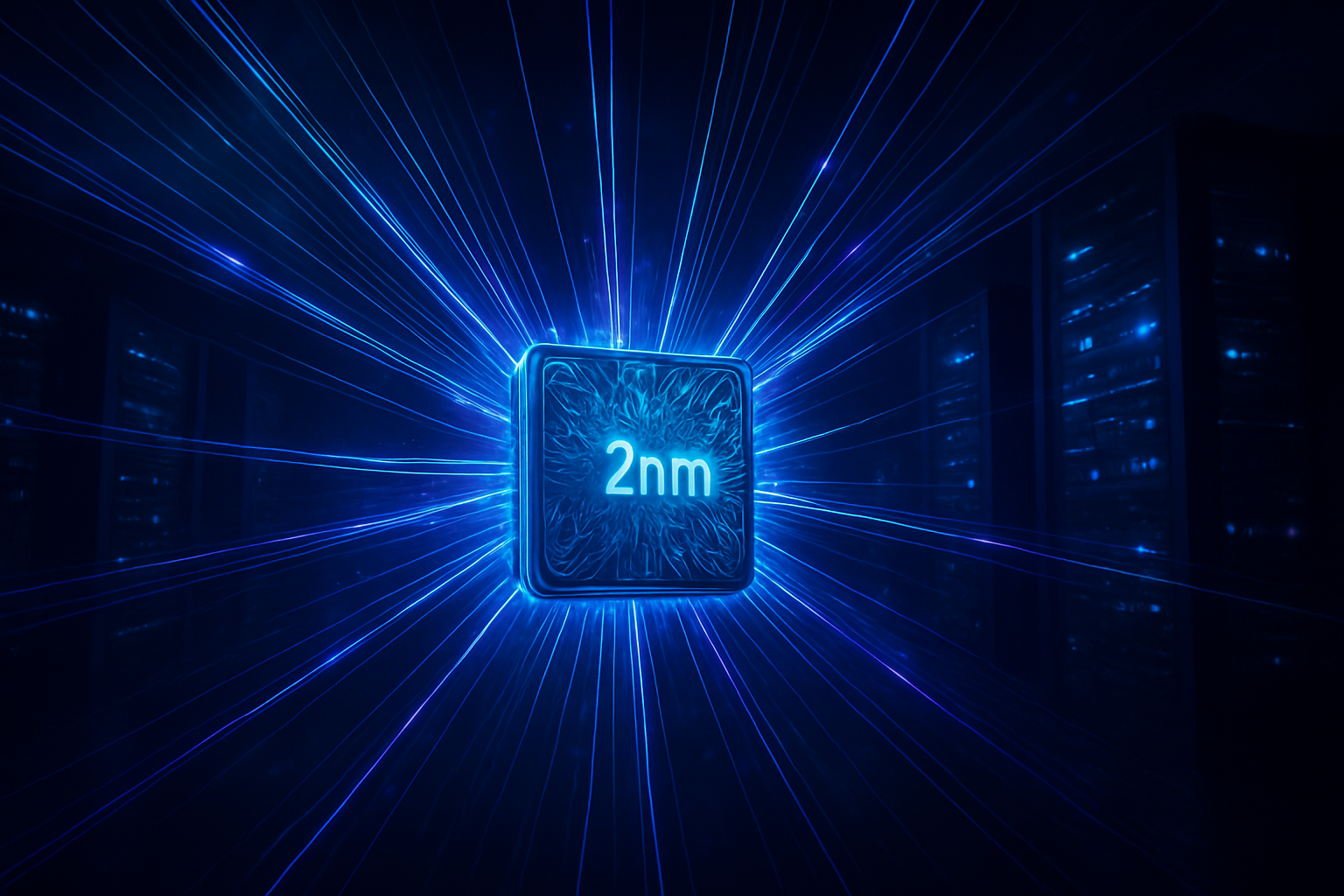
    The technical catalyst for this historic pause is the global shortage of high-density memory modules, a crisis industry analysts are calling "RAMageddon." While the RTX 50-series "Blackwell" cards launched in early 2025 were meant to be followed by a "Super" refresh in early 2026, those plans were scrapped in December 2025. The 3GB GDDR7 modules required for those cards are now being funneled exclusively into the production of NVIDIA’s Rubin R100 and Rubin CPX AI accelerators. These enterprise-grade chips are designed for "massive-context" inference, allowing large language models (LLMs) to process millions of tokens simultaneously—a task that requires every bit of high-performance memory NVIDIA can secure.

    By pushing the consumer version of the Rubin architecture to 2028, NVIDIA is creating an unprecedented three-to-four-year gap between major gaming GPU generations. This is a stark departure from the traditional two-year cadence that defined the PC gaming industry for decades. Furthermore, NVIDIA is reportedly slashing production of current RTX 50-series cards by up to 40% throughout the first half of 2026. This reduction ensures that manufacturing lines at TSMC remain open for the Blackwell Ultra (B300) and upcoming Rubin systems, which command profit margins of 65% or higher, compared to the roughly 40% seen in the gaming sector.

    Initial reactions from the gaming and research communities have been polarized. While AI researchers at institutions like OpenAI and major tech hubs welcome the increased supply of accelerators, PC enthusiasts are mourning the "death of the enthusiast tier." Hardware experts note that without a 2026 refresh, the high-end gaming market will likely stagnate, with existing flagship cards like the RTX 5090 seeing secondary market prices inflate to as much as $5,000 as supply dries up.

    A Vacuum Without a Victor: The Competitive Landscape in 2026

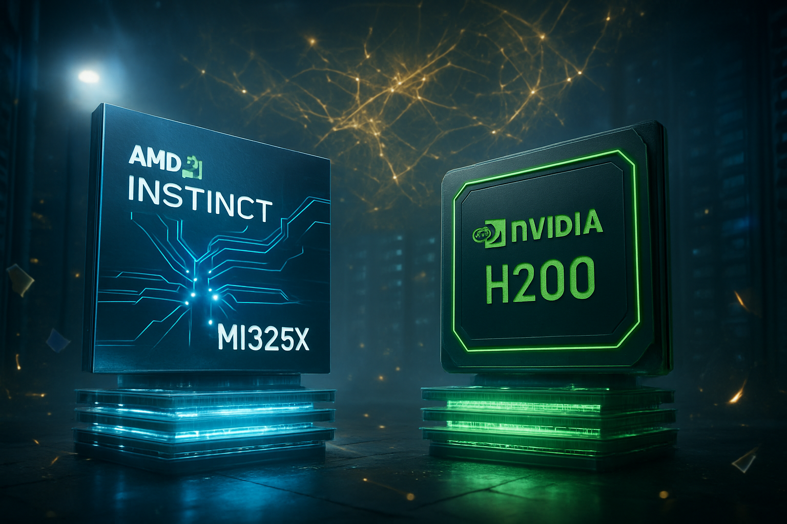
    NVIDIA’s retreat from the high-end gaming market in 2026 might seem like a golden opportunity for competitors like AMD (Nasdaq: AMD) and Intel (Nasdaq: INTC), but both companies are struggling with the same economic and supply-chain realities. AMD has signaled a shift toward "mainstream efficiency," with its RDNA 4 architecture (RX 9000 series) focusing on mid-range affordability rather than challenging NVIDIA’s high-end dominance. Reports suggest that AMD’s own enthusiast-level "UDNA" architecture has also slipped into late 2027, as they too prioritize their Instinct line of AI chips.

    Intel, meanwhile, has faced internal pressure to maintain financial viability in its graphics division. The high-end "Battlemage" B770 discrete GPU was reportedly shelved in early 2026, with the company focusing its "Celestial" (Xe3) architecture primarily on integrated graphics for its Panther Lake processors. This leaves the high-performance desktop market in a state of "hibernation." For the major cloud providers like Microsoft (Nasdaq: MSFT), Amazon (Nasdaq: AMZN), and Alphabet (Nasdaq: GOOGL), NVIDIA’s decision is a victory, ensuring they remain at the front of the line for the silicon necessary to power the next generation of generative AI agents and multi-modal models.

    The AI First Reality: Gaming as a Legacy Business

    This shift is the clearest evidence yet that NVIDIA no longer views itself as a "gaming company." In 2022, gaming accounted for 35% of NVIDIA's revenue; as of early 2026, that figure has dwindled to a mere 8%. The financial logic is inescapable: a single data center rack filled with Rubin GPUs can generate more profit than hundreds of thousands of individual GeForce cards. This transformation mirrors the broader trend in the tech landscape, where "AI First" has moved from a marketing slogan to a brutal operational reality.

    The wider significance of this milestone cannot be overstated. We are witnessing the decoupling of consumer hardware from the bleeding edge of silicon technology. For thirty years, gamers were the primary drivers of GPU innovation, funding the R&D that eventually made AI possible. Now, that relationship has inverted. AI is the driver, and consumer gaming is effectively a "legacy" business that must wait for the scraps of production capacity left over by enterprise demand. This mirrors previous industry shifts, such as the transition from mainframe to personal computing, but in reverse—computing power is being re-centralized into massive "AI Factories."

    The Roadmap to 2028: What Lies Ahead

    Looking toward 2027 and 2028, the challenges for the consumer market are significant. Even when the Rubin-based RTX 60 series eventually arrives in 2028, it is expected to carry a premium price tag to justify the use of data-center-grade memory. Analysts predict that the "mid-range" of the future will rely heavily on AI-driven upscaling and frame generation to compensate for stagnant hardware performance. The burden of innovation is shifting from hardware to software, with technologies like DLSS 5.0 and neural rendering becoming the primary ways gamers will see visual improvements in the coming years.

    In the near term, the vacuum left by NVIDIA may accelerate the rise of alternative gaming platforms. Handheld PCs and "thin client" cloud gaming services are expected to see a surge in popularity as discrete desktop upgrades become prohibitively expensive. Experts predict that the next two years will be a period of "optimization" rather than "innovation" for game developers, who must now target hardware that is effectively frozen in the 2025 era.

    Closing the Chapter on the Graphics Era

    NVIDIA's decision to skip 2026 is a watershed moment in the history of computing. It marks the definitive end of the "Graphics Era" and the total ascent of the "AI Era." While the news is a bitter pill for the PC gaming community, it represents a bold bet by NVIDIA CEO Jensen Huang that the future of his company—and the global economy—lies in the specialized silicon that powers artificial intelligence.

    As we move through 2026, the industry will be watching for any signs of a production thaw or a pivot from competitors. For now, the message from Santa Clara is clear: the "AI Factory" is running at full capacity, and the world of gaming will have to wait its turn.


    This content is intended for informational purposes only and represents analysis of current AI developments.

    TokenRing AI delivers enterprise-grade solutions for multi-agent AI workflow orchestration, AI-powered development tools, and seamless remote collaboration platforms.
    For more information, visit https://www.tokenring.ai/.

  • The Bespoke Brain: How Marvell is Architecting the Custom Silicon Revolution to Dethrone the General-Purpose GPU

    The Bespoke Brain: How Marvell is Architecting the Custom Silicon Revolution to Dethrone the General-Purpose GPU

    As the artificial intelligence landscape shifts from a frantic gold rush for raw compute to a disciplined era of efficiency and scale, Marvell Technology (NASDAQ: MRVL) has emerged as the silent architect behind the world’s most powerful "AI Factories." By February 2026, the era of relying solely on general-purpose GPUs has begun to wane, replaced by a "Custom Silicon Revolution" where cloud titans like Microsoft (NASDAQ: MSFT), Amazon (NASDAQ: AMZN), and Meta Platforms (NASDAQ: META) are bypassing traditional hardware limitations to build bespoke accelerators tailored to their specific neural architectures.

    This transition marks a fundamental shift in the semiconductor industry. While NVIDIA (NASDAQ: NVDA) remains the dominant force in frontier model training, Marvell has carved out a massive, high-margin niche by providing the foundational intellectual property (IP) and specialized interconnects that allow hyperscalers to "de-Nvidia-ize" their infrastructure. Through strategic acquisitions and a relentless push into the 2-nanometer (2nm) manufacturing node, Marvell is now enabling "planet-scale" computing, where custom-built XPUs (AI Accelerators) operate with efficiencies that standard chips simply cannot match.

    Engineering the 2nm AI Fabric: Chiplets, Optics, and HBM4

    At the heart of Marvell’s dominance is its 2nm data infrastructure platform, which entered high-volume production in late 2025. Unlike traditional monolithic chips, Marvell utilizes a modular "chiplet" architecture. This approach allows cloud providers to mix and match high-performance compute dies with specialized I/O and memory controllers. By separating these functions, Marvell can integrate the latest HBM4 memory interfaces and 1.6T optical interconnects onto a single package, offering a level of customization that was previously impossible.

    A critical technical breakthrough driving this revolution is Marvell’s integration of "Photonic Fabric" technology, bolstered by its 2025 acquisition of Celestial AI. In 2026, this technology has begun replacing traditional copper wiring with optical I/O directly at the chip level. This enables vertical (3D) co-packaging of optics, delivering a staggering 16 Terabits per second (Tbps) of bandwidth per chiplet with latency below 150 nanoseconds. This solves the "interconnect bottleneck" that has long plagued multi-GPU clusters, allowing 100,000-node clusters to function as a single, unified processor.

    Furthermore, Marvell’s custom silicon approach addresses the "Memory Wall"—the physical limit of how much data can be fed to a processor. By utilizing Compute Express Link (CXL) 3.0 via their Structera™ line, Marvell-designed accelerators can pool terabytes of external memory across entire server racks. This capability is essential for 2026-era "agentic" AI models, which require massive amounts of memory to maintain "reasoning" state across long-running tasks, a feat that standard GPUs struggle to achieve without excessive power consumption.

    The TCO War: Why Hyperscalers are Turning Away from 'Silicon Cruft'

    The strategic move toward custom silicon is driven by a ruthless focus on Total Cost of Ownership (TCO). General-purpose GPUs, such as NVIDIA’s Blackwell and the newly released Rubin architecture, are designed to be "jack-of-all-trades," carrying legacy hardware for scientific simulation and graphics rendering that go unused in AI inference. This "silicon cruft" leads to higher power draws—often exceeding 1,000 watts per chip—and inflated costs.

    By partnering with Marvell, companies like Amazon and Microsoft are stripping away non-essential logic to create "surgically specialized" chips. For instance, Amazon’s Trainium 3 and Microsoft’s Maia 300—both developed with Marvell’s IP—are optimized for specific Microscaling (MX) data formats. These custom designs offer a 30% to 50% improvement in performance-per-watt over general-purpose alternatives. In a world where electricity has become the primary constraint on AI expansion, this efficiency is the difference between a profitable service and a loss-leader.

    The competitive implications are profound. While Broadcom (NASDAQ: AVGO) remains the leader in the custom ASIC market through its long-standing ties with Alphabet (NASDAQ: GOOGL) and OpenAI, Marvell has successfully positioned itself as the "agile challenger." Marvell’s recent wins with Meta for Data Processing Units (DPUs) and its role as the primary silicon partner for Microsoft’s Maia initiative have propelled its AI-related revenue past $3.5 billion annually, representing over 70% of its data center business.

    Beyond the GPU: A Paradigm Shift in AI Hardware

    The broader significance of Marvell’s role lies in the democratization of silicon design. Historically, only a handful of firms had the expertise to design world-class processors. Marvell’s "Building Block" approach has changed the landscape, providing cloud giants with the pre-verified IP—from 448G SerDes to ARM-based compute subsystems—needed to bring their own silicon to life in record time. This shift is turning the semiconductor industry from a product-based market into a service-based one, where "Silicon-as-a-Service" is the new norm.

    This trend also highlights a growing divide in the AI industry. While NVIDIA continues to lead the "training" market, where raw horsepower is king, the "inference" market—where models are actually run for users—is rapidly moving toward custom silicon. This is because inference requires low latency and high throughput at the lowest possible power cost. Marvell’s focus on the "XPU-attached" market—the networking and memory links that surround the compute core—has made them indispensable regardless of whose name is on the front of the chip.

    However, this revolution is not without its challenges. The shift to 2nm and the integration of complex optical packaging have pushed the limits of global supply chains. Reliance on TSMC (NYSE: TSM) for advanced manufacturing remains a single point of failure for the entire industry. Additionally, as cloud providers build their own "walled gardens" of custom silicon, the industry faces potential fragmentation, where software optimized for one cloud titan’s custom chip may not run efficiently on another’s.

    The Road to 'Planet-Scale' Computing and 1.6T Optics

    Looking ahead, the next 24 months will see the full deployment of 1.6T and 3.2T optical links, technologies where Marvell holds a commanding lead with its Nova 2 PAM4 DSPs. These speeds are necessary to support the "million-GPU" clusters currently being planned by the largest AI labs. As models continue to scale toward 100-trillion parameters, the focus will shift entirely from individual chip performance to the efficiency of the "system-on-a-rack."

    Experts predict that by 2027, the majority of AI inference will happen on custom ASICs rather than merchant GPUs. Marvell is already preparing for this by finalizing the design for the Maia 300 and Trainium 4, which are expected to utilize HBM4 and potentially move toward 1.4nm nodes. The integration of XConn Technologies, acquired by Marvell in early 2026, will further cement their lead in CXL memory pooling, allowing for AI systems with "infinite" memory capacity.

    The next major hurdle will be the software layer. As hardware becomes more specialized, the industry must develop a unified software stack—likely based on the Triton or OpenXLA frameworks—to ensure that developers can target these bespoke chips without rewriting their entire codebases. Marvell’s participation in the Ultra Accelerator Link (UALink) and Ultra Ethernet Consortium (UEC) will be pivotal in establishing these open standards.

    Summary

    Marvell’s transformation from a networking and storage company into the backbone of the custom silicon revolution is one of the most significant pivots in recent tech history. By focusing on the "connective tissue" of the AI factory—high-speed interconnects, optical DSPs, and custom memory fabrics—Marvell has made itself as vital to the AI era as the compute cores themselves.

    As of February 2026, the key takeaway is that the "GPU-only" era of AI has ended. The future belongs to those who can build the most efficient, workload-specific systems. Marvell’s role as the primary enabler for the cloud titans ensures that it will remain at the center of the AI ecosystem for years to come. In the coming months, investors and analysts should watch for the first production benchmarks of the 2nm Maia 300 and the rollout of the first "Photonic Fabric" clusters, as these will define the next benchmark for AI performance and efficiency.


    This content is intended for informational purposes only and represents analysis of current AI developments.

    TokenRing AI delivers enterprise-grade solutions for multi-agent AI workflow orchestration, AI-powered development tools, and seamless remote collaboration platforms.
    For more information, visit https://www.tokenring.ai/.

  • The 6-Micron Leap: How TSMC’s Hybrid Bonding Revolution is Powering the Next Generation of AI Supercomputers

    The 6-Micron Leap: How TSMC’s Hybrid Bonding Revolution is Powering the Next Generation of AI Supercomputers

    As of February 5, 2026, the semiconductor industry has officially entered the era of "Bumpless" silicon. The long-anticipated transition from traditional solder-based microbumps to direct copper-to-copper (Cu-Cu) hybrid bonding has reached a critical tipping point, with Taiwan Semiconductor Manufacturing Co. (NYSE: TSM) announcing that its System on Integrated Chips (SoIC) technology has successfully achieved high-volume manufacturing (HVM) at a 6-micrometer bond pitch. This milestone represents a tectonic shift in how the world’s most powerful processors are built, moving beyond the physical limits of two-dimensional scaling into a fully integrated 3D landscape.

    The immediate significance of this development cannot be overstated. By eliminating the bulky solder "bumps" that have connected chips for decades, TSMC has unlocked a 100x increase in interconnect density and a dramatic reduction in power consumption. This breakthrough serves as the foundational architecture for the industry’s most ambitious AI accelerators, including the newly debuted NVIDIA (NASDAQ: NVDA) Rubin series and the AMD (NASDAQ: AMD) Instinct MI400. In an era where AI training clusters consume gigawatts of power, the ability to move data between logic and memory with nearly zero resistance is no longer a luxury—it is a requirement for the continued survival of Moore’s Law.

    The Death of the Microbump: Engineering the 6-Micrometer Interface

    At the heart of this revolution is TSMC’s SoIC-X (bumpless) technology. For years, the industry relied on "microbumps"—tiny spheres of solder roughly 30 to 40 micrometers in diameter—to stack chips. However, as AI models grew, these bumps became a bottleneck; they were too large to allow for the thousands of simultaneous connections required for high-bandwidth data transfer and contributed significant electrical parasitics. TSMC’s 6-micrometer hybrid bonding process replaces these bumps with a direct, atomic-level fusion of copper pads. The process begins with Chemical Mechanical Polishing (CMP) to achieve a surface flatness with less than 0.5 nanometers of roughness, followed by plasma activation of the dielectric surface. When two wafers are pressed together at room temperature and subsequently annealed at 200°C, the copper pads expand and fuse into a single, continuous metal path.

    This "bumpless" architecture allows for a staggering density of 25,000 to 50,000 interconnects per square millimeter, compared to the roughly 600–1,000 interconnects possible with standard microbumps. By shrinking the bond pitch to 6 micrometers, TSMC has effectively turned 3D chip stacks into a single, monolithic piece of silicon from an electrical perspective. Initial reactions from the AI research community have been electric, with experts noting that the vertical distance between dies is now so small that signal latency has effectively vanished, allowing for "logic-on-logic" stacking that behaves as if it were a single, giant processor.

    The technical specifications of this leap are already manifesting in hardware. The NVIDIA Rubin platform, announced just weeks ago, utilizes this 6µm SoIC-X architecture to integrate the "Vera" CPU and "Rubin" GPU with HBM4 memory. Because HBM4 uses a 2048-bit interface—double the width of the previous generation—it is physically incompatible with legacy microbump technology. Hybrid bonding is the only way to accommodate the sheer number of pins required to hit Rubin’s target memory bandwidth of 13 TB/s.

    The Interconnect War: Market Dominance in Foundry 2.0

    The successful scaling of 6µm hybrid bonding has solidified TSMC’s lead in what analysts are calling "Foundry 2.0"—a market where packaging is as important as transistor size. According to recent data from IDC, TSMC’s market share in advanced packaging is projected to reach 66% by the end of 2026. This dominance is driven by the fact that both NVIDIA and AMD have pivoted their entire flagship roadmaps to favor TSMC’s SoIC ecosystem. AMD’s Instinct MI400, built on the CDNA 5 architecture, leverages SoIC to stack a massive 432GB of HBM4 memory directly over its compute dies, achieving a "yotta-scale" foundation that AMD claims is 50% more dense than its previous generation.

    However, the competition is not standing still. Intel (NASDAQ: INTC) is aggressively pushing its "Foveros Direct" technology, aiming to reach a sub-5-micrometer pitch by the second half of 2026 on its 18A-PT node. Intel’s strategy involves combining hybrid bonding with its "PowerVia" backside power delivery, a dual-pronged attack intended to win back hyperscaler customers like Microsoft (NASDAQ: MSFT) and Amazon (NASDAQ: AMZN) who are designing custom AI silicon. Meanwhile, Samsung Electronics (KRX: 005930) has launched its SAINT (Samsung Advanced Interconnect Technology) platform, specifically targeting the integration of its own HBM4 modules with logic dies in a "one-stop-shop" model that could appeal to cost-conscious AI labs.

    The competitive implications are stark: companies unable to master hybrid bonding at the 6µm level or below risk being relegated to the mid-tier market. The strategic advantage for TSMC lies in its mature "3DFabric" ecosystem, which provides a standardized design flow for chiplet-based architectures. This has forced a shift in the industry where the "interconnect" is now the primary theater of competition, rather than the transistor gate itself.

    Breaking the Memory Wall and the Power Efficiency Frontier

    Beyond the corporate horse race, the hybrid bonding revolution addresses the two greatest crises in modern computing: the "Memory Wall" and the "Power Wall." For years, CPU and GPU speeds have outpaced the ability of memory to supply data, leading to wasted cycles and energy. By using 6µm hybrid bonding, designers can place memory directly on top of logic, reducing the distance data must travel from millimeters to micrometers. This results in a power efficiency of less than 0.05 picojoules per bit (pJ/bit)—a 3x to 10x improvement over 2.5D technologies like CoWoS and orders of magnitude better than traditional flip-chip packaging.

    This shift fits into a broader trend of "Extreme Co-Design," where software, architecture, and packaging are developed in tandem. In the wider AI landscape, this means that the trillion-parameter models of 2026 can be trained on clusters that are physically smaller and significantly more energy-efficient than the massive data centers of the early 2020s. However, this advancement is not without concerns. The extreme precision required for 6µm bonding makes these chips incredibly difficult to repair; a single misaligned bond during the 200°C annealing process can result in the loss of multiple high-value dies, potentially keeping costs high for several more years.

    Furthermore, the environmental impact of this technology is a double-edged sword. While the pJ/bit efficiency is a victory for sustainability, the increased performance is expected to trigger "Jevons Paradox," where the improved efficiency leads to an even greater total demand for AI compute, potentially offsetting any net energy savings at the global level.

    Looking Ahead: The Path to 3 Micrometers and Beyond

    The 6-micrometer milestone is merely a pitstop on TSMC’s roadmap. The company has already demonstrated prototypes of its "SoIC-Next" generation, which targets a 3-micrometer bond pitch for 2027. Experts predict that at the 3µm level, we will see the birth of "True 3D" processors, where different tiers of a single logic core are stacked on top of each other, allowing for clock speeds that were previously thought impossible due to thermal constraints.

    We are also likely to see the emergence of an open chiplet ecosystem. With the implementation of the UCIe 2.0 (Universal Chiplet Interconnect Express) standard, 2026 and 2027 could see the first "mix-and-match" 3D stacks, where a specialized AI accelerator tile from a startup could be hybrid-bonded directly onto a base die from Intel or TSMC. The challenges remaining are primarily around thermal management and testing. Stacking multiple layers of high-power logic creates a "heat sandwich" that requires advanced liquid cooling or integrated microfluidic channels—technologies that are currently in the experimental phase but will become mandatory as we move toward 3µm pitches.

    A New Dimension for Artificial Intelligence

    The achievement of 6-micrometer hybrid bonding marks the definitive end of the "2D Silicon" era. In the history of artificial intelligence, this transition will likely be remembered as the moment when hardware finally caught up to the structural demands of neural networks. By mimicking the dense, three-dimensional connectivity of the human brain, hybrid-bonded chips are providing the physical substrate necessary for the next leap in machine intelligence.

    In the coming months, the industry will be watching the yield rates of the NVIDIA Rubin and AMD MI400 very closely. If TSMC can maintain high yields at 6µm, the transition to 3D-first design will become irreversible, forcing a total reorganization of the semiconductor supply chain. For now, the "bumpless" revolution has given the AI industry a much-needed breath of fresh air, proving that even as we reach the atomic limits of the transistor, human ingenuity can always find another dimension in which to grow.


    This content is intended for informational purposes only and represents analysis of current AI developments.

    TokenRing AI delivers enterprise-grade solutions for multi-agent AI workflow orchestration, AI-powered development tools, and seamless remote collaboration platforms.
    For more information, visit https://www.tokenring.ai/.

  • The Glass Age: Semiconductor Breakthrough Shatters the ‘Warpage Wall’ for Next-Gen AI Accelerators

    The Glass Age: Semiconductor Breakthrough Shatters the ‘Warpage Wall’ for Next-Gen AI Accelerators

    The semiconductor industry has officially entered a new era. As of February 2026, the long-predicted transition from organic packaging materials to glass substrates has moved from laboratory curiosity to a critical manufacturing reality. This shift marks the first major departure in decades from Ajinomoto Build-up Film (ABF), the industry-standard organic resin that has underpinned chip packaging since the 1990s. The move is not merely an incremental upgrade; it is a desperate and necessary response to the "Warpage Wall," a physical limitation that threatened to halt the scaling of the world’s most powerful AI accelerators.

    For companies like NVIDIA Corporation (NASDAQ: NVDA) and Advanced Micro Devices, Inc. (NASDAQ: AMD), the glass breakthrough is the "oxygen" required for their next generation of hardware. By replacing organic cores with ultra-rigid glass, manufacturers are now able to package massive, multi-die chiplets that would have physically buckled under the heat and pressure of traditional manufacturing. This month, the first production-grade AI modules featuring glass-based architectures have begun shipping, signaling a fundamental change in how the silicon brains of the AI revolution are built.

    Shattering the Warpage Wall: The Technical Leap Forward

    The technical driver behind this transition is a phenomenon known as the "Warpage Wall." As AI accelerators grow larger to accommodate more transistors and High Bandwidth Memory (HBM), the thermal expansion differences between silicon and organic ABF substrates become catastrophic. At the extreme operating temperatures of modern data centers, organic materials expand and contract at rates far different from the silicon chips they support. This leads to "warping"—a physical bending of the package that snaps microscopic interconnects and craters manufacturing yields. Glass, however, possesses a Coefficient of Thermal Expansion (CTE) that nearly matches silicon. This thermal harmony allows for a 50% reduction in warpage, enabling the creation of packages that are twice the size of current lithography limits, reaching up to 1,700 mm².

    Beyond thermal stability, glass offers a level of flatness that organic materials cannot replicate. Glass substrates are approximately three times flatter than their organic counterparts, providing a superior foundation for advanced lithography. This extreme flatness allows for the deployment of ultra-fine Redistribution Layers (RDL) with features smaller than 2µm. Furthermore, glass is an exceptional insulator with a low dielectric constant, which reduces signal interference and power loss. Early benchmarks from February 2026 indicate that chips using glass substrates are achieving a 30% to 50% improvement in power efficiency—a critical metric for the power-hungry AI industry.

    The "holy grail" of this advancement is the Through-Glass Via (TGV). While traditional organic substrates rely on mechanical drilling that is limited to a roughly 325µm pitch, glass allows for laser-induced etching to create vias at a pitch of 100µm or less. Because density scales quadratically with pitch, this move from 325µm to 100µm delivers a staggering 10.56x increase in interconnect density. This enables up to 50,000 I/O connections per package, providing the massive vertical power delivery and data throughput required by the high-current demands of the newest GPU architectures.

    The Corporate Race for Glass Supremacy

    The competitive landscape of the semiconductor industry has been jolted by this transition, with Intel Corporation (NASDAQ: INTC) currently leading the charge. In late January 2026, Intel unveiled its first mass-market CPU featuring a glass core, the Xeon 6+ "Clearwater Forest." This achievement followed years of R&D at its Chandler, Arizona facility. By successfully implementing a "thick-core" 10-2-10 architecture—ten RDL layers on each side of a 1.6mm glass core—Intel has positioned itself as the primary architect of the glass era, leveraging its internal packaging capabilities to gain a strategic advantage over competitors who rely solely on external foundries.

    However, the competition is fierce. SK Hynix Inc. (KRX: 000660), through its specialized subsidiary Absolics, has become the first to achieve large-scale commercialization for third-party clients. Operating out of a new $600 million facility in Georgia, USA, Absolics is already supplying glass substrate samples to AMD and Amazon.com, Inc. (NASDAQ: AMZN) for their custom AI silicon. Meanwhile, Samsung Electronics (KRX: 000660) has mobilized its "Triple Alliance"—integrating its electronics, display, and electro-mechanics divisions—to accelerate its own glass production. Samsung shifted its glass project to a dedicated Commercialization Unit this month, aiming to capture the high-end System-in-Package (SiP) market by the end of 2026.

    Taiwan Semiconductor Manufacturing Company (NYSE: TSM) is taking a slightly different but equally ambitious path. TSMC is focusing on Panel-Level Packaging (PLP) using rectangular glass panels as large as 750x620mm. This approach, known as CoPoS (Chip-on-Panel-on-Substrate), aims to maximize area utilization and lower costs for the massive scale required by the upcoming "Vera Rubin" architecture from NVIDIA. While Intel and SK Hynix are ahead in immediate deployments, TSMC’s panel-level scale could define the cost structure of the industry by 2027 and 2028.

    A Fundamental Shift in the AI Landscape

    The adoption of glass substrates is more than a packaging upgrade; it is the physical realization of "More than Moore." As traditional transistor scaling slows down, the industry has turned to "system-level" scaling. Glass provides the rigid backbone necessary to stitch together dozens of chiplets into a single, massive compute engine. Without glass, the thermal and mechanical stresses of modern AI chips would have hit a hard ceiling, potentially stalling the progress of Large Language Models (LLMs) and generative AI research that depends on ever-more-powerful hardware.

    This breakthrough also has significant implications for data center efficiency and environmental sustainability. The 30-50% reduction in power consumption afforded by glass’s superior electrical properties arrives at a time when AI energy demand is under intense global scrutiny. By reducing signal loss and improving thermal management, glass substrates allow data centers to pack more compute density into the same physical footprint without an exponential increase in cooling requirements. This makes the "Glass Age" a pivotal moment in the transition toward more sustainable high-performance computing.

    However, the transition is not without its risks. The move to glass requires a complete overhaul of the packaging supply chain. Traditional substrate makers who cannot pivot from organic materials risk obsolescence. Furthermore, the brittleness of glass poses unique handling challenges during the manufacturing process, and while yields are improving—Absolics reports levels between 75% and 85%—they still lag behind the mature organic processes of yesteryear. The industry is effectively "re-learning" how to build chips, a process that carries significant capital risk.

    The Horizon: From AI Accelerators to Optical Integration

    Looking ahead, the roadmap for glass substrates extends far beyond simple GPU packaging. Experts predict that by 2028, the industry will begin integrating Co-Packaged Optics (CPO) directly onto glass substrates. Because glass is transparent and can be etched with high precision, it is the ideal medium for routing both electrical signals and light. This could lead to a future where chip-to-chip communication happens via on-package lasers and waveguides, virtually eliminating the latency and power bottlenecks of copper wiring.

    We also expect to see "Glass-First" designs for consumer electronics. While the current focus is on $40,000 AI GPUs, the mechanical benefits of glass—allowing for thinner, more rigid, and more thermally efficient devices—will eventually trickle down to high-end laptops and smartphones. As manufacturing yields stabilize throughout 2026 and 2027, the "Glass Age" will move from the data center to the pocket. The next milestone to watch will be the full-scale deployment of NVIDIA’s Rubin platform, which is expected to be the ultimate proof-of-concept for the viability of glass at the highest levels of global computing.

    Conclusion: A New Foundation for Intelligence

    The breakthrough of glass substrates in February 2026 marks a watershed moment in semiconductor history. By overcoming the "Warpage Wall," the industry has cleared the path for the next decade of AI scaling, ensuring that the physical limitations of organic materials do not hinder the digital aspirations of the AI research community. The transition reflects a broader trend in the tech industry: when software demands reach the limits of physics, the industry innovates its way into entirely new materials.

    As we look toward the remainder of 2026, the primary indicators of success will be the production yields at the new glass facilities in Arizona and Georgia, and the thermal performance of the first "Clearwater Forest" and "Rubin" chips in the wild. The silicon era has not ended, but it has found a new, clearer foundation. The "Glass Age" is no longer a future prediction—it is the operational reality of the global AI economy.


    This content is intended for informational purposes only and represents analysis of current AI developments.

    TokenRing AI delivers enterprise-grade solutions for multi-agent AI workflow orchestration, AI-powered development tools, and seamless remote collaboration platforms.
    For more information, visit https://www.tokenring.ai/.

  • The CoWoS Crunch: Why TSMC’s Specialized Packaging Remains the AI Industry’s Ultimate Bottleneck

    The CoWoS Crunch: Why TSMC’s Specialized Packaging Remains the AI Industry’s Ultimate Bottleneck

    As of February 2, 2026, the global artificial intelligence landscape remains in the grip of an "AI super-cycle," where the ability to deploy large-scale models is limited not by software ingenuity, but by the physical architecture of silicon. At the center of this storm is Taiwan Semiconductor Manufacturing Co. (NYSE: TSM), whose advanced packaging technology, Chip-on-Wafer-on-Substrate (CoWoS), has become the single most critical bottleneck in the production of next-generation AI accelerators. Despite a massive capital expenditure push and the rapid commissioning of new facilities, the demand for CoWoS capacity continues to stretch the limits of the semiconductor supply chain.

    The current constraints are driven by the transition to increasingly complex chip architectures, such as NVIDIA’s (NASDAQ: NVDA) Blackwell and the newly debuted Rubin series, which require sophisticated 2.5D and 3D integration to function. While TSMC has successfully scaled its monthly output to record levels, the sheer volume of orders from hyperscalers and chip designers has created a persistent backlog. For the industry's titans, the race for AI dominance is no longer just about who has the best algorithms, but who has secured the most "slots" on TSMC's packaging lines for 2026 and beyond.

    Bridging the Gap: The Technical Evolution of CoWoS-L and CoWoS-S

    At its core, CoWoS is a high-density packaging technology that allows multiple chips—typically a Logic GPU or ASIC alongside several stacks of High Bandwidth Memory (HBM)—to be integrated onto a single substrate. This proximity is vital for AI workloads, which require massive data throughput between the processor and memory. In 2026, the technical challenge has shifted from the traditional CoWoS-S (using a silicon interposer) to the more complex CoWoS-L. This newer variant utilizes Local Silicon Interconnect (LSI) bridges to link multiple active dies, enabling chips that are physically larger than the traditional reticle limit of a single silicon wafer.

    This shift is essential for NVIDIA’s B200 and GB200 Blackwell chips, which effectively act as dual-die processors. The precision required to align these components at the micron level is immense, leading to lower initial yields compared to standard chip manufacturing. Industry experts note that while CoWoS-S was sufficient for the previous H100 generation, the "multi-die" era of 2026 demands the flexibility of CoWoS-L. This complexity is why TSMC’s utilization rates remain at near 100% despite the company’s efforts to automate and expand its Advanced Backend (AP) facilities.

    The Hierarchy of Chips: Who Wins the Capacity War?

    The scramble for packaging capacity has created a clear hierarchy in the semiconductor market. NVIDIA remains the "anchor tenant," reportedly securing roughly 60% of TSMC’s total CoWoS output for the 2026 fiscal year. This dominance has allowed NVIDIA to maintain its lead with the Blackwell series, even as it prepares the 3nm-based Rubin architecture for mass production. However, Advanced Micro Devices (NASDAQ: AMD) has made significant inroads, securing approximately 11% of capacity for its Instinct MI350 and MI400 series, which compete directly for high-end enterprise deployments.

    Beyond the GPU giants, the "Sovereign AI" movement has seen companies like Alphabet Inc. (NASDAQ: GOOGL) and Amazon.com Inc. (NASDAQ: AMZN) bypass standard chip vendors to design their own custom ASICs. Google’s TPU v6 and Amazon’s Trainium 3 chips are now major consumers of CoWoS capacity, often facilitated through design partners like MediaTek (TWSE: 2454). This influx of custom silicon has intensified the competition, forcing smaller AI startups to look toward secondary providers or wait in line for the "spillover" capacity handled by Outsourced Semiconductor Assembly and Test (OSAT) firms like ASE Technology Holding (NYSE: ASX) and Amkor Technology (NASDAQ: AMKR).

    A Global Shift: Beyond the Taiwan Bottleneck

    The CoWoS shortage has sparked a broader conversation about the geographical concentration of advanced packaging. Historically, almost all of TSMC’s advanced packaging was centralized in Taiwan. However, the 2026 landscape shows the first signs of a decentralized model. TSMC’s AP8 facility in Tainan and the newly operational AP7 in Chiayi have been the primary drivers of growth, but the company has recently confirmed plans to establish an advanced packaging hub in Arizona by 2027. This move is seen as a direct response to pressure from the U.S. government to secure a domestic supply chain for critical AI infrastructure.

    Furthermore, the industry is grappling with a secondary bottleneck: High Bandwidth Memory. Even as TSMC expands CoWoS lines, the supply of HBM3e and the emerging HBM4 from vendors like Samsung Electronics (KRX: 005930) is struggling to keep pace. This dual-constraint environment—where both the packaging and the memory are in short supply—has led to a "packaging-bound" era of chip manufacturing. The result is a market where the cost of AI hardware remains high, and the lead times for AI server clusters can still stretch into several months.

    The Road to 2027: Silicon Photonics and HBM4

    Looking ahead, the industry is already preparing for the next technical leap. Predictions for 2027 suggest that CoWoS will evolve to incorporate Silicon Photonics, a technology that uses light instead of electricity to transfer data between chips. This would significantly reduce power consumption—a major concern for data centers currently struggling with the multi-kilowatt demands of Blackwell-based racks. TSMC is reportedly in the early stages of integrating "CPO" (Co-Packaged Optics) into its CoWoS roadmap to address these thermal and power limits.

    Additionally, the transition to HBM4 in late 2026 and 2027 will require even more precise packaging techniques, as the memory stacks move to 12-layer and 16-layer configurations. This will likely keep the pressure on TSMC to continue its aggressive capital investment. Analysts predict that while the extreme supply-demand imbalance may ease slightly by the end of 2026 as Phase 2 of the Chiayi plant reaches full capacity, the long-term trend remains one of hyper-growth, with AI packaging expected to contribute more than 10% of TSMC's total revenue in the coming years.

    Summary: A Redefined Semiconductor Landscape

    The ongoing CoWoS capacity constraints at TSMC have fundamentally redefined what it means to be a chipmaker in the AI era. No longer is it enough to have a brilliant circuit design; companies must now master the intricacies of "System-in-Package" (SiP) logistics and secure a reliable place in the packaging queue. TSMC’s response—building a million-wafer-per-year capacity by the end of 2026—is a testament to the unprecedented scale of the AI revolution.

    As we move through 2026, the industry will be watching for two key indicators: the yield rates of CoWoS-L at the new AP8 facility and the speed at which OSAT partners can absorb the overflow for mid-tier AI applications. For now, the "CoWoS Crunch" remains the defining challenge of the hardware world, a physical limit on the digital aspirations of the world’s most powerful AI models.


    This content is intended for informational purposes only and represents analysis of current AI developments.

    TokenRing AI delivers enterprise-grade solutions for multi-agent AI workflow orchestration, AI-powered development tools, and seamless remote collaboration platforms.
    For more information, visit https://www.tokenring.ai/.

  • Silicon Sovereignty: Microsoft Taps Intel’s 18A-P Node for Next-Gen Maia 2 AI Accelerators

    Silicon Sovereignty: Microsoft Taps Intel’s 18A-P Node for Next-Gen Maia 2 AI Accelerators

    In a landmark move that signals a tectonic shift in the global semiconductor landscape, Microsoft Corp. (NASDAQ:MSFT) has officially become the flagship foundry customer for Intel Corporation’s (NASDAQ:INTC) most advanced process node to date: the Intel 18A-P. Announced in late January 2026, the partnership centers on the domestic production of Microsoft’s custom-designed "Maia 2" AI accelerators. This multi-year agreement marks the first time a major U.S. hyperscaler has committed to manufacturing its most critical AI silicon on American soil using leading-edge transistor technology, a move aimed at insulating the tech giant from the growing geopolitical volatility surrounding traditional manufacturing hubs in East Asia.

    The collaboration is a crowning achievement for Intel’s "IDM 2.0" strategy, which sought to regain the company's manufacturing lead after years of stagnation. By securing Microsoft as a primary customer, Intel has not only validated its 1.8nm-class technology but has also provided a blueprint for the future of "Silicon-to-Service" integration. For Microsoft, the transition to Intel’s Arizona and Ohio facilities represents a strategic pivot toward supply chain resilience, ensuring that the hardware powering its Azure AI infrastructure remains shielded from the trade disputes and logistics bottlenecks that have plagued the industry in recent years.

    High-Performance Silicon: Inside the 18A-P Node and Maia 2

    The technical cornerstone of this partnership is the Intel 18A-P node, a "Performance-enhanced" version of Intel’s 1.8nm process. The 18A-P node introduces the third generation of RibbonFET, Intel’s implementation of Gate-All-Around (GAA) transistor architecture. This design offers superior electrostatic control, which drastically reduces power leakage while enabling higher drive currents. Perhaps more significantly, the node utilizes PowerVia—Intel’s industry-first backside power delivery system. By moving the power delivery network to the back of the wafer, Intel has effectively eliminated signal-to-power interference on the front side, resulting in a reported 10% improvement in cell utilization and a significant reduction in resistive power droops.

    The "Maia 2" (specifically the Maia 200 series) is the first major beneficiary of these architectural gains. Compared to its predecessor, the Maia 100, the new chip boasts a staggering 144 billion transistors—up from 105 billion. It is engineered to deliver 10 petaFLOPS of FP4 compute, a threefold increase in inference performance. To support the massive data throughput required for modern Large Language Models (LLMs), Microsoft has equipped the Maia 2 with 216GB of HBM3e memory, providing a 7TB/s bandwidth that dwarfs the 1.8TB/s seen in the previous generation. Industry experts note that the 18A-P node provides an 8% performance-per-watt advantage over the base 18A node, allowing Microsoft to push the Maia 2 to higher clock speeds without exceeding the thermal limits of its liquid-cooled data centers.

    Reshaping the Foundry Landscape: A Threat to the Status Quo

    This partnership has sent ripples through the semiconductor market, placing immediate pressure on Taiwan Semiconductor Manufacturing Company (NYSE:TSMC). For over a decade, TSMC has held a near-monopoly on leading-edge manufacturing, but Intel’s early successful deployment of PowerVia has challenged that dominance. While TSMC remains a critical partner for many of Microsoft’s other components, the shift of the Maia 2—Microsoft’s most strategic AI asset—to Intel 18A-P suggests that the competitive gap has closed. Analysts suggest that TSMC may now feel forced to accelerate its own A16 node, which also features backside power, to prevent further customer attrition.

    For competitors like NVIDIA Corporation (NASDAQ:NVDA) and Advanced Micro Devices, Inc. (NASDAQ:AMD), the Microsoft-Intel alliance creates a complex strategic environment. NVIDIA has increasingly adopted a "co-opetition" stance, utilizing Intel’s advanced packaging services even as it competes in the chip market. AMD, however, remains more heavily dependent on TSMC’s ecosystem. If Intel’s yields at its Arizona Fab 52 and Ohio "Silicon Heartland" sites continue to meet the reported 60% threshold, Microsoft will possess a significant cost and availability advantage. By bypassing the capacity constraints often found at TSMC, Microsoft can scale its AI clusters more aggressively than rivals who remain tethered to the global supply chain's single point of failure.

    Geopolitical Resilience and the CHIPS Act Legacy

    The broader significance of this move cannot be overstated in the context of global trade. The partnership is the most visible fruit of the CHIPS and Science Act, under which Intel received nearly $8 billion in direct funding to revitalize American semiconductor manufacturing. The U.S. government views the domestic production of AI accelerators as a matter of national security, ensuring that the "brains" of the next generation of artificial intelligence are not subject to the territorial tensions in the South China Sea. Microsoft’s decision to fab the Maia 2 in Arizona—and eventually at the massive Ohio site—serves as a hedge against a potential "black swan" event that could halt production in Taiwan.

    Furthermore, this development marks a shift in how tech giants view their role in the hardware stack. By controlling the design of the chip (Maia 2) and the manufacturing location (Intel’s U.S. fabs), Microsoft is pursuing a "full-stack" sovereignty that was previously only seen in the aerospace or defense sectors. This move is expected to influence other Western tech firms to reconsider their reliance on offshore foundries, potentially sparking a wider trend of "reshoring" critical technology. While concerns remain regarding the higher labor costs associated with U.S. manufacturing, the efficiencies gained from Intel’s 18A-P performance and the reduction in geopolitical risk are seen by Microsoft as a price worth paying.

    The Horizon: From Maia 2 to the 'Griffin' Architecture

    Looking ahead, the road doesn't end with the Maia 2. Microsoft and Intel are already reportedly collaborating on the architectural definitions for a successor, codenamed "Griffin" (likely the Maia 3), which is expected to leverage even more advanced iterations of the 18A-P node. Future developments will likely focus on heterogeneous integration, using Intel’s Foveros Direct 3D packaging to stack memory and compute in even more dense configurations. As Intel’s Ohio facilities come online later this decade, the scale of this partnership is expected to double, providing a massive domestic footprint for AI silicon.

    The primary challenge remaining for Intel is maintaining the yield and consistency of the 18A-P node as it scales to high-volume manufacturing for multiple clients. If Intel can prove it can handle the volume of a client as large as Microsoft without the delays that hampered its 10nm and 7nm transitions, it will firmly re-establish itself as the world’s premier foundry. Experts predict that in the coming months, other "Big Tech" players, potentially including Apple Inc. (NASDAQ:AAPL), may follow Microsoft’s lead in diversifying their foundry partners to include Intel’s domestic sites.

    A New Era of AI Infrastructure

    The announcement of Microsoft as the flagship customer for Intel’s 18A-P node is a defining moment for the AI era. It represents the convergence of high-performance computing, national security, and corporate strategy. By bringing the production of the Maia 2 to Arizona and Ohio, Microsoft has secured a vital link in its supply chain, ensuring that the rapid evolution of its AI services can continue unabated by external geopolitical shocks.

    For Intel, this is the validation the company has sought for nearly five years. The 18A-P node is no longer a theoretical roadmap item; it is a functioning, high-volume manufacturing platform that has attracted one of the world's most valuable companies. As we move into 2026, the industry will be watching closely to see how the first batch of Maia 2 chips performs in the wild. If they deliver on the promised 3x inference boost and the 8% power efficiency gain, the era of Intel’s foundry leadership will have officially begun, fundamentally altering the power dynamics of the global tech industry.


    This content is intended for informational purposes only and represents analysis of current AI developments.

    TokenRing AI delivers enterprise-grade solutions for multi-agent AI workflow orchestration, AI-powered development tools, and seamless remote collaboration platforms.
    For more information, visit https://www.tokenring.ai/.

  • Custom Silicon Titans: Meta and Microsoft Challenge NVIDIA’s Dominance

    Custom Silicon Titans: Meta and Microsoft Challenge NVIDIA’s Dominance

    As of January 26, 2026, the artificial intelligence industry has reached a pivotal turning point in its infrastructure evolution. Microsoft (NASDAQ: MSFT) and Meta Platforms (NASDAQ: META) have officially transitioned from being NVIDIA’s (NASDAQ: NVDA) largest customers to its most formidable architectural rivals. With today's simultaneous milestones—the wide-scale deployment of Microsoft’s Maia 200 and Meta’s MTIA v3 "Santa Barbara" accelerator—the era of the "General Purpose GPU" dominance is being challenged by a new age of hyperscale custom silicon.

    This shift represents more than just a search for cost savings; it is a fundamental restructuring of the AI value chain. By designing chips tailored specifically for their proprietary models—such as OpenAI’s GPT-5.2 and Meta’s Llama 5—these tech giants are effectively "clawing back" the massive 75% gross margins previously surrendered to NVIDIA. The immediate significance is clear: the bottleneck of AI development is shifting from hardware availability to architectural efficiency, allowing these firms to scale inference capabilities at a fraction of the traditional power and capital cost.

    Technical Dominance: 3nm Precision and the Rise of the Maia 200

    The technical specifications of the new hardware demonstrate a narrowing gap between custom ASICs and flagship GPUs. Microsoft’s Maia 200, which entered full-scale production today, is a marvel of engineering built on TSMC’s (NYSE: TSM) 3nm process node. Boasting 140 billion transistors and a massive 216GB of HBM3e memory, the Maia 200 is designed to handle the massive context windows of modern generative models. Unlike the general-purpose architecture of NVIDIA’s Blackwell series, the Maia 200 utilizes a custom "Maia AI Transport" (ATL) protocol, which leverages high-speed Ethernet to facilitate chip-to-chip communication, bypassing the need for expensive, proprietary InfiniBand networking.

    Meanwhile, Meta’s MTIA v3, codenamed "Santa Barbara," marks the company's first successful foray into high-end training. While previous iterations of the Meta Training and Inference Accelerator (MTIA) were restricted to low-power recommendation ranking, the v3 architecture features a significantly higher Thermal Design Power (TDP) of over 180W and utilizes liquid cooling across 6,000 specialized racks. Developed in partnership with Broadcom (NASDAQ: AVGO), the Santa Barbara chip utilizes a RISC-V-based management core and specialized compute units optimized for the sparse matrix operations central to Meta’s social media ranking and generative AI workloads. This vertical integration allows Meta to achieve a reported 44% reduction in Total Cost of Ownership (TCO) compared to equivalent commercial GPU instances.

    Market Disruption: Capturing the Margin and Neutralizing CUDA

    The strategic advantages of this custom silicon "arms race" extend far beyond raw FLOPs. For Microsoft, the Maia 200 provides a critical hedge against supply chain volatility. By migrating a significant portion of OpenAI’s flagship production traffic—including the newly released GPT-5.2—to its internal silicon, Microsoft is no longer at the mercy of NVIDIA’s shipping schedules. This move forces a competitive recalibration for other cloud providers and AI labs; companies that lack the capital to design their own silicon may find themselves operating at a permanent 30-50% margin disadvantage compared to the hyperscale titans.

    NVIDIA, while still the undisputed king of massive-scale training with its upcoming Rubin (R100) architecture, is facing a "hollowing out" of its lucrative inference market. Industry analysts note that as AI models mature, the ratio of inference (using the model) to training (building the model) is shifting toward a 10:1 spend. By capturing the inference market with Maia and MTIA, Microsoft and Meta are effectively neutralizing NVIDIA’s strongest competitive advantage: the CUDA software moat. Both companies have developed optimized SDKs and Triton-based backends that allow their internal developers to compile code directly for custom silicon, making the transition away from NVIDIA’s ecosystem nearly invisible to the end-user.

    A New Frontier in the Global AI Landscape

    This trend toward custom silicon is the logical conclusion of the "AI Gold Rush" that began in 2023. We are seeing a shift from the "brute force" era of AI, where more GPUs equaled more intelligence, to an "optimization" era where hardware and software are co-designed. This transition mirrors the early history of the smartphone industry, where Apple’s move to its own A-series and M-series silicon allowed it to outperform competitors who relied on off-the-shelf components. In the AI context, this means that the "Hyperscalers" are now effectively becoming "Vertical Integrators," controlling everything from the sub-atomic transistor design to the high-level user interface of the chatbot.

    However, this shift also raises significant concerns regarding market concentration. As custom silicon becomes the "secret sauce" of AI efficiency, the barrier to entry for new startups becomes even higher. A new AI company cannot simply buy its way to parity by purchasing the same GPUs as everyone else; they must now compete against specialized hardware that is unavailable for purchase on the open market. This could lead to a two-tier AI economy: the "Silicon Haves" who own their data centers and chips, and the "Silicon Have-Nots" who must rent increasingly expensive generic compute.

    The Horizon: Liquid Cooling and the 2nm Future

    Looking ahead, the roadmap for custom silicon suggests even more radical departures from traditional computing. Experts predict that the next generation of chips, likely arriving in late 2026 or early 2027, will move toward 2nm gate-all-around (GAA) transistors. We are also expecting to see the first "System-on-a-Wafer" designs from hyperscalers, following the lead of startups like Cerebras, but at a much larger manufacturing scale. The integration of optical interconnects—using light instead of electricity to move data between chips—is the next major hurdle that Microsoft and Meta are reportedly investigating for their 2027 hardware cycles.

    The challenges remain formidable. Designing custom silicon requires multi-billion dollar R&D investments and a high tolerance for failure. A single flaw in a chip’s architecture can result in a "bricked" generation of hardware, costing years of development time. Furthermore, as AI model architectures evolve from Transformers to new paradigms like State Space Models (SSMs), there is a risk that today's custom ASICs could become obsolete before they are even fully deployed.

    Conclusion: The Year the Infrastructure Changed

    The events of January 2026 mark the definitive end of the "NVIDIA-only" era of the data center. While NVIDIA remains a vital partner and the leader in extreme-scale training, the deployment of Maia 200 and MTIA v3 proves that the world's largest tech companies have successfully broken the monopoly on high-performance AI compute. This development is as significant to the history of AI as the release of the first transformer model; it provides the economic foundation upon which the next decade of AI scaling will be built.

    In the coming months, the industry will be watching closely for the performance benchmarks of GPT-5.2 running on Maia 200 and the reliability of Meta’s liquid-cooled Santa Barbara clusters. If these custom chips deliver on their promise of 30-50% efficiency gains, the pressure on other tech giants like Google (NASDAQ: GOOGL) and Amazon (NASDAQ: AMZN) to accelerate their own TPU and Trainium programs will reach a fever pitch. The silicon wars have begun, and the prize is nothing less than the infrastructure of the future.


    This content is intended for informational purposes only and represents analysis of current AI developments.

    TokenRing AI delivers enterprise-grade solutions for multi-agent AI workflow orchestration, AI-powered development tools, and seamless remote collaboration platforms.
    For more information, visit https://www.tokenring.ai/.

  • The 2nm Revolution: TSMC Ramps Volume Production of N2 Silicon to Fuel the AI Decade

    The 2nm Revolution: TSMC Ramps Volume Production of N2 Silicon to Fuel the AI Decade

    As of January 26, 2026, the semiconductor industry has officially entered a new epoch known as the "Angstrom Era." Taiwan Semiconductor Manufacturing Company (TSM: NYSE) has confirmed that its next-generation 2-nanometer (N2) process technology has successfully moved into high-volume manufacturing, marking a critical milestone for the global technology landscape. With mass production ramping up at the newly completed Hsinchu and Kaohsiung gigafabs, the industry is witnessing the most significant architectural shift in over a decade.

    This transition is not merely a routine shrink in transistor size; it represents a fundamental re-engineering of the silicon that powers everything from the smartphones in our pockets to the massive data centers training the next generation of artificial intelligence. With demand for AI compute reaching a fever pitch, TSMC’s N2 node is expected to be the exclusive engine for the world’s most advanced hardware, though industry analysts warn that a massive supply-demand imbalance will likely trigger shortages lasting well into 2027.

    The Architecture of the Future: Transitioning to GAA Nanosheets

    The technical centerpiece of the N2 node is the transition from FinFET (Fin Field-Effect Transistor) architecture to Gate-All-Around (GAA) nanosheet transistors. For the past decade, FinFETs provided the necessary performance gains by using a 3D "fin" structure to control electrical current. However, as transistors approached the physical limits of atomic scales, FinFETs began to suffer from excessive power leakage and diminished efficiency. The new GAA nanosheet design solves this by wrapping the transistor gate entirely around the channel on all four sides, providing superior electrical control and drastically reducing current leakage.

    The performance metrics for N2 are formidable. Compared to the previous N3E (3-nanometer) node, the 2nm process offers a 10% to 15% increase in speed at the same power level, or a staggering 25% to 30% reduction in power consumption at the same performance level. Furthermore, the node provides a 15% to 20% increase in logic density. Initial reports from TSMC’s Jan. 15, 2026, earnings call indicate that logic test chip yields for the GAA process have already stabilized between 70% and 80%—a remarkably high figure for a new architecture that suggests TSMC has successfully navigated the "yield valley" that often plagues new process transitions.

    Initial reactions from the semiconductor research community have been overwhelmingly positive, with experts noting that the flexibility of nanosheet widths allows designers to optimize specific parts of a chip for either high performance or low power. This level of granular customization was nearly impossible with the fixed-fin heights of the FinFET era, giving chip architects at companies like Apple (AAPL: NASDAQ) and Nvidia (NVDA: NASDAQ) an unprecedented toolkit for the 2026-2027 hardware cycle.

    A High-Stakes Race for First-Mover Advantage

    The race to secure 2nm capacity has created a strategic divide in the tech industry. Apple remains TSMC’s "alpha" customer, having reportedly booked the lion's share of initial N2 capacity for its upcoming A20 series chips destined for the 2026 iPhone 18 Pro. By being the first to market with GAA-based consumer silicon, Apple aims to maintain its lead in on-device AI and battery efficiency, potentially forcing competitors to wait for second-tier allocations.

    Meanwhile, the high-performance computing (HPC) sector is driving even more intense competition. Nvidia’s next-generation "Rubin" (R100) AI architecture is in full production as of early 2026, leveraging N2 to meet the insatiable appetite for Large Language Model (LLM) training. Nvidia has secured over 60% of TSMC’s advanced packaging capacity to support these chips, effectively creating a "moat" that limits the speed at which rivals can scale. Other major players, including Advanced Micro Devices (AMD: NASDAQ) with its Zen 6 architecture and Broadcom (AVGO: NASDAQ), are also in line, though they are grappling with the reality of $30,000-per-wafer price tags—a 50% premium over the 3nm node.

    This pricing power solidifies TSMC’s dominance over competitors like Samsung (SSNLF: OTC) and Intel (INTC: NASDAQ). While Intel has made significant strides with its Intel 18A node, TSMC’s proven track record of high-yield volume production has kept the world’s most valuable tech companies within its ecosystem. The sheer cost of 2nm development means that many smaller AI startups may find themselves priced out of the leading edge, potentially leading to a consolidation of AI power among a few "silicon-rich" giants.

    The Global Impact: Shortages and the AI Capex Supercycle

    The broader significance of the 2nm ramp-up lies in its role as the backbone of the "AI economy." As global data center capacity continues to expand, the efficiency gains of the N2 node are no longer a luxury but a necessity for sustainability. A 30% reduction in power consumption across millions of AI accelerators translates to gigawatts of energy saved, a factor that is becoming increasingly critical as power grids worldwide struggle to support the AI boom.

    However, the supply outlook remains precarious. Analysts project that demand for sub-5nm nodes will exceed global capacity by 25% to 30% throughout 2026. This "supply choke" has prompted TSMC to raise its 2026 capital expenditure to a record-breaking $56 billion, specifically to accelerate the expansion of its Baoshan and Kaohsiung facilities. The persistent shortage of 2nm silicon could lead to elongated replacement cycles for smartphones and higher costs for cloud compute services, as the industry enters a period where "performance-per-watt" is the ultimate currency.

    The current situation mirrors the semiconductor crunch of 2021, but with a crucial difference: the bottleneck today is not a lack of old-node chips for cars, but a lack of the most advanced silicon for the "brains" of the global economy. This shift underscores a broader trend of technological nationalism, as countries scramble to secure access to the limited 2nm wafers that will dictate the pace of AI innovation for the next three years.

    Looking Ahead: The Roadmap to 1.6nm and Backside Power

    The N2 node is just the beginning of a multi-year roadmap that TSMC has laid out through 2028. Following the base N2 ramp, the company is preparing for N2P (an enhanced version) and N2X (optimized for extreme performance) to launch in late 2026 and early 2027. The most anticipated advancement, however, is the A16 node—a 1.6nm process scheduled for volume production in late 2026.

    A16 will introduce the "Super Power Rail" (SPR), TSMC’s implementation of Backside Power Delivery (BSPDN). By moving the power delivery network to the back of the wafer, designers can free up more space on the front for signal routing, further boosting clock speeds and reducing voltage drop. This technology is expected to be the "holy grail" for AI accelerators, allowing them to push even higher thermal design points without sacrificing stability.

    The challenges ahead are primarily thermal and economic. As transistors shrink, managing heat density becomes an existential threat to chip longevity. Experts predict that the move toward 2nm and beyond will necessitate a total rethink of liquid cooling and advanced 3D packaging, which will add further layers of complexity and cost to an already expensive manufacturing process.

    Summary of the Angstrom Era

    TSMC’s successful ramp of the 2nm N2 node marks a definitive victory in the semiconductor arms race. By successfully transitioning to Gate-All-Around nanosheets and maintaining high yields, the company has secured its position as the indispensable foundry for the AI revolution. Key takeaways from this launch include the massive performance-per-watt gains that will redefine mobile and data center efficiency, and the harsh reality of a "fully booked" supply chain that will keep silicon prices at historic highs.

    In the coming months, the industry will be watching for the first 2nm benchmarks from Apple’s A20 and Nvidia’s Rubin architectures. These results will confirm whether the "Angstrom Era" can deliver on its promise to maintain the pace of Moore’s Law or if the physical and economic costs of miniaturization are finally reaching a breaking point. For now, the world’s most advanced AI is being forged in the cleanrooms of Taiwan, and the race to own that silicon has never been more intense.


    This content is intended for informational purposes only and represents analysis of current AI developments.

    TokenRing AI delivers enterprise-grade solutions for multi-agent AI workflow orchestration, AI-powered development tools, and seamless remote collaboration platforms.
    For more information, visit https://www.tokenring.ai/.

  • AMD Instinct MI325X vs. NVIDIA H200: The Battle for Memory Supremacy Amid 25% AI Chip Tariffs

    AMD Instinct MI325X vs. NVIDIA H200: The Battle for Memory Supremacy Amid 25% AI Chip Tariffs

    The battle for artificial intelligence supremacy has entered a volatile new chapter as Advanced Micro Devices, Inc. (NASDAQ: AMD) officially begins large-scale deployments of its Instinct MI325X accelerator, a hardware powerhouse designed to directly unseat the market-leading H200 from NVIDIA Corporation (NASDAQ: NVDA). This high-stakes corporate rivalry, centered on massive leaps in memory capacity, has been further complicated by a sweeping 25% tariff on advanced computing chips implemented by the U.S. government on January 15, 2026. The confluence of breakthrough hardware specs and aggressive trade policy marks a turning point in how AI infrastructure is built, priced, and regulated globally.

    The significance of this development cannot be overstated. As large language models (LLMs) continue to balloon in size, the "memory wall"—the limit on how much data a chip can store and access rapidly—has become the primary bottleneck for AI performance. By delivering nearly double the memory capacity of NVIDIA’s current flagship, AMD is not just competing on price; it is attempting to redefine the architecture of the modern data center. However, the new Section 232 tariffs introduce a layer of geopolitical friction that could redefine profit margins and supply chain strategies for the world’s largest tech giants.

    Technical Superiority: The 1.8x Memory Advantage

    The AMD Instinct MI325X is built on the CDNA 3 architecture and represents a strategic strike at NVIDIA's Achilles' heel: memory density. While the NVIDIA H200 remains a formidable competitor with 141GB of HBM3E memory, the MI325X boasts a staggering 256GB of usable HBM3E capacity. This 1.8x advantage in memory allows researchers to run massive models, such as Llama 3.1 405B, on fewer individual GPUs. By consolidating the model footprint, AMD reduces the need for complex, latency-heavy multi-node communication, which has historically been the standard for the highest-tier AI tasks.

    Beyond raw capacity, the MI325X offers a significant lead in memory bandwidth, clocking in at 6.0 TB/s compared to the H200’s 4.8 TB/s. This 25% increase in bandwidth is critical for the "prefill" stage of inference, where the model must process initial prompts at lightning speed. While NVIDIA’s Hopper architecture still maintains a lead in raw peak compute throughput (FP8/FP16 PFLOPS), initial benchmarks from the AI research community suggest that AMD’s larger memory buffer allows for higher real-world inference throughput, particularly in long-context window applications where memory pressure is most acute. Experts from leading labs have noted that the MI325X's ability to handle larger "KV caches" makes it an attractive alternative for developers building complex, multi-turn AI agents.

    Strategic Maneuvers in a Managed Trade Era

    The rollout of the MI325X comes at a time of unprecedented regulatory upheaval. The U.S. administration’s imposition of a 25% tariff on advanced AI chips, specifically targeting the H200 and MI325X, has sent shockwaves through the industry. While the policy includes broad exemptions for chips intended for domestic U.S. data centers and startups, it serves as a massive "export tax" for chips transiting to international markets, including recently approved shipments to China. This move effectively captures a portion of the record-breaking profits generated by AMD and NVIDIA, redirecting capital toward the government’s stated goal of incentivizing domestic fabrication and advanced packaging.

    For major hyperscalers like Microsoft Corporation (NASDAQ: MSFT), Alphabet Inc. (NASDAQ: GOOGL), and Meta Platforms, Inc. (NASDAQ: META), the tariff presents a complex logistical puzzle. These companies stand to benefit from the competitive pressure AMD is exerting on NVIDIA, potentially driving down procurement costs for domestic builds. However, for their international cloud regions, the increased costs associated with the 25% duty could accelerate the adoption of in-house silicon designs, such as Google’s TPU or Meta’s MTIA. AMD’s aggressive positioning—offering more "memory per dollar"—is a direct attempt to win over these "Tier 2" cloud providers and sovereign AI initiatives that are increasingly sensitive to both price and regulatory risk.

    The Global AI Landscape: National Security vs. Innovation

    This convergence of hardware competition and trade policy fits into a broader trend of "technological nationalism." The decision to use Section 232—a provision focused on national security—to tax AI chips indicates that the U.S. government now views high-end silicon as a strategic asset comparable to steel or aluminum. By making it more expensive to export these chips without direct domestic oversight, the administration is attempting to secure the AI supply chain against reliance on foreign manufacturing hubs, such as Taiwan Semiconductor Manufacturing Company (NYSE: TSM).

    The 25% tariff also serves as a check on the breakneck speed of global AI proliferation. While previous breakthroughs were defined by algorithmic efficiency, the current era is defined by the sheer scale of compute and memory. By targeting the MI325X and H200, the government is essentially placing a toll on the "fuel" of the AI revolution. Concerns have been raised by industry groups that these tariffs could inadvertently slow the pace of innovation for smaller firms that do not qualify for exemptions, potentially widening the gap between the "AI haves" (large, well-funded corporations) and the "AI have-nots."

    Looking Ahead: Blackwell and the Next Memory Frontier

    The next 12 to 18 months will be defined by how NVIDIA responds to AMD’s memory challenge and how both companies navigate the shifting trade winds. NVIDIA is already preparing for the full rollout of its Blackwell architecture (B200), which promises to reclaim the performance lead. However, AMD is not standing still; the roadmap for the Instinct MI350 series is already being teased, with even higher memory specifications rumored for late 2026. The primary challenge for both will be securing enough HBM3E supply from vendors like SK Hynix and Samsung to meet the voracious demand of the enterprise sector.

    Predicting the future of the AI market now requires as much expertise in geopolitics as in computer engineering. Analysts expect that if the 25% tariff succeeds in driving more manufacturing to the U.S., we may see a "bifurcated" silicon market: one tier of high-cost, domestically produced chips for sensitive government and enterprise applications, and another tier of international-standard chips subject to heavy duties. The MI325X's success will ultimately depend on whether its 1.8x memory advantage provides enough of a performance "moat" to overcome the logistical and regulatory hurdles currently being erected by global powers.

    A New Baseline for High-Performance Computing

    The arrival of the AMD Instinct MI325X and the implementation of the 25% AI chip tariff mark the end of the "wild west" era of AI hardware. AMD has successfully challenged the narrative that NVIDIA is the only viable option for high-end LLM training and inference, using memory capacity as a potent weapon to disrupt the status quo. Simultaneously, the U.S. government has signaled that the era of unfettered global trade in advanced semiconductors is over, replaced by a regime of managed trade and strategic taxation.

    The key takeaway for the industry is clear: hardware specs are no longer enough to guarantee dominance. Market leaders must now balance architectural innovation with geopolitical agility. As we look toward the coming weeks, the industry will be watching for the first large-scale performance reports from MI325X clusters and for any signs of further tariff adjustments. The memory war is just beginning, and the stakes have never been higher for the future of artificial intelligence.


    This content is intended for informational purposes only and represents analysis of current AI developments.

    TokenRing AI delivers enterprise-grade solutions for multi-agent AI workflow orchestration, AI-powered development tools, and seamless remote collaboration platforms.
    For more information, visit https://www.tokenring.ai/.

  • TSMC Enters the 2nm Era: A New Dawn for AI Supremacy as Volume Production Begins

    TSMC Enters the 2nm Era: A New Dawn for AI Supremacy as Volume Production Begins

    As the calendar turns to early 2026, the global semiconductor landscape has reached a pivotal inflection point. Taiwan Semiconductor Manufacturing Company (TSM:NYSE), the world’s largest contract chipmaker, has officially commenced volume production of its highly anticipated 2-nanometer (N2) process node. This milestone, centered at the company’s massive Fab 20 in Hsinchu and the newly repurposed Fab 22 in Kaohsiung, marks the first time the industry has transitioned away from the long-standing FinFET transistor architecture to the revolutionary Gate-All-Around (GAA) nanosheet technology.

    The immediate significance of this development cannot be overstated. With initial yield rates reportedly exceeding 65%—a remarkably high figure for a first-generation architectural shift—TSMC is positioning itself to capture an unprecedented 95% of the AI accelerator market. As AI demand continues to surge across every sector of the global economy, the 2nm node is no longer just a technical upgrade; it is the essential bedrock for the next generation of large language models, autonomous systems, and "Physical AI" applications.

    The Nanosheet Revolution: Inside the N2 Architecture

    The transition to the N2 node represents the most significant architectural change in chip manufacturing in over a decade. By moving from FinFET to GAAFET (Gate-All-Around Field-Effect Transistor) nanosheet technology, TSMC has effectively re-engineered how electrons flow through a chip. In this new design, the gate surrounds the channel on all four sides, providing superior electrostatic control, drastically reducing current leakage, and allowing for much finer tuning of performance and power consumption.

    Technically, the N2 node delivers a substantial leap over the previous 3nm (N3E) generation. According to official specifications, the new process offers a 10% to 15% increase in processing speed at the same power level, or a staggering 25% to 30% reduction in power consumption at the same speed. Furthermore, logic density has seen a boost of approximately 15%, allowing designers to pack more transistors into the same footprint. This is complemented by TSMC’s "Nano-Flex" technology, which allows chip designers to mix different nanosheet heights within a single block to optimize for either extreme performance or ultra-low power.

    Initial reactions from the AI research community and industry experts have been overwhelmingly positive. Analysts at JPMorgan (JPM:NYSE) and Goldman Sachs (GS:NYSE) have characterized the N2 launch as the start of a "multi-year AI supercycle." The industry is particularly impressed by the maturity of the ecosystem; unlike previous node transitions that faced years of delay, TSMC’s 2nm ramp-up has met every internal milestone, providing a stable foundation for the world's most complex silicon designs.

    A 1.5x Surge in Tape-Outs: The Strategic Advantage for Tech Giants

    The business impact of the 2nm node is already visible in the sheer volume of customer engagement. Reports indicate that the N2 family has recorded 1.5 times more "tape-outs"—the final stage of the design process before manufacturing—than the 3nm node did at the same point in its lifecycle. This surge is driven by a unique convergence: for the first time, mobile giants like Apple (AAPL:NASDAQ) and high-performance computing (HPC) leaders like NVIDIA (NVDA:NASDAQ) and Advanced Micro Devices (AMD:NASDAQ) are racing for the same leading-edge capacity simultaneously.

    AMD has notably used the 2nm transition to execute a strategic "leapfrog" over its competitors. At CES 2026, Dr. Lisa Su confirmed that the new Instinct MI400 series AI accelerators are built on TSMC’s N2 process, whereas NVIDIA's recently unveiled "Vera Rubin" architecture utilizes an enhanced 3nm (N3P) node. This gives AMD a temporary edge in raw transistor density and energy efficiency, particularly for memory-intensive LLM training. Meanwhile, Apple has secured over 50% of the initial 2nm capacity for its upcoming A20 chips, ensuring that the next generation of iPhones will maintain a significant lead in on-device AI processing.

    The competitive implications for other foundries are stark. While Intel (INTC:NASDAQ) is pushing its 18A node and Samsung (SSNLF:OTC) is refining its own GAA process, TSMC’s 95% projected market share in AI accelerators suggests a widening "foundry gap." TSMC’s moat is not just the silicon itself, but its advanced packaging ecosystem, specifically CoWoS (Chip on Wafer on Substrate), which is essential for the multi-die configurations used in modern AI GPUs.

    Silicon Sovereignty and the Broader AI Landscape

    The successful ramp of 2nm production at Fab 20 and Fab 22 carries immense weight in the broader context of "Silicon Sovereignty." As nations race to secure their AI supply chains, TSMC’s ability to deliver 2nm at scale reinforces Taiwan's position as the indispensable hub of the global tech economy. This development fits into a larger trend where the bottleneck for AI progress has shifted from software algorithms to the physical availability of advanced silicon and the energy required to run it.

    The power efficiency gains of the N2 node—up to 30%—are perhaps its most critical contribution to the AI landscape. With data centers consuming an ever-growing share of the world’s electricity, the ability to perform more "tokens per watt" is the only sustainable path forward for the AI industry. Comparisons are already being made to the 7nm breakthrough of 2018, which enabled the first wave of modern mobile computing; however, the 2nm era is expected to have a far more profound impact on infrastructure, enabling the transition from cloud-based AI to ubiquitous, "always-on" intelligence in edge devices and robotics.

    However, this concentration of power also raises concerns. The projected 95% market share for AI accelerators creates a single point of failure for the global AI economy. Any disruption to TSMC’s 2nm production lines could stall the progress of thousands of AI startups and tech giants alike. This has led to intensified efforts by hyperscalers like Amazon (AMZN:NASDAQ), Google (GOOGL:NASDAQ), and Microsoft (MSFT:NASDAQ) to design their own custom AI ASICs on N2, attempting to gain some measure of control over their hardware destinies.

    The Road to 1.4nm and Beyond: What’s Next for TSMC?

    Looking ahead, the 2nm node is merely the first chapter in a new book of semiconductor physics. TSMC has already outlined its roadmap for the second half of 2026, which includes the N2P (performance-enhanced) node and the introduction of the A16 (1.6-nanometer) process. The A16 node will be the first to feature Backside Power Delivery (BSPD), a technique that moves the power wiring to the back of the wafer to further improve efficiency and signal integrity.

    Experts predict that the primary challenge moving forward will be the integration of these advanced chips with next-generation memory, such as HBM4. As chip density increases, the "memory wall"—the gap between processor speed and memory bandwidth—becomes the new limiting factor. We can expect to see TSMC deepen its partnerships with memory leaders like SK Hynix and Micron (MU:NASDAQ) to create integrated 3D-stacked solutions that blur the line between logic and memory.

    In the long term, the focus will shift toward the A14 node (1.4nm), currently slated for 2027-2028. The industry is watching closely to see if the nanosheet architecture can be scaled that far, or if entirely new materials, such as carbon nanotubes or two-dimensional semiconductors, will be required. For now, the successful execution of N2 provides a clear runway for the next three years of AI innovation.

    Conclusion: A Landmark Moment in Computing History

    The commencement of 2nm volume production in early 2026 is a landmark achievement that cements TSMC’s dominance in the semiconductor industry. By successfully navigating the transition to GAA nanosheet technology and securing a massive 1.5x surge in tape-outs, the company has effectively decoupled itself from the traditional cycles of the chip market, becoming an essential utility for the AI era.

    The key takeaway for the coming months is the rapid shift in the competitive landscape. With AMD and Apple leading the charge onto 2nm, the pressure is now on NVIDIA and Intel to prove that their architectural innovations can compensate for a lag in process technology. Investors and industry watchers should keep a close eye on the output levels of Fab 20 and Fab 22; their success will determine the pace of AI advancement for the remainder of the decade. As we look toward the mid-2020s, it is clear that the 2nm era is not just about smaller transistors—it is about the limitless potential of the silicon that powers our world.


    This content is intended for informational purposes only and represents analysis of current AI developments.

    TokenRing AI delivers enterprise-grade solutions for multi-agent AI workflow orchestration, AI-powered development tools, and seamless remote collaboration platforms.
    For more information, visit https://www.tokenring.ai/.