The relentless and accelerating demand for Artificial Intelligence (AI) is catapulting the global semiconductor industry into an unprecedented era of prosperity, with sales shattering previous records and setting the stage for a trillion-dollar market by 2030. As of December 2025, this AI-driven surge is not merely boosting revenue; it is fundamentally reshaping chip design, manufacturing, and the entire technological landscape. However, this boom also casts a long shadow, exposing critical vulnerabilities in the supply chain, particularly a looming shortage of high-bandwidth memory (HBM) and escalating geopolitical pressures that threaten to constrain future innovation and accessibility.
This transformative period is characterized by explosive growth in specialized AI chips, massive investments in AI infrastructure, and a rapid evolution towards more sophisticated AI applications. While companies at the forefront of AI hardware stand to reap immense benefits, the industry grapples with the intricate challenges of scaling production, securing raw materials, and navigating a complex global political environment, all while striving to meet the insatiable appetite of AI for processing power and memory.
The Silicon Gold Rush: Unpacking the Technical Drivers and Challenges
The current semiconductor boom is intrinsically linked to the escalating computational requirements of advanced AI, particularly generative AI models. These models demand colossal amounts of processing power and, crucially, high-speed memory to handle vast datasets and complex algorithms. The global semiconductor market is on track to reach between $697 billion and $800 billion in 2025, a new record, with the AI chip market alone projected to exceed $150 billion. This staggering growth is underpinned by several key technical factors and advancements.
At the heart of this surge are specialized AI accelerators, predominantly Graphics Processing Units (GPUs) from industry leaders like NVIDIA (NASDAQ: NVDA) and Advanced Micro Devices (NASDAQ: AMD), alongside custom Application-Specific Integrated Circuits (ASICs) developed by hyperscale tech giants such as Amazon (NASDAQ: AMZN), Microsoft (NASDAQ: MSFT), Google (NASDAQ: GOOGL), and Meta (NASDAQ: META). These chips are designed for parallel processing, making them exceptionally efficient for the matrix multiplications and tensor operations central to neural networks. This approach differs significantly from traditional CPU-centric computing, which, while versatile, lacks the parallel processing capabilities required for large-scale AI training and inference. The shift has driven NVIDIA's data center GPU sales up by a staggering 200% year-over-year in fiscal 2025, contributing to its overall fiscal 2025 revenue of $130.5 billion.
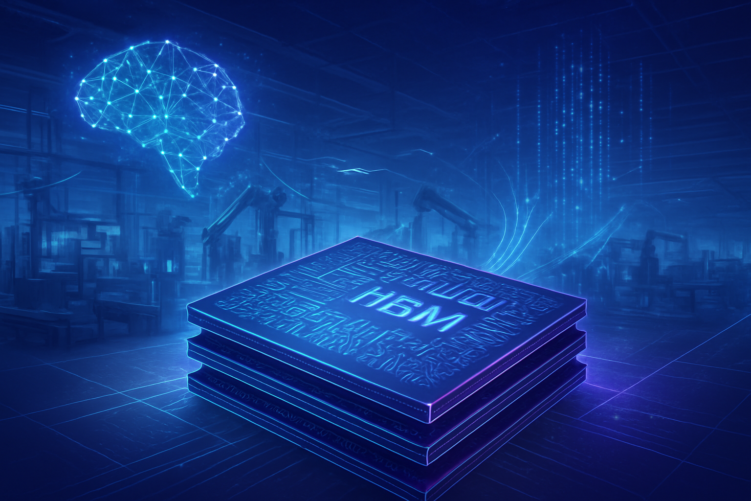
A critical bottleneck and a significant technical challenge emerging from this demand is the unprecedented scarcity of High-Bandwidth Memory (HBM). HBM, a type of stacked synchronous dynamic random-access memory (SDRAM), offers significantly higher bandwidth compared to traditional DRAM, making it indispensable for AI accelerators. HBM revenue is projected to surge by up to 70% in 2025, reaching an impressive $21 billion. This intense demand has triggered a "supercycle" in DRAM, with reports of prices tripling year-over-year by late 2025 and inventories shrinking dramatically. The technical complexity of HBM manufacturing, involving advanced packaging techniques like 3D stacking, limits its production capacity and makes it difficult to quickly ramp up supply, exacerbating the shortage. This contrasts sharply with previous memory cycles driven by PC or mobile demand, where conventional DRAM could be scaled more readily.
Initial reactions from the AI research community and industry experts highlight both excitement and apprehension. While the availability of more powerful hardware fuels rapid advancements in AI capabilities, concerns are mounting over the escalating costs and potential for an "AI divide," where only well-funded entities can afford the necessary infrastructure. Furthermore, the reliance on a few key manufacturers for advanced chips and HBM creates significant supply chain vulnerabilities, raising questions about future innovation stability and accessibility for smaller players.
Corporate Fortunes and Competitive Realignment in the AI Era
The AI-driven semiconductor boom is profoundly reshaping corporate fortunes, creating clear beneficiaries while simultaneously intensifying competitive pressures and strategic realignments across the tech industry. Companies positioned at the nexus of AI hardware and infrastructure are experiencing unprecedented growth and market dominance.
NVIDIA (NASDAQ: NVDA) unequivocally stands as the primary beneficiary, having established an early and commanding lead in the AI GPU market. Its CUDA platform and ecosystem have become the de facto standard for AI development, granting it a significant competitive moat. The company's exceptional revenue growth, particularly from its data center division, underscores its pivotal role in powering the global AI infrastructure build-out. Close behind, Advanced Micro Devices (NASDAQ: AMD) is rapidly gaining traction with its MI series of AI accelerators, presenting a formidable challenge to NVIDIA's dominance and offering an alternative for hyperscalers and enterprises seeking diversified supply. Intel (NASDAQ: INTC), while facing a steeper climb, is also aggressively investing in its Gaudi accelerators and foundry services, aiming to reclaim a significant share of the AI chip market.
Beyond the chip designers, semiconductor foundries like Taiwan Semiconductor Manufacturing Company (TSMC) (NYSE: TSM) are critical beneficiaries. As the world's largest contract chip manufacturer, TSMC's advanced process nodes (5nm, 3nm, 2nm) are essential for producing the cutting-edge AI chips from NVIDIA, AMD, and custom ASIC developers. The demand for these advanced nodes ensures TSMC's order books remain full, driving significant capital expenditures and technological leadership. Similarly, memory manufacturers like Samsung Electronics (KRX: 005930), SK Hynix (KRX: 000660), and Micron Technology (NASDAQ: MU) are seeing a massive surge in demand and pricing power for their HBM products, which are crucial components for AI accelerators.
The competitive implications for major AI labs and tech companies are substantial. Hyperscale cloud providers like Amazon Web Services, Microsoft Azure, and Google Cloud are engaged in a fierce "AI infrastructure race," heavily investing in AI chips and data centers. Their strategic move towards developing custom AI ASICs, often in collaboration with companies like Broadcom (NASDAQ: AVGO), aims to optimize performance, reduce costs, and lessen reliance on a single vendor. This trend could disrupt the traditional chip vendor-customer relationship, giving tech giants more control over their AI hardware destiny. For startups and smaller AI labs, the soaring costs of AI hardware and HBM could become a significant barrier to entry, potentially consolidating AI development power among the few with deep pockets. The market positioning of companies like Synopsys (NASDAQ: SNPS) and Cadence Design Systems (NASDAQ: CDNS), which provide AI-driven Electronic Design Automation (EDA) tools, also benefits as chip designers leverage AI to accelerate complex chip development cycles.
Broader Implications: Reshaping the Global Tech Landscape
The AI-driven semiconductor boom extends its influence far beyond corporate balance sheets, casting a wide net across the broader AI landscape and global technological trends. This phenomenon is not merely an economic uptick; it represents a fundamental re-prioritization of resources and strategic thinking within the tech industry and national governments alike.
This current surge fits perfectly into the broader trend of AI becoming the central nervous system of modern technology. From cloud computing to edge devices, AI integration is driving the need for specialized, powerful, and energy-efficient silicon. The "race to build comprehensive large-scale models" is the immediate catalyst, but the long-term vision includes the proliferation of "Agentic AI" across enterprise and consumer applications and "Physical AI" for autonomous robots and vehicles, all of which will further intensify semiconductor demand. This contrasts with previous tech milestones, such as the PC boom or the internet era, where hardware demand was more distributed across various components. Today, the singular focus on high-performance AI chips and HBM creates a more concentrated and intense demand profile.
The impacts are multi-faceted. On one hand, the advancements in AI hardware are accelerating the development of increasingly sophisticated AI models, leading to breakthroughs in areas like drug discovery, material science, and personalized medicine. On the other hand, significant concerns are emerging. The most pressing is the exacerbation of supply chain constraints, particularly for HBM and advanced packaging. This scarcity is not just a commercial inconvenience; it's a strategic vulnerability. Geopolitical tensions, tariffs, and trade policies have, for the first time, become the top concern for semiconductor leaders, surpassing economic downturns. Nations worldwide, spurred by initiatives like the US CHIPS and Science Act and China's "Made in China 2025," are now engaged in a fierce competition to onshore semiconductor manufacturing, driven by a strategic imperative for self-sufficiency and supply chain resilience.
Another significant concern is the environmental footprint of this growth. The energy demands of manufacturing advanced chips and powering vast AI data centers are substantial, raising questions about sustainability and the industry's carbon emissions. Furthermore, the reallocation of wafer capacity from commodity DRAM to HBM is leading to a shortage of conventional DRAM, impacting consumer markets with reports of DRAM prices tripling, stock rationing, and projected price hikes of 15-20% for PCs in early 2026. This creates a ripple effect, where the AI boom inadvertently makes everyday electronics more expensive and less accessible.
The Horizon: Anticipating Future Developments and Challenges
Looking ahead, the AI-driven semiconductor landscape is poised for continuous, rapid evolution, marked by both innovative solutions and persistent challenges. Experts predict a future where the current bottlenecks will drive significant investment into new technologies and manufacturing paradigms.
In the near term, we can expect continued aggressive investment in High-Bandwidth Memory (HBM) production capacity by major memory manufacturers. This will include expanding existing fabs and potentially developing new manufacturing techniques to alleviate the current shortages. There will also be a strong push towards more efficient chip architectures, including further specialization of AI ASICs and the integration of Neuromorphic Processing Units (NPUs) into a wider range of devices, from edge servers to AI-enabled PCs and mobile devices. These NPUs are designed to mimic the human brain's neural structure, offering superior energy efficiency for inference tasks. Advanced packaging technologies, such as chiplets and 3D stacking beyond HBM, will become even more critical for integrating diverse functionalities and overcoming the physical limits of Moore's Law.
Longer term, the industry is expected to double down on materials science research to find alternatives to current silicon-based semiconductors, potentially exploring optical computing or quantum computing for specific AI workloads. The development of "Agentic AI" and "Physical AI" (for autonomous robots and vehicles) will drive demand for even more sophisticated and robust edge AI processing capabilities, necessitating highly integrated and power-efficient System-on-Chips (SoCs). Challenges that need to be addressed include the ever-increasing power consumption of AI models, the need for more sustainable manufacturing practices, and the development of a global talent pool capable of innovating at this accelerated pace.
Experts predict that the drive for domestic semiconductor manufacturing will intensify, leading to a more geographically diversified, albeit potentially more expensive, supply chain. We can also expect a greater emphasis on open-source hardware and software initiatives to democratize access to AI infrastructure and foster broader innovation, mitigating the risk of an "AI oligarchy." The interplay between AI and cybersecurity will also become crucial, as the increasing complexity of AI systems presents new attack vectors that require advanced hardware-level security features.
A New Era of Silicon: Charting AI's Enduring Impact
The current AI-driven semiconductor boom represents a pivotal moment in technological history, akin to the dawn of the internet or the mobile revolution. The key takeaway is clear: AI's insatiable demand for processing power and high-speed memory is not a fleeting trend but a fundamental force reshaping the global tech industry. Semiconductor sales are not just reaching record highs; they are indicative of a profound, structural shift in how technology is designed, manufactured, and deployed.
This development's significance in AI history cannot be overstated. It underscores that hardware innovation remains as critical as algorithmic breakthroughs for advancing AI capabilities. The ability to build and scale powerful AI models is directly tied to the availability of cutting-edge silicon, particularly specialized accelerators and high-bandwidth memory. The current memory shortages and supply chain constraints highlight the inherent fragility of a highly concentrated and globally interdependent industry, forcing a re-evaluation of national and corporate strategies.
The long-term impact will likely include a more decentralized and resilient semiconductor manufacturing ecosystem, albeit potentially at a higher cost. We will also see continued innovation in chip architecture, materials, and packaging, pushing the boundaries of what AI can achieve. The implications for society are vast, from accelerating scientific discovery to raising concerns about economic disparities and geopolitical stability.
In the coming weeks and months, watch for announcements regarding new HBM production capacities, further investments in domestic semiconductor fabs, and the unveiling of next-generation AI accelerators. The competitive dynamics between NVIDIA, AMD, Intel, and the hyperscalers will continue to be a focal point, as will the evolving strategies of governments worldwide to secure their technological futures. The silicon gold rush is far from over; indeed, it is only just beginning to reveal its full, transformative power.
This content is intended for informational purposes only and represents analysis of current AI developments.
TokenRing AI delivers enterprise-grade solutions for multi-agent AI workflow orchestration, AI-powered development tools, and seamless remote collaboration platforms.
For more information, visit https://www.tokenring.ai/.